前瞻非揮發性記憶體元件之研究
148
0
0
全文
(2) 前瞻非揮發性記憶體元件之研究 Study on Advanced Nonvolatile Memory Devices 研 究 生: 顏 碩 廷. Student: Shuo-Ting Yan. 指導教授: 施 敏 博士 張鼎張 博士. Advisor: Dr. Simon M. Sze Dr. Ting-Chang Chang. 國 立 交 通 大 學 電子工程學系 電子研究所 博 士 論 文 A Dissertation Submitted to the Institute of Electronics College of Electrical Engineering and Computer Science National Chiao Tung University in Partial Fulfillment of the Requirements for the Degree of Doctor of Philosophy in Electronics Engineering June 2004 Hsinchu, Taiwan, Republic of China. 中 華 民 國. 九 十 三. 年. 六 月.
(3) 推. 薦 函. 事由: 推薦電子研究所博士班研究生顏碩廷提出論文,參加國立交 通大學博士論文口試。 說明: 本校電子研究所博士班研究生顏碩廷,業已修畢部訂所需課 程學分,通過博士資格考之學科考試,並完成博士論文「前 瞻非揮發性記憶體元件之研究」初稿,且有數篇相關之論文 發表或送審,茲列舉如下:. International Regular Journals: 1. T. C. Chang, S. T. Yan, P. T. Liu, Z. W. Lin, H. Aoki, and S. M. Sze, Thin Solid Films, Vol. 447-448, January 30, pp. 516-523 (2004). 2. T. C. Chang, S. T. Yan, P. T. Liu, C. W. Chen, H. H. Wu, and S. M. Sze, “Quasi-Superlattice Storage (QS2): A Novel Concept of Multilevel Charge Storage”, accepted by Journal of The Electrochemical Society (2004).. International Letter Journals: 1. T. C. Chang, S. T. Yan, P. T. Liu, C. W. Chen, S. H. Lin, S. M. Sze, “A novel approach for fabricating germanium nanocrystals for nonvolatile memory application”, Electrochem. and Solid-State Lett., 7, G17, (2004). 2. T. C. Chang, S. T. Yan, P. T. Liu, C. W. Chen, S. H. Lin, S. M. Sze, “Study on SONOS nonvolatile memory technology using high-density plasma CVD silicon nitride”, Electrochem. and Solid-State Lett., 7, G112 (2004). 3. T. C. Chang, S. T. Yan, F. M. Yang, P. T. Liu and S. M. Sze, “Memory effect of oxide/SiC:O/oxide sandwiched structures”, Appl. Phys. Lett., 84, 2094 (2004). 4. T. C. Chang, S. T. Yan, P. T. Liu, C. W. Chen, S. H. Lin, S. M. Sze, “A new method of fabricating superior oxide/nitride/oxide gate stack”, has been accepted by Electrochemical and Solid-State Letters (2004). 5. T. C. Chang, S. T. Yan, C. H. Hsu, M. T. Tang, J. F. Lee, Y. H. Tai, P. T. Liu and S. M. Sze, “A distributed charge storage with GeO2 nanodots”, Appl. Phys. Lett., 84, 2581 (2004). 6. T. C. Chang, S. T. Yan, P. T. Liu, C. W. Chen, H. H. Wu, and S. M. Sze, “Leakage behavior of the quasi-superlattice stack for multilevel charge storage”, accepted by Applied Physics Letters..
(4) 7. T. C. Chang, S. T. Yan, Y. T. Chen, P. T. Liu, S. M. Sze, “A Novel Distributed Charge Storage Element Fabricated by the Oxidation of Amorphous Silicon Carbide”, accepted by Electrochemical and Solid-State Letters (2004).. 綜上所陳,顏君已具備國立交通大學電子研究所應有之教育及訓練水 準,謹此推薦顏君參加交通大學電子研究所博士論文口試。. 此致 國立交通大學電子研究所. 電子研究所教授. 施 敏 博士 張鼎張 博士. 中 華 民 國 九 十 三 年 5. 月. 6 日.
(5) 前瞻非揮發性記憶體元件之研究. 研 究 生: 顏 碩 廷. 指導教授: 施. 敏 博士. 張 鼎 張 博士. 國 立 交 通 大 學. 電子工程學系 電子研究所. 摘要. 首先,在 SONOS 非揮發性記憶體的研究方面,本論文利用高密度電漿化學 氣相沈積製作含有多能阱(trap)之載子儲存氮化矽層或其他介電質。由於高密度 電漿化學氣相沈積薄膜,於沈積過程中具有較高的離子轟擊效應,導致形成的薄 膜較緻密且斷鍵陷阱(trap)較多,對電子的捕獲效應較佳,期望達到較大的記憶 窗,以改善記憶體元件的保存時間。高密度電漿氮化矽薄膜比傳統低壓化學氣相 沉積氮化矽,具有較大的記憶窗口。由複立葉轉換紅外線光譜圖可以發現,高密 度電漿氮化矽薄膜由於含有許多 N-H 鍵結作為載子捕獲的陷阱,證明其記憶窗 口較大的原因。在電流-電壓特性方面,雖然高密度電漿能阱比傳統低壓化學氣 相沉積氮化矽多,但漏電特性比較起來,僅大不到一個因次,另外儲存載子在高 溫 150 度下的保存時間亦說明了高密度電漿氮化矽 SONOS 記憶體元件的可靠 性。 此外,我們更針對傳統 ONO 結構的製程方式加以改善,例如在穿隧氧化層 i.
(6) 上方沉積高密度電漿氮化矽薄膜,並加以高溫熱氧化,異於傳統利用低壓化學氣 相沉積作為控制氧化層的直接沉積方式,使閘極堆疊介電層結構漏電極降低及崩 潰電場提高,並獲得期望中具有較佳的介電特性及可靠性。 在載子儲存的介電層方面,除了 Si3N4 之外,以往的研究著重於 Al2O3,TiO2, Ta2O5 等,本論文更進一步地在其它的介電材料中探索,預期找到一種適合的載 子儲存單元絕緣層,例如含氧碳化矽(SiC:O)薄膜,並最佳化之。利用高密度電 漿薄膜直接沉積的方式,製作二氧化矽/SiC:O/二氧化矽的三明治結構。藉由含氧 碳化矽對於不同氧含量的電容-電壓特性圖及電流-電壓特性圖發現,當氧含量依 序漸增時,含氧碳化矽之記憶窗口大小隨氧含量的增加而變小,另外藉由氧含量 的控制,可達到較大的崩潰電壓值。我們亦提出了一個物理模型,解釋含氧量較 少時,崩潰電壓較大的原因。本研究欲針對材料,製程及量測分析方面加以最佳 化之。 關於含氧碳化矽作為載子儲存單元的記憶體元件方面,不同於上述利用高密 度電漿化學氣相沉積的方式製作,我們亦提出了利用在穿隧氧化層上之碳化矽薄 膜熱氧化的方式,使碳化矽薄膜氧化為含氧碳化矽薄膜,作為載子儲存的單元, 最後覆蓋二氧化矽薄膜作為控制氧化層。在碳化矽薄膜的氧化研究方面,我們發 現低溫(800 度)熱氧化比高溫(925 度)熱氧化的含氧碳化矽,具有更高的記憶窗 口,亦即具有較高的載子儲存能力。利用複利葉轉換紅外線光譜儀(FTIR)等材料 分析工具,我們提出了解釋具有較高記憶窗口含氧碳化矽行為的物理模型。 傳統的浮停閘快閃記憶體是利用連續的多晶矽半導體薄膜作為載子儲存的 單元;SONOS 非揮發性記憶體係利用絕緣體氮化矽薄膜,作為載子儲存的單元。 本論文提出了一種利用似超晶格(quasi-superlattice)結構,作為載子儲存的單元。 在 2-3 奈米的穿隧氧化層上方,依序沉積氮化矽,非晶矽,氮化矽,非晶矽,各 約 1-2 奈米,形成似超晶格結構,最後覆蓋氧化矽作為控制氧化層,形成非揮發 性記憶體元件結構。在記憶體特性的表現上,記憶窗口有隨著寫入電壓增大而增 大的趨勢,並且具有明顯的兩個起始電壓偏移抖增的現象。藉由適當的閘極電壓 寫入,此元件具有每個記憶單元(memory cell)兩個位元(bit)的操作能力,只單純 ii.
(7) 由閘極利用 F-N 穿隧寫入,而不是像 SONOS 元件需利用源極與汲極雙向的寫入 與讀取來定義每個記憶單元的兩個位元。本論文針對此似超晶格記憶體元件,提 出了一個物理模型來解釋兩個位元的儲存,並且針對閘極堆疊結構室溫及低溫的 漏電效應,做了物理性的探討。 在奈米晶體非揮發性記憶體之研究方面,首先,我們成功地利用矽化鍺薄膜 熱氧化研製出包覆在氧化矽中的鍺奈米點。在穿隧氧化層上方沉積矽化鍺薄膜, 爾後利用高溫乾氧化,使鍺向下析出於穿隧氧化層上方,矽氧化成二氧化矽作為 控制氧化層(control oxide),形成鍺奈米點包覆於二氧化矽中的結構。由穿透式電 子顯微鏡可知鍺奈米點直徑大為 5.5 奈米,元件的記憶體特性以及可靠性也相當 穩健。當上述鍺奈米點再加以過度熱氧化之後,鍺便會氧化為氧化鍺,形成氧化 鍺奈米點。經由電性量測後發現,氧化鍺奈米點也確實有記憶體特性,另外經由 x-ray absorption near edge spectroscopy (XANES)也證實穿透式電子顯微鏡照片中 的奈米點成分為氧化鍺,我們並且提出了一個物理模型來解釋此元件之記憶體效 應。 除了半導體奈米點之外,本論文亦針對金屬奈米點做深入的研究。在金屬奈 米點的製作方面,首先在穿隧氧化層上方沉積矽化鎢薄膜,並覆蓋上一層非晶矽 薄膜約 8 奈米。當試片經過高溫熱氧化之後,成分矽會氧化為二氧化矽作為控制 氧化層,而矽化鎢中的金屬成分鎢會傾向向下析出,成核於穿隧氧化層上方,形 成鎢奈米點,作為載子儲存的單元。在氧化的過程中,氧化參數需嚴格控制,否 則金屬矽化鎢可能會氧化不足仍為薄膜,或是氧化過度將金屬鎢全部氧化。關於 金屬鎢奈米點記憶體元件的記憶體特性,其具有相當大的記憶窗口(memory window)可作為定義 0 或 1 的依據,另外,此元件反覆操作的忍耐度(endurance) 也可以達到一百萬次以上。. iii.
(8) Study on Advanced Nonvolatile Memory Devices. Student: Shuo-Ting Yan. Advisor: Dr. Simon M. Sze. Dr. Ting-Chang Chang. Department of Electronic Engineering and Institute of Electronics College of Electrical Engineering and Computer Science National Chiao Tung University. Abstract. We have studied experimentally and theoretically three types of nonvolatile semiconductor. memories:. quasi-superlattice. the. memory. SONOS, devices.. the On. nanocrystal/nanodot, the. study. and of. the the. silicon-oxide-nitride-oxide-silicon (SONOS) nonvolatile memory technology, high density plasma chemical vapor deposition (HDPCVD) is used to fabricate trap-rich silicon nitride or other dielectrics as the charge storage element. It is observed that the densified and trap-rich silicon nitride film from HDPCVD possesses a larger memory window than that of the conventional low pressure chemical vapor deposited (LPCVD) silicon nitride. It is found from the Fourier Transform Infrared Spectrum (FTIR) that there are N-H bonds within the HDPCVD silicon nitride as the charge trapping sites, which certifies the reason of the larger memory window. The HDPCVD silicon nitride is deposited on the tunnel oxide, followed by a high temperature oxidation process. As iv.
(9) compared to the LPCVD deposition as the control oxide, the HDPCVD processes result in a lower leakage current and higher breakdown voltage. In addition to silicon nitride as the storage layer, we have also studied the oxide/SiC:O/oxide sandwiched structures using HDPCVD processes. From the capacitance-voltage and current-voltage characteristics of oxygen-incorporated silicon carbide with different oxygen content, it is observed that the memory window is decreased with increasing the oxygen content. By controlling the oxygen content, a higher breakdown voltage can be achieved. A physical model is proposed to explain the higher breakdown voltage with less oxygen content of the oxygen-incorporated silicon carbide. We have also studied the thermal oxidation of SiC layer on the tunnel oxide as the charge storage layer followed by control oxide capped. In the study of the oxidation of SiC, it is found that low temperature (800 ℃) oxidized SiC shows a larger memory window than that of the high temperature (925 ℃) oxidized SiC. Using the FTIR spectroscopy, a physical model is proposed to explain the behavior of low temperature oxidized SiC with larger memory window. On the study of the quasi-superlattice structure, we have sequentially deposited 1-2 nm silicon nitride and a-Si on a 2-3 nm tunnel oxide in two cycles to form the quasi-superlattice structure. Finally, SiO2 is capped as the control oxide. The memory window is increased with the programming voltage. Also, two sudden rises of the threshold voltage shift are observed. By suitably operated gate voltage, this memory device shows the capability of the operation of 2-bit per cell. The 2 bits can be operated and defined by F-N tunneling rather than the source/drain bidirectional programming and reading of the conventional SONOS memory devices. A physical model is proposed to explain the 2-bit storage and the investigation of room and low temperature leakage behavior of the gate stack is also considered. On the study of nanocrystal nonvolatile memory devices, we have successfully fabricated germanium nanocrystals embedded in silicon dioxide by the thermal oxidation of SiGe. SiGe layer is deposited on the tunnel oxide, followed by high v.
(10) temperature thermal oxidation. The Ge element of the SiGe layer is downward segregated and precipitated on the tunnel oxide and the Si element is oxidized into silicon dioxide as the control oxide. From the analyses of the TEM micrograph, it is observed that the size of the Ge nanocrystals is around 5.5 nm. The memory effects and the reliability of the memory are characterized robust. As the germanium nanodots are over-oxidized, the germanium nanodots are oxidized into germanium oxide dots. It is found that the germanium oxide exhibits an apparent memory effects. Also, the x-ray absorption near edge spectroscopy (XANES) analysis certifies the composition of the GeO2 nanodots in the TEM micrograph. A physical model is proposed to demonstrate the memory effects of the GeO2 memory device. In addition to semiconductor nanocrystals, metal nanodots are investigated. On the aspect of the fabrication of metal nanodots, tungsten nanodots are firstly demonstrated. The tungsten silicide layer is physically deposited on the tunnel oxide and an amorphous Si layer is capped on the silicide layer. As the sample is high temperature thermally oxidized, the silicon element is oxidized into silicon dioxide as the control oxide and the tungsten element tends to segregate downward and precipitate on the tunnel oxide. During the oxidation process, the parameters of the oxidation need to be well control or the tungsten silicide will be under-oxidized or over-oxidized. The tungsten nanocrystal memory device shows a large memory window to be defined as “1” or “0”. Also, the endurance characteristics of the memory device achieve 106 write/erase cycles which show the robustness of the memory device.. vi.
(11) 誌謝 執筆至此,表示論文寫作已告一段落,在寫作的過程中,一直在思索該如 何寫致謝這一部分,偏偏到了現在開始動筆了,卻不知道如何用文字表達我的 感謝之意。我一直覺得生命中充滿貴人,來到交大之後,師承的兩位師長也就 是我的貴人。施敏教授給學生很自由的發揮空間,言談之中處處充滿啟發,讓 我在做研究時,找到方向,更常藉著一些小故事,鼓勵我應該更努力;在待人 處世上,施教授的風格業已成為學生心目中的人生導師。張鼎張教授對於我的 研究方面的指導更是不遺餘力,不僅積極激發學生的創意,對於學生研究上的 困難,張教授也非常用心協助學生解決問題。此外,張教授亦會親切的融入學 生的生活,關心學生,與學生一同歡樂。在兩位老師的師門之下,那種充滿歡 笑聲的環境與氣氛,是會令我終身難忘的。所謂「一日為師,終身為父」 ,對兩 位老師的感激之情,竟像八月的桂花香一般,濃郁芬芳,久久無法散去。 此外,我非常感謝國家奈米元件實驗室劉柏村博士,劉博士是一位令我十 分尊敬的學長,在研究上不僅提供了許多資源給我,更幫助我在論文寫作上更 加順利,不勝感激。同時,也要感謝國家奈米元件實驗室林詩融小姐,在實驗 及行政上給予充分的幫忙與協助,希望林小姐可以像 Iris 女神一樣,人如其名。 我感覺到非常地榮幸,在我的論文口試當天,有許多的口試委員親自蒞臨 指導:陳力俊教授、雷添福教授、陳明哲教授、曾俊元教授、羅正忠教授、胡 正明教授、盧火鐵博士以及劉柏村博士。因為你們的指導以及鼓勵,才使得我 的博士論文更加充實,由衷感謝你們。 值得一提的是我的好夥伴們,沒有你們的鼓勵與分享,沒有我的今天。小 鳴,實實在在的好學長;紀文,實驗室的開心果,大哥的典範;仁宏,實驗上 的最佳合作拍檔;炳宏,認真的同袍;峻豪、大山、世青、敏全、富明、興華、 泩宏、世仰、炳麟、元均、子軒、育廷、稚軒、泓緯,活潑又有衝勁的學弟們; 柏儀,和我一起想題目想實驗的陽光同學;宏年,忍受我的作息和搖滾樂的好. vii.
(12) 室友;建豪,天才同學,會邀我一起到劇場的同伴;獻德,我的另一位貴人, 沒有你沒有我的今天;家齊,志同道合的老同學,未來事業夥伴;凰君,難得 的知音,會記得從國外買 DVD 送我的好朋友;漢譽,另一個天才,登山旅遊的 好夥伴;雅雯、明哲、阿標;隆傑、雄、岳鋒;小野猪、思宏、雅玲;太多太 多要感謝的人,可能漏掉了,但不會忘記的。你們支持我陪伴我,給我力量完 成學業,這份感激是無法抹滅的。 不會忘記的是,我親愛的家人們,老爸老媽老弟老妹,我最忠實的聽眾們, 我最有力量的後盾,我最堅固的避風港,感謝你們。 2004 年 盛夏 碩廷. viii.
(13) Contents. Chinese Abstract. ------------------------------------------------------------- i. English Abstract. ------------------------------------------------------------- iii. Acknowledgment ----------------------------------------------------------- vi Contents ----------------------------------------------------------------------viii Table Captions. --------------------------------------------------------------- x. Figure Captions --------------------------------------------------------------xi Chapter 1 Introduction 1.1 General Background. --------------------------------------------------- 1. 1.2 Organization of the Thesis --------------------------------------------11. Chapter 2. Study on SONOS Nonvolatile Memory Technology Using High-Density Plasma Chemical Vapor Deposited Silicon Nitride 2.1 Motivation ------------------------------------------------------------- 19 2.2 Experimental Procedures --------------------------------------------- 20 2.3 Results and Discussions ---------------------------------------------- 21 2.4 Conclusion. --------------------------------------------------------------23. A New Method of Fabricating Superior Oxide/Nitride/Oxide Gate Stack---------------------------------------------------------------------------- 23. Chapter 3. Memory Effect of Oxide/Oxygen-Incorporated Silicon Carbide/Oxide Sandwiched Structure 3.1 Motivation ------------------------------------------------------------- 36 3.2 Experimental Procedures --------------------------------------------- 37 3.3 Results and Discussions ---------------------------------------------- 38 3.4 Conclusion --------------------------------------------------------------- 40 A Novel Distributed Charge Storage Element Fabricated by the Oxidation of Amorphous Silicon Carbide--------------------------------- 40. ix.
(14) Chapter 4 A Novel Approach of Fabricating Germanium. Nanocrystals for Nonvolatile Memory Application 4.1 Motivation ------------------------------------------------------------- 58 4.2 Experimental Procedures --------------------------------------------- 59 4.3 Results and Discussions ---------------------------------------------- 60 4.4 Conclusion---------------------------------------------------------------- 63 A distributed charge storage with GeO2 nanodots------------------------63 Supplement---------------------------------------------------------------------67. Chapter 5 Electron charging and discharging effects of. tungsten nanocrystals embedded in silicon dioxide for low-power nonvolatile memory technology 5.1 Motivation. ----------------------------------------------------------- 80. 5.2 Experimental Procedures -------------------------------------------- 81 5.3 Results and Discussions. --------------------------------------------- 82. 5.4 Conclusion -------------------------------------------------------------- 84. Storage (QS2): Concept of Multilevel Charge Storage. Chapter 6 Quasi-Superlattice. A. Novel. 6.1 Motivation ------------------------------------------------------------- 89 6.2 Experimental Procedures -------------------------------------------- 90 6.3 Results and Discussions. -------------------------------------------- 90. 6.4 Conclusion -------------------------------------------------------------- 96. Chapter 7 Conclusions and Suggestions for Future Work 7.1 Conclusions. -----------------------------------------------------------105. 7.2 Suggestions for future work ----------------------------------------110. References -------------------------------------------------------------------------------111 Vita. -----------------------------------------------------------------------------------------126. Publication List ------------------------------------------------------------------------127. x.
(15) Table Captions Chapter 3 Table 3-1. The parameters of the deposition of the SiC:O films.. xi.
(16) Figure Captions Chapter 1 Fig. 1-1. The structure of the conventional floating gate nonvolatile memory device. Continuous poly-Si floating gate is used as the charge storage element and ONO sandwiched structure is used as the control oxide.. Fig. 1-2. The structure of the SONOS nonvolatile memory device. The nitride layer is used as the charge-trapping element.. Fig. 1-3. The structure of the nanocrystal nonvolatile memory device. The semiconductor or metal nano-dots are used as the charge storage element instead of the continuous poly-Si floating gate.. Fig. 1-4. The development of the gate stack of SONOS EEPROM memory devices. The optimization of nitride and oxide films has been the main focus in recent years.. Fig. 1-5. The energy band diagrams of the write/erase operation for a SONOS device.. Fig. 1-6. Schematic illustration of the device structure. Indicated structure dimensions are obtained by transmission electron microscopy and spectroscopic ellipsometry measurement. 18 nm layer of SiO2 was deposited at 470 °C by low pressure chemical vapor deposition.. Chapter 2 Fig. 2-1. (a) The band diagrams of the write/erase operation of the MONOS structure with different gate polarities. The inset is the ONO gate-stacked structure in this study. (b) The C-V hysteresis of the capacitor is performed by sweeping from 12 V ~ (-12) V and in reverse.. Fig. 2-2. Fourier transform infrared spectroscopy (FTIR) of the HDPCVD and LPCVD nitrides.. xii.
(17) Fig. 2-3. The leakage current of LPCVD and HDPCVD silicon nitride ONO gate stack. The leakage current of the HDPCVD SiNx ONO structure is slightly higher than that of the conventional LPCVD Si3N4 within an order.. Fig. 2-4. The threshold-voltage shift versus different periods of time when the samples are heated at 150 ℃.. Fig. 2-5. FTIR spectrum of the surface oxide layer and HDP nitride layer stack with the background spectrum of Si wafer and tunnel oxide deposited.. Fig. 2-6. The C-V hysteresis after forward (from inversion to accumulation region) and reverse voltage sweeping (from accumulation to inversion region).. Fig. 2-7. The current-voltage characteristics of the ONO gate stack.. Fig. 2-8. The endurance characteristics of the memory device retains an obvious memory window of 0.91 V after 106 5/(-5) V write/erase cycles. The inset exhibits the C-V hysteresis after 106 write/erase cycles.. Chapter 3. Fig. 3-1. The structure of the MOIOS device shown in this work.. Fig. 3-2. The C-V hysteresis for different samples under 7 and (-7) V bidirectional voltage sweeping.. Fig. 3-3. The band diagrams of the “write” and “erase” operation.. Fig. 3-4. FTIR spectrum of the deposited SiC:O film.. Fig. 3-5. (a) The FTIR absorbance of Si-C bonds and (b) FTIR absorbance of Si-H bonds.. Fig. 3-6. The structural formula of the proposed model. As the oxygen content is increased, both Si-C and Si-H bonds may be decreased, which renders the decrease of the dangling bonds. The dotted lines indicate the dangling xiii.
(18) bonds of the C-H bonds which are not well-bound. Fig. 3-7. The leakage current characteristics of the sandwiched structure. The breakdown voltage is increased with the decrease of oxygen content.. Fig. 3-8. The band diagram shows that when the electrons are captured in a charge-trapping layer with rich charge-trapping sites, the conduction band of the charge-trapping layer will be lifted, which forms an energy barrier for the conductive electrons.. Fig. 3-9. The process flow proposed in this work.. Fig. 3-10 The TEM micrograph of the SiCO stack. The thickness of the oxidized SiCO layer is estimated to be around 22.5 nm. Fig. 3-11 The capacitance-voltage (C-V) hysteresis of the MOIOS structure. The electrical C-V measurements are performed by bidirectional voltage sweeping from 5 V ~ (-7) V and (-7) V ~ 5 V. Fig. 3-12 FTIR spectra of the SiCO stack with different oxidation temperatures (a) Si-O bonds (b) Si-C bonds.. Chapter 4 Fig. 4-1. Ge nanocrystals formed after high temperature rapid thermal annealing in N2 gas. The insert shows the gate stack in this study.. Fig. 4-2. The hysteresis of capacitance-voltage (C-V) measurements after 5V and –5V sweeping.. Fig. 4-3. (a) The leakage current of the gate dielectric with and without Ge nanocrystals (b) The relation of ln(J/E2) versus (1/E) shows the conduction mechanism is F-N tunneling and the insert shows the band diagrams of writing and erasing operation.. Fig. 4-4. The threshold-voltage shift is measured with different periods of time xiv.
(19) when the sample is heated at 150 ℃.. Fig. 4-5. The cross-sectional TEM micrograph of an oxide/GeO2 nano-dots/oxide stacked structure.. Fig. 4-6. The XANES spectra of the investigated sample and standard samples.. Fig. 4-7. The capacitance-voltage hysteresis after the bidirectional bias sweeps between 5 V and (-5) V.. Fig. 4-8. The band diagrams of the operation of the novel distributed charge storage with GeO2 nano-dots.. Fig. 4-9. The process flow of fabricating Ge nanocrystals by rapid oxidation.. Fig. 4-10 The Raman spectrum of the gate stack after the capping of control oxide. It is clearly observed that germanium precipitation is formed after the oxidation process of SiGe layer. Fig. 4-11 The C-V hysteresis of the gate stack after the densification of the control oxide. The pronounced memory effects of the Ge nanocrystals embedded in silicon dioxide are shown with different programming voltages.. Chapter 5 Fig. 5-1. A typical bright-field, cross-section TEM image. The W nanocrystals show a dark contrast on a gray background.. Fig. 5-2. The FTIR spectrum of the gate dielectric exhibits a sharp Si-O bonding type at around 1075 cm-1 and a W-W bonding type at around 714 cm-1, indicating no apparent W-O, W-O-W, or O-W-O bonds.. Fig. 5-3. (a) The capacitance-voltage (C-V) hysteresis after bidirectional sweeps, which implies the electron charging and discharging effects of tungsten nanocrystals embedded in SiO2 and (b) the band diagrams of “write” and “erase” operations with different gate polarities of the memory device. xv.
(20) Fig. 5-4. The endurance characteristics, after different write/erase cycles, of the tungsten nanocrystal memory device. The write and erase voltages are 3 and (-4) V, respectively.. Chapter 6 Fig 6-1. The cross-sectional figure of the quasi-superlattice structure.. Fig 6-2. The ideal energy band diagram of the QS2 memory device at V=0.. Fig 6-3. C-V hysteresis after the bi-directional voltage sweeping. The erasing voltage is fixed at (-7) V.. Fig 6-4. Gate voltage dependence of the memory window. There are two sudden rises of the threshold voltage shift observed, which are taken place at around 5 and 9.5 V.. Fig 6-5. The band diagram of the memory device under programming. Under suitably operated voltage, two apparent states of charge storage can be distinguishable.. Fig 6-6. The current density-voltage (J-V) characteristics for both room temperature and 50 K. The inset shows the local amplification of the J-V curve at 50 K.. Fig 6-7. The ideal energy band diagram of the quasi-superlattice stack under zero bias with split energy levels.. Fig 6-8. (a) The energy band diagram of resonant tunneling at around 2 V between the two a-Si layers (b) the band diagram for 2 V < applied gate voltage <5.2 V.. xvi.
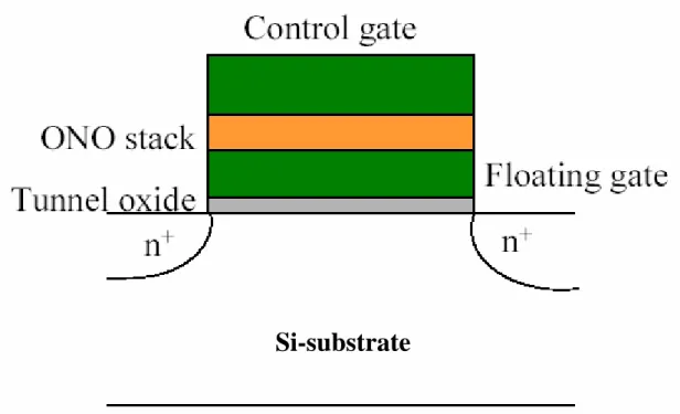
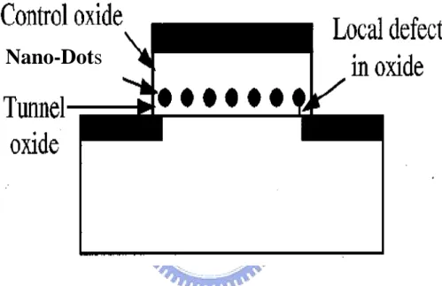
(21) Chapter 1. Introduction. 1.1 General Background. In 1960’s, due to the high cost, large volume, and high power consumption of the magnetic-core memory, the electronic industries urgently needed a new kind of memory device to replace the magnetic-core memory. In 1967, D. Kahng and S. M. Sze invented the floating-gate (FG) nonvolatile semiconductor memory at Bell Labs [1.1]. To date, the stacked-gate FG device structure, as shown in Fig. 1-1, continues to be the most prevailing nonvolatile-memory implementation, and is widely used in both standalone and embedded memories. The invention of FG memory impacts more than the replacement of magnetic-core memory, and creates a huge industry of portable electronic systems. The most widespread memory array organization is the so-called Flash memory, which has a byte-selectable write operation combined with a sector “flash” erase. Although a huge commercial success, conventional FG devices have their limitations. The most prominent one is the limited potential for continued scaling of the device structure. This scaling limitation stems from the extreme requirements put on the tunnel oxide layer. On the one hand, the tunnel oxide has to allow quick and efficient charge transfer to and from the FG. On the other hand, the tunnel oxide needs to provide superior isolation under retention, endurance, and disturbed conditions in order to maintain information integrity over periods of up to a decade. Once the tunnel oxide has been created a leaky path, all the stored charge in the floating gate 1.
(22) will be lost. When the tunnel oxide is thinner for the first consideration, the retention characteristics may be degraded. And when the tunnel oxide is made thicker to take the isolation into account, the speed of the operation will be slower. Therefore, there is a tradeoff between speed and reliability and the thickness of the tunnel oxide is compromised to about 8-11 nm, which is barely reduced over more than five successive generations of the industry [1.2]. To overcome the scaling limits of the conventional FG structure, two candidates are mostly mentioned, SONOS [1.3-1.5] and nanocrystal nonvolatile memory devices [1.6-1.8]. As for SONOS in Fig. 1-2, the nitride layer is used as the charge-trapping element. The intrinsic distributed storage takes an advantage of the SONOS device over the FG device, its improved endurance, since a single defect will not cause the discharge of the memory [1.5]. Tiwari et al. [1.6] for the first time demonstrated the Si nanocrystal floating gate memory device in the early nineties. As shown in Fig. 1-3, the local leaky path will not cause the fatal loss of information for the nanocrystal nonvolatile memory device. Also, the nanocrystal memory device can maintain good retention characteristics when tunnel oxide is thinner and lower the power consumption [1.6-1.8].. 1.1.1 SONOS nonvolatile memory devices. From mobile computer to wireless applications, silicon-oxide-nitride-oxide-silicon (SONOS) nonvolatile semiconductor memories (NVSMs) meet the memory challenges of a small-scale world. In general, NVSMs are required to withstand up to 10-100 K program/erase cycles (endurance) with 10-year memory retention at temperatures as high as 125 ℃. The term “endurance” refers to the ability of the NVSM to withstand repeated program cycles and still meet the specification in the 2.
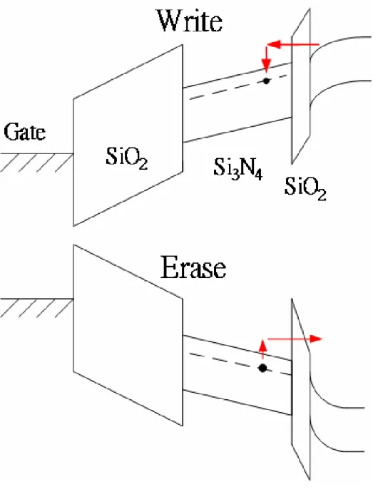
(23) data sheet. The term “retention” describes the ability of the NVSM to store and recover information after a number of program cycles at a specified temperature. In applications where radiation hardness is an important issue, the technology requires radiation-hardened field dielectric processes to minimize the build-up of radiation-induced parasitic leakage. Advancements in ultra-thin tunnel oxides during the 1990s have opened the path to improve performance and reliability for NVSMs based on SONOS technology [1.9]. Figure 1-4 illustrates the progression of device cross section, which has led to the present SONOS device structure. The optimization of nitride and oxide films has been the main focus in recent years. Initial device structures in the early 1970s were p-channel metal-nitride-oxide-silicon (MNOS) structures with aluminum gate electrodes and thick (45 nm) silicon nitride charge storage layers. Write/erase voltages were typically 25-30 V. In the late 1970s and early 1980s, scaling moved to n-channel SNOS devices with write/erase voltages of 14-18 V. In the late 1980s and early 1990s, n- and p-channel SONOS devices emerged with write/erase voltages of 5-12 V. Figure 1-5 illustrates the write/erase operation using an energy-band diagram. The electrons injected from the channel are trapped in the forbidden gap of the silicon nitride film. The electrons, which are not trapped in the nitride film, tunnel through the blocking oxide into the gate electrode. If the poly-Si gate is doped p+, then holes may tunnel from the gate to the silicon nitride valence band, thereby compensating the trapped electrons and reducing the threshold voltage shift. During the erase operation, holes are injected from the substrate into the silicon nitride valence band where they are trapped in a manner similar to electrons. The free holes pile up at the blocking oxide interface because of the larger barrier height (5 eV). Electrons may tunnel from the gate electrode into the nitride compensating the injected holes. A larger barrier for holes (4.7 eV) requires tunnel oxides to be less than 2.5 nm for efficient tunneling and, therefore, “hole tunneling” depends strongly on the 3.
(24) tunnel oxide thickness. Additionally, electrons may tunnel from the valence band of the gate electrode; however, the barrier height for this process is increased by the silicon bandgap (1 eV) as compared with the tunneling from the conduction band. Thus, in summary, for SONOS device operation both carrier types are involved in the transport process. There are a number of applications for SONOS NVSMs, with particular emphasis on “drop-in” modules for the application-specific integrated circuits (ASICs) such as wireless application, embedded NVSM in microcontrollers, and the so-called smart cards. Future smart cars in public transport schemes will be operated using RF data transmission without the need for external contacts and power supplies. SONOS NVSMs may be employed in mobile computing systems such as handheld PCs and notebook and subnotebook PCs; digital still picture cameras; smart digital phones; data acquisition systems for industry, commerce, and military; audio recorders; GPS systems for automobiles, ships, and planes; and communication equipments, including cellular base stations, PBS equipment, and digital routing switches. In addition, there are opportunities for programmable weights in adaptive signal processing and the replacement of DRAMs in dynamic memories since SONOS NVSMs have a small cell size and immunity to single event upset [1.10]. With one-transistor cell (1TC) and the isolation of the stored charge by an insulator, the SONOS device becomes a major challenge to DRAM technology. To improve the device performance of the SONOS technology, the optimization of the ONO stack has been the main considerations currently. She et al. demonstrated jet vapor deposited (JVD) silicon nitride as a tunnel dielectric for flash memory device application. Compared to conventional devices with SiO2 tunnel dielectric, faster programming speed as well as better retention time are achieved with low programming voltage [1.11]. Reisinger et al. [1.12] proposed a SONOS structure with 4.
(25) a p+ doped silicon gate instead of the commonly used n+ gate. In the erase mode, the p+ gate prevents the Fowler Nordheim tunneling of electrons from the conduction band of the gate into the silicon nitride film. Eitan et al. [1.13] proposed a novel localized 2-bit nonvolatile memory cell named as NROMTM. The two-bit operation is performed by charge storage on source- and drain-side silicon nitride layer. Programming is performed by channel hot electron injection and erased by tunneling enhanced hot hole injection. Their read methodology is very sensitive to the location of trapped charge above the source and the single device cell has a two physical bit storage capability. Currently, the 2-bit-per-cell device has become a significant impact for the nonvolatile memory industry. In addition to the horizontal SONOS structure, Lee et al. demonstrated a multilevel vertical channel SONOS nonvolatile memory device on SOI substrate [1.14]. The vertical channel SONOS memory cell is fabricated using 0.12 μm SOI standard logic process for the next generation flash memory cell with ultra high density. With 57 nm wide vertical channel and 1.5 nm tunnel oxide, the vertical channel SONOS shows the scaling breakthrough beyond 0.10 μm flash memory and the multilevel operation with negative programming voltages. The consecutive scaling of the SONOS technology also drives the industry of flash memory approaching the high density, low power consumption, and improved data retention and endurance EEPROM’s [1.15]. Differing from the storage element of silicon nitride of SONOS technology, King et al. proposed another charge storage element such as silicon rich oxide for dynamic or quasi-nonvolatile memory application [1.16]. Using the traps in the silicon rich oxide layer for charge storage, the symmetrical write/erase characteristics were achieved. Also, this memory cell has an erase time much shorter than the values of similar devices reported in the literatures. Low-voltage (5-10 V) SONOS NVSMs may be scaled in cell size to 6F2 (F=feature 5.
(26) size) and perhaps even smaller in the years to come. The simplified ONO gate stack in SONOS memory transistors lends itself to the economics of scaled CMOS circuits. The compatibility of SONOS technology with advanced CMOS logic technology permits economical integration of NVSMs as embedded EEPROMs in ASIC chips. Finally, radiation hardness provides a unique and important feature for advanced military and space systems.. 1.1.2 Nanocrystal nonvolatile memory devices. Storing charges on a single node (the FG node) makes the conventional memory structure particularly prone to failure of the FG isolation. One weak spot in the tunnel oxide is sufficient to create a fatal discharge path, compromising long-term nonvolatility. One way to alleviate the scaling limitation of the conventional FG device, while still preserving the fundamental operating principle of the memory, is to rely on distributed charge storage instead. Nanocrystal nonvolatile memories, first introduced in the early 1990s, are one particular implementation of that concept. In a nanocrystal NVSM device, charge is not stored on a continuous FG poly-Si layer, but instead on a layer of discrete, mutually isolated, crystalline nanocrystals or dots. Each dot will typically store only a handful of electrons; collectively the charges stored in these dots control the channel conductivity of the memory transistor. As compared to conventional stacked gate NVSM devices, nanocrystal charge storage offers several advantages, the main one being the potential to use thinner tunnel oxide without sacrificing nonvolatility. This is a quite attractive proposition since reducing the tunnel oxide thickness is a key to lowering operating voltages and/or increasing operating speeds. This claim of improved scalability results not only from the distributed nature of the charge storage, which makes the storage more 6.
(27) robust and fault-tolerant, but also from the beneficial effects of Coulomb blockade [1.7]. Quantum confinement effects (bandgap widening; energy quantization) can be exploited in sufficiently small nanocrystal geometries (sub-3 nm dot diameter) to further enhance the memory’s performance. There are other important advantages though. First, nanocrystal memories use a more simplified fabrication process as compared to conventional stacked-gate FG NVSM’s by avoiding the fabrication complications and costs of a dual-poly process. Further, due to the absence of drain to FG coupling, nanocrystal memories suffer less from drain induced barrier lowering (DIBL) and therefore have intrinsically better punchthrough characteristics. One way to exploit this advantage is to use a higher drain bias during the read operation, thus improving memory access time. Alternatively, it allows the use of shorter channel lengths and therefore smaller cell area (i.e., lower cost). Finally, nanocrystal memories are characterized by excellent immunity to stress induced leakage current (SILC) and oxide defects due to the distributed nature of the charge storage in the nanocrystal layer. There are, however, some intrinsic weaknesses as well. Of particular importance is the low capacitive coupling between the external control gate and the nanocrystal charge storage layer. This does not only results in higher operating voltages, thus offsetting the benefits of the thinner tunnel oxide, it also removes an important design parameter (the coupling ratio) typically used to optimize the performance and reliability tradeoff. As for the fabrication processes, a first requirement is the aerial density of the nanocrystal dots. A typical target is a density of at least 1012 cm-2. This is equivalent to approximately 100 particles controlling the channel of a memory FET with 100×100 nm2 active area, and requires particle size of 5-6 nm and below. Second, the fabrication process should result in a planar nanocrystal layer, i.e., the thickness of the dielectric layer separating the nanocrystal and the substrate should be well controlled. 7.
(28) Poor control of the tunnel oxide thickness will result in wider threshold voltage distributions and will increase the number erratic bits. More generally, good process control is needed with regards to such nanocrystal features as: size and size distribution, inter-crystal interaction (lateral isolation), uniformity of aerial crystal density, and crystal doping (type and level). Finally, it is preferred that the fabrication process is simple and that it uses standard semiconductor equipments. Several nanocrystal fabrication processes have been demonstrated. Kim et al. [1.17] used conventional LPCVD reactor to fabricate Si nanocrystals at 620 ℃. A high density of about 5×10¹¹/cm2 was obtained on nitride surface, and the density was more than three times larger than that on oxide [1.18-1.19]. Kanjilal et al. demonstrated a sheet of spherical, well-separated, crystalline Ge nanodots embedded in SiO2 on top of p-(001) Si wafer, fabricated by molecular beam epitaxy (MBE) combined with rapid thermal processing and characterized structurally and electrically [1.20]. To fabricate Ge nanocrystals, the oxidation of SiGe contained films has been utilized [1.21]. As the SiGe layer is oxidized, the Ge element will be downward segregated and Si will be oxidized into SiO2 [1.22-1.34]. Ostraat et al. proposed an aerosol silicon nanocrystal nonvolatile memory device with large threshold voltage shift ( >. 3V),. sub-microsecond program times, millisecond erase times, excellent endurance (>105 program/erase cycles), and long term nonvolatility (>106 sec) [1.35]. Differing from the required single planar nanocrystal layer, Ohba et al. proposed a novel Si dot memory whose floating gate consists of self-aligned doubly stacked Si dots. A lower Si dot exists immediately below an upper dot and lies between thin tunnel oxides. It is experimentally shown that charge retention is improved compared to the usual single layer Si dot memory. A theoretical model considering quantum confinement and Coulomb blockade in lower Si dot explains the experimental results consistently, and shows that charge retention is improved exponentially by lower dot size scaling [1.36]. 8.
(29) Qu et al. presented an approach for synthesizing Ge nanocrystals embedded in amorphous silicon nitride films [1.37]. On the basis of preferential chemical bonding formation of Si-N and Ge-Ge, thin films with Ge clusters embedded in amorphous silicon nitride matrix have been prepared by plasma enhanced chemical vapor deposition (PECVD) with reactant gases of SiH4, GeH4, and NH3 mixed in hydrogen plasma at 250 ℃. Park et al. [1.38] also utilized PECVD to form Si nanocrystals embedded in silicon nitride film. They presented the electron charging and discharging effects of the Si nanocrystals embedded in SiNx film. Capacitance-voltage hysteresis is used to inspect the memory effects of the nanocrystal memory devices [1.39]. In addition to semiconductor nanocrystals, Liu et al. described the design principles and fabrication processes of metal nanocrystals [1.40-1.41]. The advantages of metal nanocrystals over their semiconductor counterparts include higher density of states, stronger coupling with the channel, better size scalability, and the design freedom of engineering the work functions to optimize the device characteristics. A self-assembled nanocrystal formation process by rapid thermal annealing of ultra thin metal film deposited on top of tunnel oxide is developed and integrated with NMOSFET devices. Due to the minimization of the surface energy of the metal film under rapid thermal annealing, the driving force results in a discrete layer of metal nanocrystals reside on tunnel oxide. As for the tunnel dielectric for the nanocrystal nonvolatile memory devices, Baik et al., as shown in Fig. 1-6, proposed a tunnel barrier structure that is composed of silicon dioxide and amorphous carbon (a-C) to attain enhanced charge retention without degradation in the injection efficiency [1.42]. The deposition of ultra thin carbon layer as well as nanocrystal array was performed using photochemical vapor deposition (photo-CVD), because photo-CVD is known to have fine thickness controllability in nanometer scale [1.43-1.44]. The first tunnel barrier of SiO2 is formed by oxidation at 400 ℃ under ultraviolet light irradiation 9.
(30) [1.45]. Additionally, high-k tunnel dielectrics were investigated for Si nanocrystal memory devices [1.46-1.48]. Results show that due to its unique band asymmetry in programming and retention mode, the use of high-k dielectric on Si channel offers lower electron barrier height at dielectric/Si interface and larger physical thickness, results in a much higher Jg,programming/Jg,retention ratio than that in SiO2 and therefore faster programming and longer retention. The programming is considered as the electron injection from the channel under positive bias operation for an NMOSFET memory device. However, the programming and erasing mechanisms of p-channel nanocrystal memory devices were also investigated by Han et al. [1.49]. The comparison of retention between programmed holes and electrons shows that holes have longer retention time. As the size and size distribution of the nanocrystals have been considered, She et al. [1.50] made a conclusion on Ge nanocrystal memory device that nanocrystal size around 5 nm is preferred to achieve fast programming speed and longer retention time, and the size should not be scaled below that. The quantum confinement effect for Ge nanocrystals smaller than 5 nm is very significant so that the retention time is shorter and the programming time is longer. Nanocrystal memories have been presented in the mid-nineties as a possible alternative to conventional FG NVSMs devices, by allowing a further decrease in the tunnel oxide thickness. In particular, nanocrystal memories promise to enable a further scaling of the tunnel oxide, by relying on Coulomb blockade effects in small semiconductor geometries and on the enhanced robustness and fault-tolerance of distributed charge storage. Research in this area has focused on the development of nanocrystal materials and fabrication processes, and on the integration of nanocrystal-based storage layers in actual memory devices. Promising device results have been presented, demonstrating low-voltage operation for comparable threshold 10.
(31) voltage windows and operating speeds, and thin tunnel oxide retention behavior that suggests meeting long-term nonvolatility requirements. In spite of these promising results, it is unclear whether nanocrystal memories will ever see commercialization. In order for that to happen, the uniformity of the nanocrystals needs to be improved, and the claimed benefits need to be more unambiguously substantiated.. 1.2 Organization of the dissertation. This dissertation is divided into seven chapters. The contents in each chapter are described as follows. In chapter 1, general background of SONOS nonvolatile memory and nanocrystal nonvolatile memory devices is introduced. In chapter 2, the study on SONOS nonvolatile memory technology using high-density plasma chemical vapor deposited silicon nitride is investigated. In addition, a new method of fabricating superior oxide/nitride/oxide gate stack is also demonstrated in this chapter. In chapter 3, the memory effect of oxide/SiC:O/oxide sandwiched structures is studied. Also, a novel distributed charge storage element fabricated by the oxidation of amorphous silicon carbide is also evaluated. In chapter 4, a novel approach of fabricating germanium nanocrystals for nonvolatile memory applications is presented. Additionally, the distributed charge storage with GeO2 nanodots is demonstrated in this chapter. In chapter 5, the electron charging and discharging effects of tungsten nanocrystals embedded in silicon dioxide for low-power nonvolatile memory technology are demonstrated.. 11.
(32) In chapter 6, the Quasi-Superlattice Storage (QS2): a novel concept of multilevel charge storage is presented. Also, the leakage behavior of the quasi-superlattice stack for multilevel charge storage is studied. Finally, the summarization of all experimental results in this dissertation and the suggestions for the future work are presented in chapter 7.. 12.
(33) Si-substrate. Figure 1-1 The structure of the conventional floating gate nonvolatile memory device. Continuous poly-Si floating gate is used as the charge storage element and ONO sandwiched structure is used as the control oxide. 13.
(34) Figure 1-2 The structure of the SONOS nonvolatile memory device. The nitride layer is used as the charge-trapping element. 14.
(35) Nano-Dots. Figure 1-3 The structure of the nanocrystal nonvolatile memory device. The semiconductor nanocrystals or metal nano-dots are used as the charge storage element instead of the continuous poly-Si floating gate. 15.
(36) Figure 1-4 The development of the gate stack of SONOS EEPROM memory devices. The optimization of nitride and oxide films has been the main focus in recent years. 16.
(37) Figure 1-5 The energy band diagrams of the write/erase operation for a SONOS device. 17.
(38) Figure 1-6 Schematic illustration of the device structure. Indicated structure dimensions are obtained by transmission electron microscopy and spectroscopic ellipsometry measurement. 18 nm layer of SiO2 was deposited at 470 °C by low pressure chemical vapor deposition. 18.
(39) Chapter 2. Study on SONOS Nonvolatile Memory Technology Using High-Density Plasma Chemical Vapor Deposited Silicon Nitride. 2.1 Motivation. The Semiconductor Industry Association (SIA) International Technology Roadmap for Semiconductors (ITRS) indicates the difficult challenge, beyond the year 2005, for nonvolatile semiconductor memories is to achieve reliable, low-power, low-voltage performance [2.1]. In the electrically-erasable-programmable-read-only-memory (EEPROM) semiconductor device area, there are essentially two dominant technologies which compete for an ever-expanding world market: (1) floating gate EEPROM’s and (2) SONOS (historically MNOS) or floating-trap EEPROM’s. The triple-dielectric SONOS structure (poly-Si gate/blocking oxide/silicon nitride/tunnel oxide/silicon substrate) is an attractive candidate for high density EEPROM’s suitable for semiconductor disks and a replacement for high-density DRAMs [2.2]. An advantage of the SONOS device over the floating-gate device is its improved endurance, since a single defect will not cause the discharge of the memory [2.3]. However, the SONOS memories hardly reach a data retention for 10 years. This is why the actual use of SONOS memories is limited to military applications needing high radiation hardness [2.4]. When a memory device with a larger memory window is compared with a smaller one, it is easier to meet the requirement of retention of 10 years. This feature means that a memory device with a larger memory window will still possess an obvious difference of the threshold voltage (ΔVt) higher than the. 19.
(40) detecting limit of a typical sense amplifier while the memory device with a smaller memory window may lose its window in 10 years. A premise for this attention is that the leakage behavior of the memory device should be well tolerable. In this letter, for the purpose of providing a larger memory window to improve the data retention, we introduce the high-density plasma chemical vapor deposition (HDPCVD) silicon nitride to replace the conventional low pressure chemical vapor deposition (LPCVD) silicon nitride of the SONOS structure. A significant threshold-voltage shift due to the charge trapping in the HDPCVD SiNx is observed with low leakage current of the ONO gate stack.. 2.2 Experimental procedures. The ONO gate-stacked structure in this study is shown in the inset of Fig. 2-1(a). First, a 2-nm thermal oxide was grown on p-type Si substrate by dry oxidation in an atmospheric pressure chemical vapor deposition (APCVD) furnace as a tunnel oxide. Subsequently, a 15-nm HDPCVD silicon nitride was deposited on the tunnel oxide as a charge-trapping layer, followed by the deposition of a 20-nm HDPCVD silicon dioxide as the blocking oxide. The deposition of the HDPCVD silicon nitride was kept at 200 ℃ in a low pressure of 3 mTorr with SiH4 : NH3 = 12 sccm : 24 sccm and an inductively coupled plasma (ICP) power of 900 W. The low pressure of 3 mTorr during deposition makes the path length an electron travels without undergoing a collision with a gas atom (or mean free path) increased, which will improve the uniformity of the thin film [2.5]. The blocking oxide was deposited at 350 ℃ with SiH4 : N2O = 6 sccm : 150 sccm and a 900-W ICP power. Also, the conventional LPCVD silicon nitride ONO gate stack was fabricated as a comparison. The deposition of the LPCVD silicon nitride was kept at 780 ℃ in a 350-mTorr quartz 20.
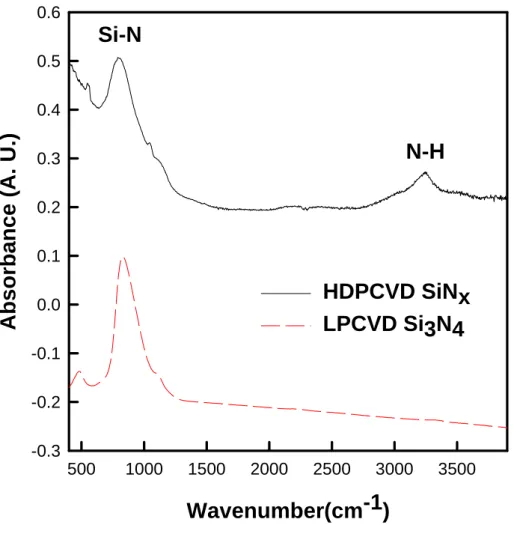
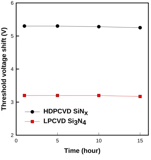
(41) furnace with SiH2Cl2 : NH3 = 30 sccm : 130 sccm. Finally, the Al gate was patterned and sintered to form a metal/oxide/nitride/oxide/silicon (MONOS) structure.. 2.3 Results and discussions. The nitride layer of a SONOS memory device is utilized to capture the injecting carriers from the channel, which cause a variation of the threshold voltage of the memory device. Figure 2-1(a) shows the band diagrams of the “write” and “erase” operation of the MONOS structure with different gate polarities. When the device is written, the electrons directly tunnel from the Si substrate through the tunnel oxide, and are trapped in the forbidden gap of the nitride layer. When the device is erased, the holes may tunnel from the valence band of the Si substrate and recombine with the electrons trapped in the nitride layer. The blocking oxide is utilized to prevent the carriers of gate electrode from injecting into the charge-trapping layer by Fowler-Nordheim (F-N) tunneling. Figure 2-1(b) exhibits the capacitance-voltage (C-V) hysteresis after the MONOS capacitor is performed by bidirectional sweeping from 12 V ~ (-12) V and in reverse. It is clearly shown in Fig. 2-1(b) that the threshold-voltage shift (memory window, ∆Vt) of the MONOS structure of the HDPCVD SiNx is prominent. The threshold-voltage shift of the HDPCVD SiNx ONO stack, 5.3 V, is considerably larger than that of the LPCVD Si3N4 ONO stack, 3.2 V, after the 12-V write operation. To lower the operating voltage, the thickness of the nitride and blocking oxide layers should be reduced at the expense of decreasing the memory window. Although the threshold-voltage shift may be lower than that depicted above, a typical sense amplifier is designed to detect the threshold-voltage differences as low as 50 mV [2.3]. With the optimization of the thickness in the gate-stacked ONO structure, the low-voltage and reliable operation, lower than 5 V, is 21.
(42) possible. The HDPCVD silicon nitride is produced in a high-density-plasma chamber with a 900-W ICP power. The rf ICP power is used to increase the spiral motion of the charged particle. A charged particle will gain more energy the more times it moves around the spiral and the high density plasma is, hence, produced [2.5]. During the deposition of the nitride layer, the simultaneously slight etching due to the bombardment of the high-density plasma is processed, which forms a densified and trap-rich silicon nitride layer [2.5-2.6]. On the other hand, the LPCVD silicon nitride is deposited in a high temperature furnace, which forms a well-bonded silicon nitride layer with fewer traps. In Fig. 2-2, Fourier transform infrared spectroscopy (FTIR) of the nitrides is schematically shown. A broadened peak of N-H bonding mode is obviously observed at the wavenumber of 3350 cm-1 in the spectrum of HDPCVD nitride rather than the LPCVD one. The hydrogenated silicon nitride is formed due to the low-temperature deposition and the hydrogen cannot be completely outgassed as the high-temperature LPCVD nitride. The trap-rich HDPCVD SiNx, therefore, results in a larger memory window (∆Vt) which is probable to make the retention characteristics meet the tolerance of 10 years. The term “retention” describes the ability of the nonvolatile memory device to store and recover information after a number of program cycles at a specified temperature [2.3-2.4]. A premise for this attention is that the leakage behavior of the memory device should be well tolerable. To maintain a good retention characteristic, the leakage current of the triple-dielectric ONO structure should be taken into account. Fortunately, as shown in Fig. 2-3, due to the well-densified silicon nitride layer [2.6-2.7], the leakage current of the HDPCVD SiNx ONO structure is slightly higher than that of the conventional LPCVD Si3N4 within an order of magnitude. The leakage characteristics are still within a quite superior range compared with conventional approach. This property makes the HDPCVD silicon nitride be a good 22.
(43) candidate to replace the conventional nitride layer for providing a larger memory window. To test the retention characteristics of our MONOS structure, a stricter environment of 150 ℃ is prepared. In Fig. 2-4, the threshold-voltage shift is measured with different periods of time when the samples are heated at 150 ℃ [2.8-2.9]. If there is any loss of the trapped charges after the 12-V write operation at 150 ℃ as time passes by, the threshold-voltage shift will gradually decrease. The ONO stack of HDPCVD silicon nitride retains a good retention property without a significant decline of the memory window up to 15 hours the same as the conventional LPCVD silicon nitride. This demonstrates the HDPCVD silicon nitride is robust to be adopted in the SONOS EEPROM technology.. 2.4 Conclusion. With the replacement of silicon nitride in the oxide/nitride/oxide (ONO) gate-stacked structure, the trap-rich HDPCVD SiNx shows a more significant threshold-voltage shift than that of the conventional LPCVD Si3N4. Also, the low-temperature (200℃) deposited HDPCVD silicon nitride shows a good retention characteristic the same as the high-temperature (780℃) LPCVD Si3N4. With the optimization of the thickness in the gate-stacked ONO structure, the low-voltage and reliable operation, lower than 5V, is realizable.. A New Method of Fabricating Superior Oxide/Nitride/Oxide Gate Stack To date, the mass produced nonvolatile memory devices are based on the concept of a continuous layer of floating gate [2.10]. However, it has faced the difficulties of 23.
(44) consecutive scaling down by the compromise between long-term nonvolatility and high operating speed [2.11]. Recently, the concept of distributed storage of charge by a nitride layer [2.12] has caught much attention. Due to the intrinsic better endurance, the absence of erratic bits, and relatively higher radiation tolerance, the silicon/oxide/nitride/oxide/silicon (SONOS) structure has emerged as the most mature nonvolatile semiconductor memory (NVSM) currently in use for space applications. The SONOS structure has a great potential of scaling the thickness of the tunnel oxide down to 1.6 nm and reducing the programming voltage below 5 volts [2.3]. Therefore, the dielectric properties of the blocking oxide, charge-trapping nitride, and tunnel oxide (ONO) gate stack are concerned. In general, the nitride layer of the SONOS structure is fabricated by LPCVD and, afterwards, the blocking oxide is deposited on the nitride layer also by LPCVD followed by a steam densification at 900 ℃ [2.13]. In this study, HDPCVD is utilized to deposit a trap-rich silicon nitride layer, followed by a high-temperature dry oxidation to form a thermally grown oxide layer on the HDP nitride layer as a blocking oxide. This new method provides a superior ONO gate stack with larger memory window and higher breakdown field compared with conventional ONO gate stack for SONOS application. First, a 2-nm-thick thermal oxide was grown at 925 ℃ on p-type (100) Si substrate by dry oxidation in an atmospheric pressure chemical vapor deposition (APCVD) furnace as a tunnel oxide. Subsequently, a 6-nm silicon nitride layer was deposited by high density plasma chemical vapor deposition on the tunnel oxide as a charge-trapping layer, followed by a dry oxidation at 982 ℃ for 30 min to form a blocking oxide layer, estimated to about 4 nm, on the nitride layer. The deposition of the HDPCVD silicon nitride was kept at 350 ℃ in a low pressure of 3 mTorr with the ratio of SiH4 : NH3 = 12 sccm : 24 sccm and an inductively coupled plasma (ICP) power of 900 W. The low pressure of 3 mTorr during deposition makes the path 24.
(45) length an electron travels without undergoing a collision with a gas atom (or mean free path) increased, which will improve the uniformity of the thin film. Differing from the prevailing SONOS technology, the blocking oxide in this study was thermally grown on the nitride layer instead of depositing on that. The oxidation was performed in APCVD at 925 ℃. Before and after the fabrication of the HDP nitride and blocking oxide, Fourier transfer infrared spectroscopy (FTIR) was utilized to investigate the quality of the HDP nitride and blocking oxide stack. After the aluminum gate electrode was patterned and sintered, the electrical measurements were performed by HP 4156 and Keithley capacitance-voltage (C-V) analyzer to examine the electrical characteristics and reliability of the ONO gate stack. Figure 2-5 exhibits the FTIR spectrum of the HDP nitride and blocking oxide stack before Al gate deposition. The absorption of sharp Si-O bonds (~1075 cm-1 and 1255 cm-1) and Si-N bonds (~820 to 900 cm-1) are clearly observed. Also, the absorption of Si-O bonds at 1255 cm-1 indicates the formation of a high quality film [2.14-2.15]. To study memory effects of the ONO sandwiched structure, a bidirectional voltage sweeping between 5 and (-5) V was performed. Figure 2-6 shows the C-V hysteresis after forward (from inversion to accumulation region) and reverse voltage sweeping (from accumulation to inversion region). When the sample is operated in positive polarity, the electrons directly tunnel from the Si substrate through the tunnel oxide, and are trapped in the forbidden gap of the nitride layer. When the device is negatively operated, the electrons may tunnel back to the Si substrate. The different threshold voltages can be defined as “1” or “0” for a memory device. The blocking oxide is utilized to prevent the carriers of gate electrode from injecting into the charge-trapping layer by Fowler-Nordheim (F-N) tunneling. In Fig. 2-6, it is also found a counterclockwise direction of the hysteresis, which implies the substrate injection of carriers rather than gate injection [2.16]. In our previous results, the 25.
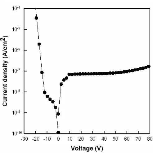
(46) trap-rich HDPCVD nitride contributes a larger threshold voltage shift, Δ Vt, (memory window) than the conventional LPCVD nitride. Under the low-voltage operation of 5 V, ΔVt is estimated to around 1.3 V which is sufficient to be defined as “1” or “0” for a memory device. Figure 2-7 shows the current-voltage (I-V) characteristics of the ONO gate stack. From the point of view of low-voltage operation, the leakage current at 5 V is considerably low under both positive bias (write) and negative bias (erase). The breakdown voltage of the ONO gate stack is about 12 V under negative bias. Dramatically, the ONO stack is operated under positive bias without breakdown up to 80 V. This feature shows a superior dielectric property for the ONO gate stack. The HDPCVD silicon nitride is produced in a high-density-plasma chamber with a 900-W ICP power. The rf ICP power is used to increase the spiral motion of the charged particle. A charged particle will gain more energy the more times it moves around the spiral and the high density plasma is, hence, produced. During the deposition of the nitride layer, the simultaneously slight etching due to the bombardment of the high-density plasma is processed, which forms a more densified silicon nitride layer than LPCVD nitride [2.6]. After the densified nitride layer is thermally oxidized, the thermally grown oxide/HDP nitride stack possesses a higher breakdown voltage than other deposited oxide/nitride stacks. The asymmetry of the leakage current at low electric field is currently under investigation. In addition, the reliability of the memory device was also investigated. As shown in Fig. 2-8, the endurance of the memory device retains an obvious memory window of 0.91 V after 106 5/(-5) V write/erase cycles. The inset exhibits the C-V hysteresis after 106 write/erase cycles. A typical sense amplifier can easily detect the threshold voltage shift of 0.91 V to define the “1” or “0” for a logic memory device. In summary, a superior ONO gate stack with a large memory window and high breakdown voltage was demonstrated. HDPCVD silicon nitride is deposited on the 26.
(47) tunnel oxide followed by a high temperature dry oxidation to form a blocking oxide layer on the nitride layer. This ONO stack with densified nitride layer and thermally grown oxide layer on the silicon nitride exhibits a reliable and viable approach for SONOS nonvolatile memory technology.. 27.
(48) (a). Write. Gate SiO2. SiNx. SiO2. Erase. 1.2. (b) 1.0. C/Cox. 0.8. 0.6. 0.4. 0.2 SiO2 / LPCVD Si3N4 / SiO2 SiO2 / HDPCVD SiNx / SiO2 0.0 -10. -5. 0. 5. Voltage (V) Figure 2-1 (a) The band diagrams of the write/erase operation of the MONOS structure with different gate polarities. The inset is the ONO gate-stacked structure in this study. (b) The C-V hysteresis of the capacitor is performed by sweeping from 12 V ~ (-12) V and in reverse. 28.
(49) 0.6. Si-N 0.5. Absorbance (A. U.). 0.4. N-H. 0.3 0.2 0.1. HDPCVD SiNx LPCVD Si3N4. 0.0 -0.1 -0.2 -0.3 500. 1000. 1500. 2000. 2500. 3000. 3500. Wavenumber(cm-1). Figure 2-2 Fourier transform infrared spectroscopy (FTIR) of the HDPCVD and LPCVD nitrides. 29.
(50) 10-7. Current density (A/cm2). SiO2 / LPCVD Si3N4 / SiO2 SiO2 / HDPCVD SiNX / SiO2. 10-8. 10-9. -4. -2. 0. 2. 4. Electric field (MV/cm). Figure 2-3 The leakage current of LPCVD and HDPCVD silicon nitride ONO gate stack. The leakage current of the HDPCVD SiNx ONO structure is slightly higher than that of the conventional LPCVD Si3N4 within an order. 30.
(51) Threshold voltage shift (V). 6. 5. 4. 3. HDPCVD SiNx LPCVD Si3N4 2 0. 5. 10. 15. Time (hour). Figure 2-4 The threshold-voltage shift versus different periods of time when the samples are heated at 150 ℃. 31.
(52) Figure 2-5 FTIR spectrum of the surface oxide layer and HDP nitride layer stack with the background spectrum of Si wafer and tunnel oxide deposited. 32.
(53) 1.0. C/Cox. 0.8. 0.6. 0.4. 0.2. 0.0 -5. -4. -3. -2. -1. 0. 1. Voltage (V). Figure 2-6 The C-V hysteresis after forward (from inversion to accumulation region) and reverse voltage sweeping (from accumulation to inversion region). 33.
(54) Figure 2-7 The current-voltage characteristics of the ONO gate stack. 34.
(55) Figure 2-8 The endurance characteristics of the memory device retains an obvious memory window of 0.91 V after 106 5/(-5) V write/erase cycles. The inset exhibits the C-V hysteresis after 106 write/erase cycles. 35.
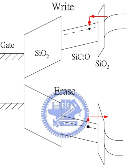
(56) Chapter 3. Memory Effect of Oxide/Oxygen-Incorporated Silicon Carbide/Oxide Sandwiched Structure. 3.1 Motivation. The Semiconductor Industry Association (SIA) International Technology Roadmap for Semiconductors (ITRS) indicates the challenge, beyond the year 2005, for nonvolatile semiconductor memories is to achieve reliable, low-power, low-voltage performance. [3.1].. In. the. area. of. electrically-erasable-programmable-read-only-memory (EEPROM) semiconductor device, there are essentially two dominant technologies which compete for an ever-expanding world market: (1) floating-gate EEPROM’s and (2) floating-trap SONOS, historically metal-insulator-SiO2-Si (MIOS), EEPROM’s. To date, the mass produced nonvolatile memory devices are based on the concept of a continuous layer of floating gate [3.2]. However, it has faced the difficulties of consecutive scaling down due to the compromise between long-term nonvolatility and high operating speed [3.3]. Recently, the concept of distributed storage of charge by an insulator, such as nitride layer, has caught much attention [3.4]. Among several kinds of MIOS memory devices, silicon nitride, as the charge-trapping insulator in the MIOS structure, is most widely used [3.5]. Other insulators are investigated to replace the silicon nitride film, such as titanium oxide, tantalum oxide, and aluminum oxide. However, these materials can not offer sufficient storage centers for the consideration of a large memory window. Therefore, the MIOS device has been made by metal ion. 36.
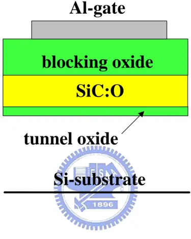
(57) implantation (e.g., Au) into SiO2 to form the interfacial charge-storage centers [3.6]. Also, to prevent the carriers from injecting into the charge-trapping insulating film from gate not from the channel, a blocking oxide is regularly used to cap on the insulator film, which forms an oxide/insulator/oxide sandwiched structure [3.7-3.8]. In this contribution, a novel metal-oxide-insulator-oxide-silicon (MOIOS) gate stack was investigated. The memory effects of the oxide/SiC:O/oxide sandwiched structure were demonstrated, which can be utilized as a high-performance MOIOS memory device.. 3.2 Experimental procedures. Figure 3-1 shows the device structure in this study. First, a 2-nm-thick thermal oxide was grown on p-type (100) 6-in Si substrate by dry oxidation in an atmospheric pressure chemical vapor deposition (APCVD) furnace as a tunnel oxide layer. Subsequently, a 20-nm SiC:O layer was deposited by high density plasma chemical vapor deposition (HDPCVD) on the tunnel oxide as a charge-trapping layer, followed by the deposition of a 20-nm HDPCVD silicon dioxide as the blocking oxide. A steam densification at 982 ℃ was also performed for 180 sec to densify the blocking oxide [3.8]. The deposition of the SiC:O film was kept at 350 ℃ in a low pressure of 3 mTorr with precursors of SiH4, CH4 and O2 and an inductively coupled plasma (ICP) power of 900 W. The parameters of the deposition of the SiC:O film are listed in Table 3-1. This study was divided into three samples. The deposition of SiC:O with least oxygen content (2 sccm) was defined as sample 1. From sample 1 to sample 3, the content of oxygen was increased with a decreased refractive index. The low pressure of 3 mTorr during deposition makes the path length an electron travels without undergoing a collision with a gas atom (or mean free path) increased, which 37.
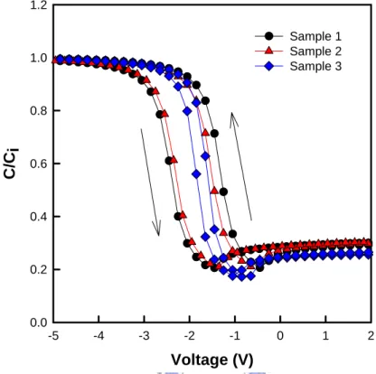
(58) will improve the uniformity of the thin film [3.9]. The blocking oxide was deposited at 350 ℃ with the ration of SiH4 : N2O = 6 sccm : 150 sccm and a 900-W ICP power. Finally, the Al gate electrode was patterned and sintered to form a MOIOS structure.. 3.3 Results and discussions. To study memory effects of the oxide/SiC:O/oxide sandwiched structure, a bidirectional voltage sweeping between 7 and (-7) V was performed. Figure 3-2 shows the capacitance-voltage (C-V) hysteresis in this study for different samples. It is clearly observed that as the content of oxygen is increased, the threshold voltage shift (memory window) is decreased from sample 1 to sample 3. The memory window of sample 1 is estimated to be about 1.1 V under 7-V operation. In Fig. 3-3, the band diagrams of the “write” and “erase” operation are exhibited. When the MOIOS structure is operated under positive polarity, the electrons directly tunnel from the Si substrate through the tunnel oxide, and are trapped in the forbidden gap of the SiC:O layer. When the device is negatively operated, the electrons may tunnel back to the Si substrate through tunnel oxide. The different threshold voltages before and after programming can be defined as “1” or “0” for a memory device. The blocking oxide is utilized to prevent the carriers of gate electrode from injecting into the charge-trapping layer by Fowler-Nordheim (F-N) tunneling. HDPCVD SiC:O is produced in a high-density-plasma chamber with a 900-W ICP power. The rf ICP power is used to increase the spiral motion of the charged particle. A charged particle will gain more energy the more times it moves around the spiral and the high density plasma is, hence, produced [3.9]. During the deposition of the carbide layer, the simultaneously slight etching due to the bombardment of the high-density plasma is processed, which forms a densified and trap-rich layer and contributes a larger 38.
數據

+7
相關文件
• The memory storage unit is where instructions and data are held while a computer program is running.. • A bus is a group of parallel wires that transfer data from one part of
a substance, such as silicon or germanium, with electrical conductivity intermediate between that of an insulator and a
• The memory storage unit holds instructions and data for a running program.. • A bus is a group of wires that transfer data from one part to another (data,
Seals, if any, essential for sealing the pressure sensing element, and in direct contact with the process medium, made of or protected by aluminum, aluminum alloy, aluminum
• To introduce the use of the LPF as a tool for planning the school English Language curriculum; and
Understanding and inferring information, ideas, feelings and opinions in a range of texts with some degree of complexity, using and integrating a small range of reading
Numerical experiments are done for a class of quasi-convex optimization problems where the function f (x) is a composition of a quadratic convex function from IR n to IR and
Chen, The semismooth-related properties of a merit function and a descent method for the nonlinear complementarity problem, Journal of Global Optimization, vol.. Soares, A new
A “charge pump”: a device that by doing work on the charge carriers maintains a potential difference between a pair of terminals.. Æan emf device
