國立交通大學
電機學院 電子與光電學程
碩 士 論 文
在閉迴路上使用資料相位校正器之
10-Gb/s CMOS
時脈與資料回復電路
A 10-Gb/s CMOS Clock and Data Recovery Circuit
with Data-Deskew Buffers in the Closed Loop
指導教授:蘇朝琴 周世傑 教授
研 究 生:楊忠傑
10-Gb/s CMOS
時脈與資料回復電路
A 10-Gb/s CMOS Clock and Data Recovery Circuit
with Data-Deskew Buffers in the Closed Loop
研 究 生: 楊忠傑 Student : Chungchieh Yang
指導教授: 蘇朝琴 教授 Advisors : Dr. Chauchin Su
周世傑 教授 Dr. Shyhjye Jou
國 立 交 通 大 學
電機學院 電子與光電學程
碩士論文
A ThesisSubmitted to College of Electrical and Computer Engineering National Chiao Tung University
in partial Fulfillment of the Requirements for the Degree of
Master of Science in
Electronics and Electro-Optical Engineering September 2007
Hsinchu, Taiwan, Republic of China
10-Gb/s CMOS
時脈與資料回復電路
研究生 : 楊忠傑 指導教授 : 蘇朝琴 教授
周世傑 教授
國立交通大學 電機學院 電子與光電學程碩士班
摘 要
本篇論文提出一個適用於晶片上多通道之資料校正(data-deskew)時脈與資 料回復(CDR)電路。 此 CDR 系統是藉由調整數位控制延遲線(DCDL)內的資料延遲量來回復單通 道 10-Gb/s 之突發資料封包。在最佳選取點獲取之後,資料週期的中點會對準時 脈的選取邊緣,同時由通道所造成的偏移也獲得補償。 此 CDR 是一階系統,因此本質上就是穩定的。在傳送和接收端最大時脈抖動 差量合於規範的前提下,它可以鎖定的頻率誤差為 1000 ppm。又,閉迴路的特 性使得此系統內之抖動為一低通模式。 所有的電路方塊均採用數位電路的實現方式。透過可信度計數器內部所採用 之多數決(majority-vote)方式來達到快速鎖定(平均為 110 個位元時間)。在此 系統中存在兩個關鍵設計:1)是高速、大擺幅之 CMOS 延遲線設計,2)是滿足迴 路延遲之設計條件。 此外,這篇論文使用 TSMC 0.13-μm CMOS 製程,實現了一個 10-Gb/s 的數 位傳接器。 索引詞彙─高速序列化傳輸鏈,CMOS 傳接器,時脈與資料回復,延遲鎖定迴 路,鎖相迴路,數位控制延遲線,相位校正緩衝器,可信度計數器。with Data-Deskew Buffers in the Closed Loop
Student: Chungchieh Yang Advisors: Dr. Chauchin Su
Dr. Shyhjye Jou
Degree Program of Electrical and Computer Engineering
National Chiao Tung University
Abstract
This thesis proposes a data-deskew clock and data recovery (CDR) architecture for the on-chip multi-channel timing recovery.
This CDR recovers the 10-Gb/s/ch burst data packet by adjusting the data delay in the digitally controlled delay line (DCDL). After the acquisition of the optimal sampling phase, the midpoint of data period aligns to the sampling clock. The data skew between channels is also compensated.
This CDR is first-order and therefore inherently stable. It can track the specified 1000-ppm frequency error as long as the peak-to-peak clock jitter between the transmitter and the receiver sites is confined to the specification. And, the closed loop characterizes the high-band-limited jitter in this system.
All building blocks adopt digital circuits. Fast acquisition (110-bit time in typical case) is achieved by the majority-vote scheme in the confidence counter. Two critical designs exist in this digital-circuit CDR: 1) high-speed large-swing CMOS DCDL deign, and 2) meeting the loop-latency constraint.
In addition, a digital implementation of the 10-Gb/s transceiver is realized in TSMC 0.13-µm CMOS technology.
Index Terms─High-speed serial links, CMOS transceivers, clock and data recovery, delay-locked loops, phase-locked loops, digitally-controlled delay lines, deskew buffers, confidence counters.
誌 謝
由衷感謝 蘇朝琴教授與 周世傑教授兩位老師,在個人遲來的學生生涯中給 予指導以及教誨。尤其感謝蘇老師帶我進入高速序列化傳輸的領域,除了授予電 路設計的知識,並教我做人處事更圓融。 也感謝交通大學在職專班提供的升學途徑。從前在業界做中學,系統與電路 多要靠自己摸索。「能夠在校園內接受正規的訓練,是一件相當幸福的事。」 希望將這份喜悅與我的父母家人分享,感謝您們長久以來的支持與付出。還 有感謝我的女友 stella,多年的陪伴與鼓勵。 另外,感謝鴻文在學業上無私的指點與協助;感謝仁乾,在困頓的時候與你 談話總能帶來安慰。感謝丸子照料實驗室的大小事,讓我們的學習沒有了後顧之 憂。還有謝謝盈杰,諸多生活瑣事向你請益總能得到完滿的答覆。 文末,祝福 918 實驗室的學長、同學與學弟妹們,祝福每個人都能找到屬於 自己的一片天空。 楊忠傑 Sep 2007Table of Contents
Abstract ... viii
Table of Contents ...x
List of Figures ...xii
List of Tables...xv
Chapter 1 Introduction ...1
1.1 Motivation...1
1.2 Features ...3
1.3 Organization...3
Chapter 2 Overview of the World’s CDR Architectures...5
2.1 PLL-Based CDR ...6
2.2 Blind Oversampling CDR...8
2.3 DLL-Based CDR ...10
2.4 Gated-VCO CDR ...14
2.5 Alternative & Hybrid ...16
2.6 Summary ...19
Chapter 3 Deskew CDR: System-Level Analysis...21
3.1 System Architecture ...21 3.2 System Specifications ...23 3.3 Design Parameters ...23 3.4 Multi-Channel Synchronization...30 3.5 Behavioral Models ...31 3.6 Behavioral Simulations...36
Chapter 4 Deskew CDR: Circuit Implementation ...42
4.1 System Architecture ...42
4.2 Critical Design (1): DCDL...43
4.3 Critical Design (2): Loop Latency ...49
Chapter 5 A 10-Gb/s Transceiver Test Chip ...62
5.1 Architecture...62
5.2 Design for Test ...63
5.3 Building Blocks ...67
Chapter 6 Layout & Post Simulations ...71
6.1 Layout ...71 6.2 Post Simulation ...76 6.3 Test Environment ...81 Chapter 7 Conclusion...83 7.1 Specification Table...84 7.2 Comparison ...85 Bibliography ...87
List of Figures
Fig. 1.1: Multi-channel timing recovery by multiple Deskew CDRs ...2
Fig. 2.1: A generic PLL-based CDR with a charge pump ...6
Fig. 2.2: Jitter peaking phenomenon...7
Fig. 2.3: The PLL-based CDR, Savoj2001 ...8
Fig. 2.4: The PLL-based CDR, Savoj2003 ...8
Fig. 2.5: A generic oversampling CDR, Kim&Jeong2003 [13]...9
Fig. 2.6: The blind oversampling CDR, C.K.Yang98 ...9
Fig. 2.7: The clock-interpolation CDR, E.Lee2001... 11
Fig. 2.8: The clock-interpolation CDR, Kreienkamp2005 ...12
Fig. 2.9: The data-deskew CDR, Wong96 (a) Architecture (b) Edge Detector ...13
Fig. 2.10: The data-deskew CDR, Lu2005 ...13
Fig. 2.11: Gated-VCO CDR, Nakamura96 (a) architecture (b) gating circuit...14
Fig. 2.12: Gated-VCO CDR, Nogawa2005 ...15
Fig. 2.13: Gated-VCO CDR, Kaeriyama2003 ...16
Fig. 2.14: FSM-based CDR, Analui2005 (a) Architecture (b) State Diagram at n=2..17
Fig. 2.15: Semi-blind oversampling CDR, Ierssel2006...18
Fig. 2.16: DLL & DLL/PLL CDR, T.Lee92 ...19
Fig. 2.17: Mixed PLL/DLL, Bae&Wei2004 ...19
Fig. 3.1: Deskew CDR system architecture ...22
Fig. 3.2: (a) Avg. required delay (25ps) (b)4-bit time transition probability...24
Fig. 3.3: Data eye diagram with the sampling clock...25
Fig. 3.4: Jitter models of a) the uniform distribution b) Gaussian distribution ...25
Fig. 3.5: Simulation of frequency tolerance (a) the main plot (b) a zoom-in version .27 Fig. 3.6: Multi-channel data recovery (a) aligning case (b) shifting 1-bit case ...30
Fig. 3.7: Deskew CDR system architecture in Simulink ...31
Fig. 3.8: Data generator & DCDL in Simulink...32
Fig. 3.9: Adding noise sources in Simulink (a) a reference eye (b) ISI effect (c) random noise (d) the combination of ISI and random noise...33 Fig. 3.10: Jitter histogram plots of (a) ISI (b) Random noise (c) ISI and Random noise
Fig. 3.11: Phase detectors’ block in Simulink...34
Fig. 3.12: Confidence Counter in Simulink ...35
Fig. 3.13: Simulations of random noise (a) free of random noise (b) 0.2-UI random noise (c) 0.4-UI random noise ...37
Fig. 3.14: Simulations of loop latency ...38
Fig. 3.15: Simulations of frequency error (a) free of frequency error, (b) 300-ppm frequency error at TX, (c) 500-ppm frequency error at TX...40
Fig. 3.16: Simulation of DCDL’s overflow...40
Fig. 4.1: Deskew CDR circuit-level architecture...43
Fig. 4.2: DCDL architecture ...45
Fig. 4.3: Schematics of (a) a delay cell (b) MUX4:1 (c) the interpolator...45
Fig. 4.4: Schematics of (a) the proposed inductive peaking, (b) an inductive- peaking folded amplifier in half circuits, (c) the inductive load. ...47
Fig. 4.5: Simplified small-signal model of the proposed inductive peaking ...48
Fig. 4.6: The loop-latency timing ...50
Fig. 4.7: The timing diagram: from PDs to the 3-bit encoders ...51
Fig. 4.8: Conventional APD (a) schematic (b) data leads (c) data lags ...52
Fig. 4.9: Proposed APD (a) schematic (b) timing diagram...52
Fig. 4.10: Confidence counter architecture...53
Fig. 4.11: The 3-bit binary comparator ...54
Fig. 4.12: Circuits of look-ahead carries...55
Fig. 4.13: The main counter in the accumulator ...55
Fig. 4.14: T’s logic in pseudo-NMOS...56
Fig. 4.15: The state transition diagram of the accumulator ...56
Fig. 4.16: The 5-bit counter in FSM ...57
Fig. 4.17: NOR gates for coarse control (a) NOR3 (b) NOR2 ...59
Fig. 4.18: The circuit of Y = ⊕ ⋅ for the fine control...60 A (B C) Fig. 4.19: (a) XOR (b) XNOR ...60
Fig. 4.20: Schematics of (a) a DFF, (b) master & slave latches, (c) a latch, (d) the source-coupling latch. ...61
Fig. 4.21: Schematics of (a) a resetable TFF, (b) master & slave stages of the TFF, (c) the circuit of MUX & latch...61
Fig. 5.2: Bypass-mode operation ...65
Fig. 5.3: Nominal operation ...65
Fig. 5.4: Debug-mode operation ...66
Fig. 5.5: A 3-stage Johnson counter (a) architecture (b) timing diagram ...67
Fig. 5.6: The multi-phase clock generator ...68
Fig. 5.7: The 10-Gb/s 4-to-1 Serializer ...69
Fig. 5.8: The 10-Gb/s output buffer (a) architecture (b) binary-control tri-state buffers ...70
Fig. 6.1: Source-coupling pairs in the delay cell ...72
Fig. 6.2: Source-coupling pairs in the latch ...72
Fig. 6.3: Common-centroid scheme (a) m = 2 (b) m = 3 (c) m = 4 ...73
Fig. 6.4: Grid design (a) power grid (b) Cap1 (c) Cap2 ...74
Fig. 6.5: Chip Layout ...74
Fig. 6.6: Deskew CDR (a) layout (b) block layout with I/O ports...75
Fig. 6.7: The bonding pad model ...76
Fig. 6.8: DCDL post simulation (a) phase resolution (b) tuning range ...77
Fig. 6.9: DCDL worst-case setup...78
Fig. 6.10: DCDL post simulation - worst eye diagrams ...78
Fig. 6.11: Deskew CDR post simulation...79
Fig. 6.12: Deskew CDR post simulation – FSM ...80
Fig. 6.13: Full-chip post simulation...81
Fig. 6.14: 10-Gb/s output eyes (a) single-ended To (b) differential-ended To-Tob ...81
Fig. 6.15: Test environment ...82
List of Tables
Table 1: CDR architectures summary ...20
Table 2: Specifications of the 10-Gb/s Deskew CDR...23
Table 3: The loop bandwidth fBW vs. the input jitter amplitudeA ...28 j Table 4: MOS intrinsic f in TSMC 0.13-µm 1P8M technology ...46 T Table 5: The truth table of the proposed APD ...53
Table 6: The truth table of the encoder ...54
Table 7: The state table of the accumulator ...57
Table 8: The truth tables of FSM (a) coarse tuning function (b) fine tuning function.58 Table 9: The complete truth tables of FSM...58
Table 10: Pads and power configurations ...74
Table 11: Block layout area...75
Table 12: The ports information of the CDR (a) internal ports (b) external ports ...76
Table 13: DCDL phase resolution and tuning range...77
Table 14: DCDL output peak-to-peak jitter at the worst-case setup...78
Table 15: DCDL Specifications ...84
Table 16: Deskew CDR Specifications...85
Chapter 1
Introduction
1.1 Motivation
SoC (system-on-chip) has become an industrial trend to provide a solution of both high performance and low power consumption. As CMOS technology advances rapidly, die size of couple centimeters and gate count of more than hundreds of million have been brought to the reality. High-throughput data communication is demanding.
A high-speed serial link transports serialized data stream from the near site to the far site. It is a common way to save the routing cost of the low-speed parallel channels. As the computing/processing capability of a digital system is greatly improved by the advancing technology, the finite bandwidth of a single serial link may no longer meet the required bandwidth. It is necessary to apply parallelism back to the serial links.
The performance of these serial links turns out to be the performance metric of the entire system.
burst-mode timing recovery, and is implemented with digital circuits. It adjusts the delay of the data by deskew buffers and aligns the midpoint of a data period to the clock so as to recover the data synchronously. It is called a data-deskew CDR, or simply Deskew CDR. … … … … … … … … Deskew CDR Ch0 Data Ch1 Data Ch2 Data Deskew CDR Deskew CDR …… …… …… Ch(n-1) Data Deskew CDR SER SER SER SER SER SER SER SER …… Ch0 Di Ch1 Di Ch2 Di Ch(n-1) Di Ch0 Di Ch1 Di Ch2 Di Ch(n-1) Di .. .. Multi-phase Clocks from PLL @ TX Multi-phase Clocks from PLL @ RX Ch0 Do Ch1 Do Ch2 Do Ch(n-1) Do Ch0 Do Ch1 Do Ch2 Do Ch(n-1) Do
…
…
…
Fig. 1.1: Multi-channel timing recovery by multiple Deskew CDRs
Multiple Deskew CDRs target on multi-channel timing recovery. Fig. 1.1 shows n-channel timing recovery by n sets of Deskew CDRs. Data skews between channels consist of static and dynamic components. The illustrated channel routing mismatch refers to the static aspect. And, driving source mismatch, substrate noise under channels, electromagnetic interference during transmission, etc refer to the dynamic aspect. Deskew CDRs compensate the total data skews between channels, and accomplish the timing recovery.
Fig. 1.1 also shows the environment setup for multiple links. A single PLL located at the transmitter site (TX) provides multi-phase clocks to serializers. Another PLL located at the receiver site (RX) provides multi-phase clocks to the CDRs. The clock jitter between PLL at TX and PLL at RX is specified, and it refers to the tuning range of digitally controlled delay line (DCDL) directly.
These two PLLs introduce a relatively simple environment for multi-channel timing recovery, as compared to that of conventional PLL-based CDRs.
1.2 Features
The 10-Gb/s Deskew CDR is a first-order recovering system, and therefore it is inherently stable. High-frequency jitter is filtered because of the loop filter. There is no jitter accumulation due to the absence of
( )
1/s from an oscillator inside the loop. A first-order system intends to track the phase error. Still, it can track the frequency error between TX and RX to some extent.All the building blocks adopt digital circuits for design robustness, since digital circuits benefit more from the scale-down technology than most analog circuits. Besides, analog circuits, such as the conventional charge pump and the passive R-C filter, still suffer from the matching issue. In this work, a digital confidence counter serves as the loop filter to the CDR. Fast acquisition is achieved by the majority vote scheme, which is implemented as a comparator inside the confidence counter.
Deskew CDR focuses on the design of DCDL. The high-speed large-swing CMOS delay line provides the monotonic delay adjustment. A tuning range of more than 1.4 UI is achieved in this work. Static CMOS inverters compose the main delay stages for the delay line. Large noise margin is guaranteed by the large-swing behavior and also by the hysteresis characteristic of the delay cell.
A wider tuning range can be achieved under a lower supply as long as the DCDL-induced jitter meets the specification. As the supply gets lower, the crossing point of the delayed data is self-adjusted due to the balanced pull-up/pull-down CMOS inverter.
Besides, an implementation of the 10-Gb/s transceiver in TSMC 0.13-µm CMOS technology is demonstrated in this work.
1.3 Organization
This dissertation comprises seven chapters. The motivation and features of the CDR are described in this chapter.
Chapter 2 gives an overview of the world’s CDR architectures, which is far beyond the PLL-based and the oversampling architectures. It describes the operation principles, the issues, and discovers the possibilities on various architectures.
Chapter 3 analyzes the system-level behaviors of the CDR. Topics on system specifications, design parameters, and simulations are involved. Discussions and simulations on various cases, such as noise profiles, the frequency tolerance, the loop
latency, and the frequency error, can be found in this section.
Chapter 4 depicts the circuit-level implementation. The high-speed large-swing
DCDL design and meeting the loop-latency constraint are described. To minimize the
loop latency, the pseudo-NMOS scheme is adopted. Demonstrated can be found in the carry-look-ahead adder of the comparator, or the TFF up-down counters of the confidence counter and the FSM.
Chapter 5 shows the digital implementation of the 10-Gb/s transceiver. It describes the considerations for design and test, as well as different operation modes. The CDR is verified in nominal mode and/or debug mode, while the phase resolution of DCDL is measured in bypass mode. The multi-phase clock generator, the serializer, and the 10-Gb/s output buffer are also discussed in this section.
In the high-speed domain, the circuit layout is critical and dominates the final eye open. Chapter 6 shows the chip layout, grid design, and describes the layout guidelines for high-speed circuits. The guideline of source coupling is especially emphasized. Post simulations of DCDL, the CDR, and the full-chip transceiver are given in this section.
The final section, Chapter 7, shows the specification table of Deskew CDR. It compares the power/area among several CDR systems.
Chapter 2
Overview of the World’s
CDR Architectures
Different applications require different CDR systems to the world. The types of CDR systems reflect on the modes of recovering process: continuous vs. burst, closed loop vs. open loop, filter-based vs. oversampling, clock delay vs. data delay, and digital vs. analog, and etc.
For conventional CDR systems, we have PLL-based and oversampling CDR architectures. They are well-explored and have their own traditions. But there are more candidates for applications of the timing recovery. Following the classification
in [1]1, we categorize CDR systems into 1) PLL-Based, 2) Blind Oversampling, 3)
DLL-Based, 4) Gated VCO, and 5) Alternative & Hybrid architectures.
In this section, some of the demonstrated systems are history, while some of them are state-of-the-art. This section mainly focuses on the world-view, the variety, and the possibilities of CDR systems.
1
A presentation document introduces the world’s CDR systems on the internet by Çobanoğlu in 2006. The original classification is 1) PLL-Based, 2) Delay-the-Data, 3) Gated VCO, 4) (Semi-)Blind Oversampling, and 5) FSM-Based.
2.1 PLL-Based
CDR
PLL-based CDR systems are suitable for continuous mode operation. They can be characterized as single loop [3]-[5] and dual loop [6]-[9]. In general, a PLL-based CDR system refers to an Nth-order system, where N≥2. It is usually implemented with analog circuits due to the inherently continuous characteristics.
Di RetimeRetimeRetime DoDo
P/F Detector
Charge Pump
VCO LPF
Fig. 2.1: A generic PLL-based CDR with a charge pump
Fig. 2.1 shows a generic PLL-based CDR architecture. It consists of phase and/or frequency detectors, a charge pump, a loop filter, and a VCO. For the dual-loop architecture, the entire recovery process includes the slow pull-in process by frequency detectors and then the lock-in process by phase detectors in sequence.
Back to 1985, a PLL-based system [3] was proposed for clock and data extractions from NRZ data. It employs an active SAW filter in the loop for the band-pass filtering instead of the architecture with a charge pump and a passive filter. After the charge pump becomes popular, a second-order low-pass filter of ‘C // R-C’ structure is also welcome [5], [8]. The second-order filter composes a third-order system, so that phase step, frequency step, as well as the accelerative frequency variation can be tracked.
A high-order PLL-based system is well known as its high performance. However, it doesn’t suit burst-mode applications because of 1) the slow pull-in process, and 2) clock drifting at the case of no input.
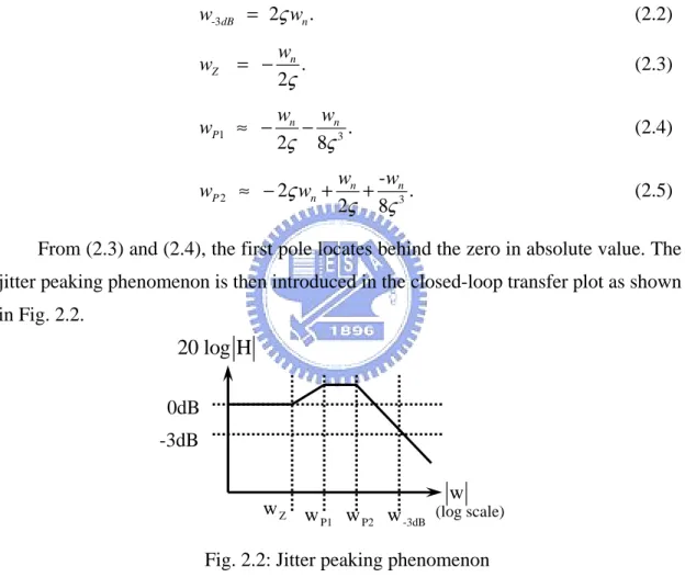
Besides, there exists jitter peaking phenomenon [2] in the high-order system. To take the simplest case for instance, consider a second-order system. The closed-loop transfer function is expressed in (2.1).
2 2 2 2 ( ) , 2 2 . 2 n n n n n n w s w H s s w s w w s w ς ς ς ς + = + + ≈ + (2.1)
The approximation of (2.1) is made by assuming that damping factor ς is large (such as 10) and w n2 is small enough and can be neglected. The approximated loop
bandwidth is then derived in (2.2). And the corresponding zero and poles are given in (2.3)-(2.5). -3dB 2 n. w = ςw (2.2) . 2 n Z w w ς = − (2.3) 1 3. 2 8 n n P w w w ς ς ≈ − − (2.4) 2 3 -2 . 2 8 n n P n w w w ςw ς ς ≈ − + + (2.5)
From (2.3) and (2.4), the first pole locates behind the zero in absolute value. The jitter peaking phenomenon is then introduced in the closed-loop transfer plot as shown in Fig. 2.2.
Fig. 2.2: Jitter peaking phenomenon
The jitter peaking J is P
2 1/ 1 1/4 . P P Z J = w w ≈ + ς (2.6) To express (2.6) in dB, we get 2 8.686 ln(1 1/ 4 ) dB. P J ≈ + ς (2.7)
The amount of jitter peaking in (2.7) can be eliminated by over-damping the loop; that is applying large ς . But it results in slow response of the lock acquisition.
w 20 log H 0dB Z w P1 w -3dB P2 w w-3dB (log scale)
Example: Savoj2001 [4] 10Gb/s Di 5-GHz VCO Charge Pump LPF Half-Rate PD SER 10Gb/s Do 10Gb/s Di 5-GHz VCO Charge Pump LPF Half-Rate
PD SERSERSER 10Gb/s Do10Gb/s Do
Fig. 2.3: The PLL-based CDR, Savoj2001
Example: Savoj2003 [6] Loop Filter 10Gb/s Di Retimed 10Gb/s Do Half-Rate FD Half-Rate PD V/I Converter V/I Converter 0 45 90 135 0 45 90 135 VCO
Fig. 2.4: The PLL-based CDR, Savoj2003
2.2 Blind
Oversampling
CDR
A blind oversampling architecture, shown in Fig. 2.5, is implemented with digital circuits, and can handle both continuous and burst-mode timing recovery. It oversamples the data and chooses the optimal clock phase according to the extracted edges information in decision circuit. The decision scheme can be either majority-voting [10] or center-picking [11], while the previous is less superior. [12]
Multi-phase Clock Generator Parallel Samplers Sample Storage MUX Decision Circuit Di
. .
Do.
. .
.
Multi-phase Clock Generator Parallel Samplers SampleStorage MUXMUX
Decision Circuit
Di
. .
Do.
. .
.
Fig. 2.5: A generic oversampling CDR, Kim&Jeong2003 [13]
A blind oversampling CDR tracks the high-frequency jitter of input data stream well, while the limited size of storage causes a limitation on tracking the low-frequency jitter.
Different from most CDR systems, this architecture eliminates the need on the acquisition time but requires extra hardware for executing algorithm and introduces processing latency to the data recovery.
The phase picking scheme accompanies static offset error on each sampling, because neither the data nor the clock phases are adjusted. The maximum offset error is (0.5 UI / OSR) , where OSR denotes the oversampling ratio. Although this offset error can be suppressed by raising the oversampling rate, but in practical cases it encounters issues like: 1) A high OSR implies high-accuracy phase resolution for each sampling, which is always a challenge. 2) The input capacitance of phase detectors grows with OSR. That is especially critical to high-speed application. In the conventional way, 3×-oversampling is widely-used.
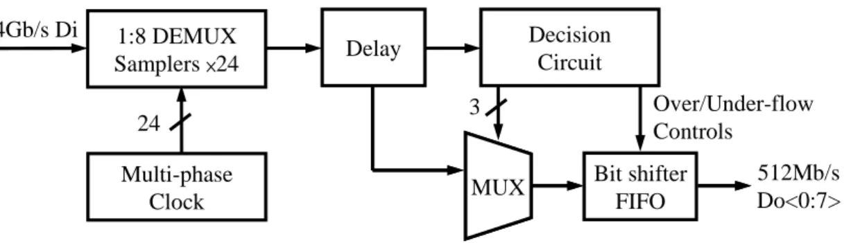
Example: C.K.Yang98 [14] 24 MUX MUX 512Mb/s Do<0:7> 4Gb/s Di 1:8 DEMUX Samplers ×24 Bit shifter FIFO Over/Under-flow Controls Decision Circuit Multi-phase Clock Delay 3
In Fig. 2.6, the sample storage is denoted as a delay block, and the decision circuit controls the multiplexer as well as the FIFO at the last stage. The FIFO is implemented with an 8-bit shifter. It handles both the overflow and underflow cases when the phase error, which is mainly caused by the frequency error, accumulates more than 1-bit time.
2.3 DLL-Based
CDR
A DLL-based CDR can be regarded as a simplified version of PLL-based architecture. It is a closed-loop first-order system without jitter peaking phenomenon. In this system, only the phase delay is a variable. Implementations of DLL-based CDR can be either analog or digital, while the latter is the major trend in recent days.
According to the subject of delay adjustment, it can be distinguished as 1) clock-interpolation, and 2) data-deskew architectures. The clock-interpolation architecture can handle continuous timing recovery by the phase-rotation scheme, but this phase rotation needs additional hardware, such as the FIFO stage of oversampling architecture in Fig. 2.6, to handle the overflow/underflow condition.
As for the data-deskew architecture, it is a straight concept to adjust data instead of clock. It introduces a simple synchronization behavior by the shared and untouched global clock. But it is mainly limited by the data tuning range, and therefore is only suitable for burst-mode applications.
2.3.1 Clock-Interpolation
CDR
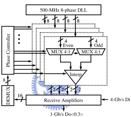
Fig. 2.7 shows an example of clock-interpolation CDR by E. Lee. The 8 clock phases are adjusted by the interpolation scheme, which is generated from the phase controller, and finally the sampling clock phases align to the midpoint of data duration. The receive amplifiers block consists of amplifiers and phase detectors. Here the full-rate data is de-multiplexed into 4 quarter-rate data inherently. Even though digital circuits implement the logic function in the phase controller block, the entire CDR implementation also adopts analog circuits.
Fig. 2.8 shows a clock-interpolation CDR for multi-channel timing recovery by Kreienkamp. It adopts analog circuitry to achieve high speed and fine phase resolution. Differential charge pump and two capacitors contribute the single pole to
the system. The phase interpolator is the conventional analog current-steering scheme, and just like those PLL-based CDR systems, the phase resolution is limited by the discrete steps, which is introduced by charge pump. The chip is fabricated in 0.11-µm CMOS technology, and its power consumption is 220-mW at a supply of 1.5 Volt.
But for continuous recovery, it lacks of description about phase-rotation of these CDR macro-cells. Example: E.Lee2001 [15] 2 2 2 2 2 2 2 2 Even Odd Interp MUX 4:1
MUX 4:1 MUX 4:1MUX 4:1
DE MUX 4 4 44 Receive Amplifiers 16 16 4-Gb/s Di 1-Gb/s Do<0:3> 8 500-MHz 8-phase DLL 8 8 8 8 8 8 8 8 P h ase Co n tr o lle r
...
Fig. 2.7: The clock-interpolation CDR, E.Lee2001
Example: Kreienkamp2005 [16] Phase Detectors Interp Charge Pump & PI-Ctrl 2 2 DEMUX 2 : 4 2.5-Gb/s Do<0:3> Up, Dn 2 Pre-Amp Low-Pass Filter CKI CKQ 10-Gb/s Di DetectorsPhase Interp Charge Pump & PI-Ctrl 2 2 2 2 DEMUX 2 : 4 DEMUX 2 : 4 2.5-Gb/s Do<0:3> Up, Dn 2 2 Pre-Amp Low-Pass Filter CKI CKQ 10-Gb/s Di (a)
CDR Shared PLL CDR CDR CDR Multi-channel Recovery Recovered Data Input Data
…
…
CDR Shared PLL CDR CDR CDR Multi-channel Recovery Recovered Data Input Data…
…
Clock (b)Fig. 2.8: The clock-interpolation CDR, Kreienkamp2005 (a) the CDR, (b) the multi-channel configuration
2.3.2 Data-Deskew
CDR
Fig. 2.9(a) shows the 10-Gb/s data-deskew CDR for multi-channel burst-mode applications proposed by Wong. It is a full-rate analog implementation, and fabricated
in both AlGaAs/GaAs and InGaP/GaAs HBT technology, where f ~ 50 GHz , t
max
f ~ 60 GHz and ~ 40β . The voltage controlled delay line, phase detector, and loop filter compose the delay lock loop. In addition, it employs an edge detector circuit to adjust the time constant of the loop filter. Fig. 2.9(b) shows the phase detector circuit. The detector’s output is generated from the transition edge of input and its asynchronous delay.
The achieved tuning range is 2 UI or 200 ps. It claims to be capable of a 12.5-kbit data packet but under the assumption that frequency error for all clocks is within 20 ppm. The 20-ppm error is far less than the conventional estimation of 200 ppm.
Fig. 2.10 shows a digital implementation of data-deskew CDR by Lu. The confidence counter replaces the conventional loop filter. The cascaded delay cells compose the DCDL block. Coarse and fine tune functions are available. The coarse function is implemented by the on/off state of tri-state buffers in the chain, and the fine function is implemented by the added amount of capacitive load.
It is fabricated in 0.18-µm CMOS technology, and the achieved tuning range is 1 UI, or 400 ps, for the 2.5-Gb/s operation. Due to the insufficient tuning range, this implementation is not going to handle any frequency error.
Example: Wong96 [17] Voltage Controlled Delay Line Phase Detector Loop Filter Data Retime Edge Detector 10-Gb/s Di 10-GHz Clock 10-Gb/s Do (a) Out Envelope Detector In Out Envelope Detector In (b)
Fig. 2.9: The data-deskew CDR, Wong96 (a) Architecture (b) Edge Detector
Example: Lu2005 [18] Phase Detector Confidence Counter Delay Control FSM Up Dn Lead Lag
Digitally Controlled Delay Line
5-GHz Clock 2.5-Gb/s Di 2.5-Gb/s Do
...
2.4 Gated-VCO
CDR
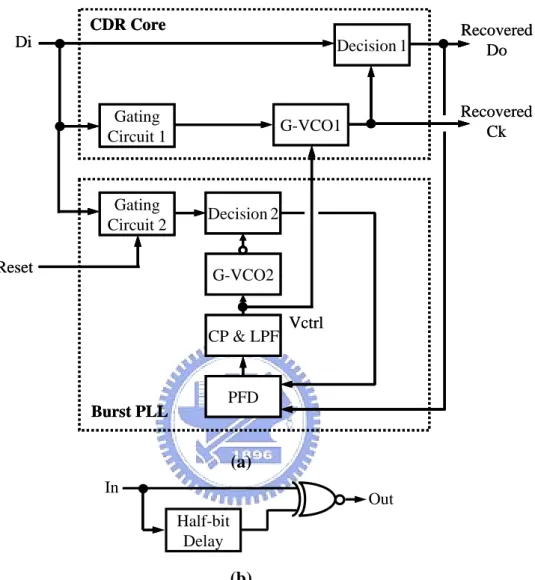
Example: Nakamura96 [19] CDR Core Gating Circuit 1 G-VCO1 G-VCO2 CP & LPF PFD Burst PLL Recovered Do Recovered Ck Vctrl Decision 1 Di Decision 2 Gating Circuit 2 Reset CDR Core Gating Circuit 1 G-VCO1 G-VCO2 CP & LPF PFD Burst PLL Recovered Do Recovered Ck Vctrl Decision 1 Di Decision 2 Gating Circuit 2 Reset (a) Half-bit Delay In Out (b)Fig. 2.11: Gated-VCO CDR, Nakamura96 (a) architecture (b) gating circuit
A gated-VCO CDR system was first introduced by Nakamura in 1996. It can fast response to the asynchronous burst input data. In Fig. 2.11(a), the CDR core consists of a gating circuit, a gated VCO, and a DFF at the final stage for retiming the data. This DFF is denoted as Decision 1 block.
The gating circuit in Fig. 2.11(b) adopts the same scheme as that in Fig. 2.9(b). It detects the transition edge of input data. Consider the gating signal is logic 0, and the Vctrl signal is ready; the gated VCO oscillates by default and is ready to re-initiate an oscillation. As the gating signal validates, the gated VCO re-generates the gated clock instantaneously. In other words, the gating signal re-synchronizes the gated clock,
every time the data transition validates.
This prototype of gated-VCO architecture cooperates with a burst PLL, which provides the control voltage to the CDR. An additional reset action is required after each burst data recovery.
Example: Nogawa2005 [20] CDR Core Gating Circuit DFF G-VCO1 Input Amp. G-VCO2 CP & LPF PFD ÷ 64 PLL 10-Gb/s Di 10-Gb/s DoRecovered Recovered 10-GHz Ck Vctrl 156-MHz Ref. Ck
Fig. 2.12: Gated-VCO CDR, Nogawa2005
The implementation in Fig. 2.12 demonstrates a high-performance gated-VCO CDR. It is fabricated in 0.13-µm CMOS technology with the overall area of 2.5 2.5 mm × 2 and power consumption of 1.2 W at a 2.5-V supply. It operates at 10-Gb/s, and is able to extract the recovered clock within 5-bit time.
A new invention of this design is the input amplifier, which applies AC couple and edge detection schemes to accomplish the final comparison in a hysteresis comparator.
Previously in Nakamura’s prototype, it employs a burst PLL. But in the later years, a PLL with input reference clock becomes popular for the generation of Vctrl. The gated VCO2 follows reference clock instead of input data. The need for the additional reset action is thus eliminated.
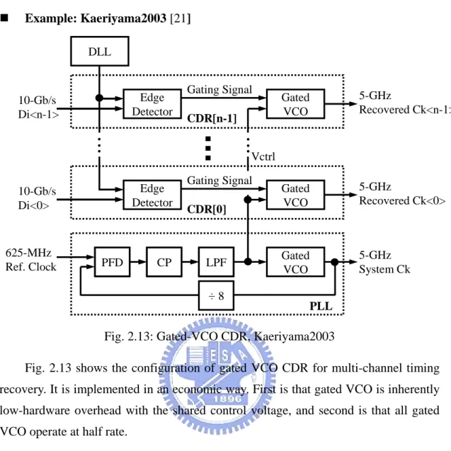
Example: Kaeriyama2003 [21] DLL Edge Detector Gated VCO Gating Signal CDR[n-1] Edge Detector Gated VCO Gating Signal CDR[0]
..
.
..
.
Gated VCO PFD CP LPF PFD CP LPF ÷ 8 5-GHz System Ck 10-Gb/s Di<0> 625-MHz Ref. Clock 5-GHz Recovered Ck<0> 5-GHz Recovered Ck<n-1> Vctrl PLL 10-Gb/s Di<n-1>Fig. 2.13: Gated-VCO CDR, Kaeriyama2003
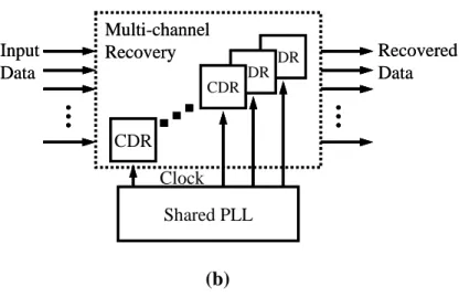
Fig. 2.13 shows the configuration of gated VCO CDR for multi-channel timing recovery. It is implemented in an economic way. First is that gated VCO is inherently low-hardware overhead with the shared control voltage, and second is that all gated VCO operate at half rate.
The CDR macrocell consists of 1) edge detector, 2) a gated VCO, 3) phase detector, and 4) reference voltage generator, where 3) and 4) are not shown in the figure.
The implementation is fabricated in 0.15-µm CMOS technology. Each CDR macrocell recovers 10-Gb/s data with a power dissipation of 50 mW at a 1.5-V supply, while area is 120 130 µm× 2. But the mentioned area excludes the hardware corresponding to data recovery such as the de-multiplexer for the half-rate data and the retiming circuit.
2.5 Alternative
&
Hybrid
This section introduces alternative CDR architectures, which involve a new recovering method, called FSM-based, and two hybrid architectures.
2.5.1 Alternative
CDR
FSM-Based, Analui2005 [22] Combinational Logic for States One-Bit Delay Output Logic Do<0> Do<1> Do<n-1> Di Previous State…
Fig. 2.14: FSM-based CDR, Analui2005 (a) Architecture (b) State Diagram at n=2 The FSM-based architecture is clockless and digital. Fig. 2.14(a) shows the CDR architecture with 1-to-n de-multiplexing, which includes two combinational logic circuits and the one-bit delay circuit. The one-bit delay is implemented with L-C delay cells. The recovered data output depends on the current input and the previous state from the delay line. It is therefore an asynchronous system but synchronized to every transition of incoming data.
The 1-to-n de-multiplexing relaxes the operation rate. Since the state information is kept in the memory of FSM and lasting for n-bit time. This system behaves like open-loop and operates without jitter rejection. The 1-to-n de-multiplexing behavior inherently introduces (1/n) of input jitter to the output.
The implementation operates at 7.5 Gb/s and is fabricated in SiGe technology. It is built with 1-to-2 de-multiplexing. From the data rate and technology, the digital-circuit approach still encounters speed limitation in timing recovery.
2.5.2 Hybrid
CDR
A hybrid version of oversampling/PLL architecture, called semi-blind, is proposed by Ierssel in 2006. Fig. 2.15 shows the architecture. The main system is a blind oversampling architecture, while the second feedback loop shown in the bottom of the figure simulates the PLL-based system. The second feedback loop is composed of a DAC and a loop filter. The original blind oversampling architecture tracks the
S1,0 S’0,1 S’0,0 S0,0 S0,1 S’1,0 S’1,1 S1,1 1 0 0 0 0 1 1 1 0 1 S1,0 S’0,1 S’0,0 S0,0 S0,1 S’1,0 S’1,1 S1,1 S1,0 S’0,1 S’0,0 S0,0 S0,1 S’1,0 S’1,1 S1,1 1 0 0 0 0 1 1 1 0 1 (a) (b)
high-frequency jitter while the second loop tracks the low-frequency jitter. The jitter tolerance specification at low frequency is greatly (32×) improved by this hybrid version.
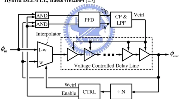
Fig. 2.16 shows a hybrid DLL/PLL CDR architecture by T. Lee. The data-deskew path forms the DLL, and the second loop in dashed line refers to the PLL. The system can be either a simple DLL-based CDR by removing the voltage controlled crystal oscillator (VCXO) path or a hybrid DLL/PLL system.
Both DLL and hybrid DLL/PLL architectures provide jitter-peaking-free timing recovery since no zero exists. In summary, DLL loop determines the acquisition speed while the filtering of low-frequency jitter benefits from the PLL loop.
The possibility of the hybrid DLL/PLL architecture can be further explored. Fig. 2.17 2 shows the weighted control of DLL and PLL by the interpolator. The original design in [26] uses a multiplexer to determine how the loop of the delay line is configured, open vs. closed. When the loop is closed, the delay cells forms an oscillator. In Fig. 2.17, the multiplexer is replaced by an interpolator, and through the weighted control, the behavior can be partial DLL and partial PLL. For instance, the hybrid ratio of DLL to PLL can be 50%-50%, 20%-80%, or anything else.
Semi-blind Oversampling CDR, Ierssel2006 [23]
20-phase 800-MHz VCO Samplers ×20 Di 8×4 FIFO Do Do wn Sam p le Decision Circuit DAC LPF 20-phase 800-MHz VCO Samplers ×20 Di 88×4 FIFO×4 FIFO DoDo Do wn Sam p le Decision Circuit DAC LPF
Fig. 2.15: Semi-blind oversampling CDR, Ierssel2006
2
Hybrid DLL/PLL CDR, T.Lee92 [24] Voltage Controlled Phase Shifter Di Phase Detector Loop Filter VCXO (External) Retiming Module Recovered Ck Recovered Do Clock In (for DLL mode)
Fig. 2.16: DLL & DLL/PLL CDR, T.Lee92
Hybrid DLL/PLL, Bae&Wei2004 [25]
Voltage Controlled Delay Line CP & LPF Up Dn Vctrl AND AND AND AND ÷ N in
φ
inφ
1-w w PFD Wctrl Enable outφ
CTRL InterpolatorFig. 2.17: Mixed PLL/DLL, Bae&Wei2004
2.6 Summary
Table 1 shows the summary on the CDR architectures, where ○ denotes yes, △
for partially yes, and X for no. As for the blank area, it is a currently un-explored field in this survey. Take the lack of digital implementation of Gated-VCO for example; fast analog circuits are required for the multi-gigabit timing recovery. And
even in today’s 10-Gb/s data rate in 0.13-µm CMOS technology, the analog circuits in [20] still employ passive inductors to overcome the bandwidth limitation.
Table 1: CDR architectures summary
Cont. Burst Analog Digital
PLL-Based ○ ○ △ Blind Oversampling ○ ○ △ ○ ○ a) Ck-Interpolation ○ ○ ○ ○ ○ b) Data-Deskew X ○ ○ ○ ○ Gated-VCO ○ ○ ○ Alternative FSM-Based ○ ○ & Oversampling/PLL ○ ○ △ △ Hybrid DLL/PLL ○ ○ ○ Multi-channel Application CDR Architectures DLL-Based
Operation Mode Implementation
This thesis adopts the data-deskew CDR architecture for 10-Gb/s/ch timing recovery, since a simple architecture is suitable for digital-circuit implementations. The chip is fabricated in 0.13-µm CMOS technology, and operates at a single 1.2-V supply.
Chapter 3
Deskew CDR:
System-Level Analysis
Design of the CDR follows a top-down design concept. The burst-mode multi-channel application introduces the system specifications as well as the architecture candidates. To implement with digital circuits, a DLL-based data-deskew CDR architecture is adopted. Once the architecture is determined, the details on system behavior can be figured out, and the design parameters can be derived.
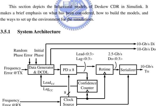
For “specifications-to-architecture” design, this section starts from the system architecture to provide a clear picture of the CDR. It is then followed by system specifications, design parameters, and the multi-channel synchronization behavior. Both behavioral and mathematical analyses are conducted. After that, the CDR is built and verified with the behavioral models in Simulink.
3.1 System
Architecture
The CDR targets at on-chip burst-mode timing recovery. It cooperates with an 8-phase PLL at the receiver site. Odd-phase clocks align to the edges of the input data.
They are recognized as the aligning clocks. Even-phase clocks are used as the sampling clocks. 10-Gb/s Di Control Codes 10-Gb/s Do Lead<0:3> Lag<0:3> 2.5-GHz P<0:7> CC Lead CC Lag Confidence Counter Confidence Counter Phase Control FSM Phase Control FSM P<0> PD × 8 Full-rate DCDL PD PD × 8× 8 Full-rate DCDL Loop Filter 2.5-Gb/s Do<0:3> Retime P<0> 2.5-Gb/s Do<0:3> Retime P<0>
Fig. 3.1: Deskew CDR system architecture
Fig. 3.1 shows Deskew CDR system architecture. It consists of 1) a full-rate DCDL, 2) phase detectors, 3) a confidence counter, 4) a finite state machine, and 5) the retiming stage.
DCDL adjusts the delay of the input data to obtain the optimal sampling phase. It aligns the mid-point of data period to the sampling clock. The full-rate circuit operation occurs only in DCDL. All circuits elsewhere operate in the quarter-rate domain.
Phase detectors are composed of eight flip-flops. They use the 8-phase quarter-rate clocks from PLL at RX. They are configured as 4 sets of Alexander phase detectors (APD), so 4 sets of Lead/Lag information are available from this block. The term Lead/Lag implies that the data leads/Lags the clock.
The digital low-pass loop filter is composed of a confidence counter and a phase control FSM. It emulates a single-pole R-C filter in continuous time domain but operates in discrete time domain instead. The closed loop bandwidth is determined by the counter size N.3
The confidence counter accumulates the 4 sets of Lead/Lag information. If the counting value exceeds the limitation of N/-N, the output LeadCC/ LagCC will be produced. FSM updates its state according to LeadCC/ LagCC from the confidence
3
The counter size N refers to the 10-Gb/s domain, even though the confidence counter operates in 2.5-GHz domain. For the case of N = 24, it implies that the minimum phase update time is 24-bit time or 2.4 ns.
counter. The current state of FSM determines the control codes of DCDL.
By adding or removing delay, the CDR will finally come to its lock state. In phase detectors, the data is recovered and inherently de-serialized into parallel data. Then, the retimed four 2.5-Gb/s data are available from this system.
3.2 System
Specifications
Table 2: Specifications of the 10-Gb/s Deskew CDR
Burst-data length 1200 bit
Frequency tolerance ± 500 ppm
Peak-to-peak clock jitter between TX and RX 0.4 UI
Tuning range of DCDL 1.4 UI
Phase resolution of DCDL 6 ps
DCDL-induced Jitter 0.1 UI
In Table 2, the length of the data packet is 1200-bit time. It includes a preamble of 176 bits for the initial clock recovery. The tuning range of DCDL is 1.4 UI, where the 1-UI delay is for compensating static phase offset and the 0.4-UI delay is for tracking the frequency error.
According to the frequency tolerance specification, the CDR is able to handle the frequency error of ±500 ppm. Or, the CDR can respond to the certain frequency error as long as DCDL does not overflow. In our definition, this is a dynamic specification to the CDR.
Since the data-deskew type CDR has a finite tuning range, the peak-to-peak clock jitter specification should be considered together with the frequency tolerance specification. The clock jitter specification confines the total accumulated phase error to 0.4 UI during each burst period. It guarantees that DCDL will not overflow.
3.3 Design
Parameters
3.3.1 Acquisition
Time
Acquisition time is the time to obtain optimal sampling phase. It is the initial tracking time of the CDR. To simplify the analysis, two assumptions have been made.
First, assume the frequency error between TX and RX is small enough and can be neglected. Second, assume that phase detectors give correct Lead/Lag information.
When the system is just initialized, the input data requires some delay to align to the sampling clock. For the best case, the delay is zero. It just aligns to the correct phase at the first place. As for the worst case, it requires the delay of half UI, or 50 ps. According to the fact of probability, the average required delay is ±25 ps or 25 ps in the absolute value. Fig. 3.2(a) shows the timing diagram of the average acquisition.
(a) (b)
Fig. 3.2: (a) Avg. required delay (25ps) (b)4-bit time transition probability
Assume the edge density d for one-bit time is 0.5. So, the transition probability for continuous 4-bit time is (1 - d4) = 15 16, shown in Fig. 3.2(b). The average acquisition time of this system is
25 ps Phase Update Time
Avg. Acquisition Time = .
Avg. Resolution×4-bit-time Transition Probability (3.1)
Consider the counter size N = 24, average phase resolution is 6 ps, and phase update time is N 1 UI = 2.4 ns× . By substituting them into (3.1), the average acquisition time is 10.67 ns, or 107-bit time. As for the worst acquisition time, it is double the previous value or 21.33 ns, or 213-bit time.
3.3.2 Loop-Latency
Constraint
The term loop latency sums up the circuit operation time through the whole loop. 1 2 1 2 1 2 1 2 Transition Probability 4-bit Time 10-Gb/s Di 4
Probability of at-least-one transition
1 15 = 1- 2 16 ⎛ ⎞ = ⎜ ⎟ ⎝ ⎠ P1 P0 P2 P4 P3 P5 P6 P7 10-Gb/s Do 25ps Init. Cond.
It is the total process time of the loop. The term loop-latency constraint is
Loop Latency < (N 1 UI).× (3.2)
where N is the counter size. The loop-latency constraint has to be considered for any closed-loop system. If this constraint is not met, the out-of-date Lead/Lag decisions will be accumulated in the loop. The unstable locking behavior may degrade the performance of the CDR or even cause oscillation.
3.3.3 Frequency
Tolerance
The frequency tolerance is the maximum frequency error between TX and RX that a CDR can deal with. The frequency tolerance depends on what noise profile is adopted. This analysis starts with an introduction to two types of noise profiles. The first one has the uniform distribution and the second one has Gaussian distribution, which represent the worst and the best cases respectively. [27]
PP
J
Aligning Clock
Fig. 3.3: Data eye diagram with the sampling clock
φ
P Lφ
Aligning Clockφ
P Lφ
Aligning Clock (a) (b)Fig. 3.4: Jitter models of a) the uniform distribution b) Gaussian distribution Consider the CDR operates at lock state. The aligning clock aligns to data edge with a phase error. Fig. 3.3 shows the data eye diagram with the aligning clock. In Fig. 3.4, the phase error is denoted as φL. It is the phase offset from the center of the jitter
distribution.
The probabilities of Lead/Lag are functions of φL. In this work, Lead and Lag control the Up and Down counting of the confidence counter.4 Their probabilities are denoted as P and P . u d
Fig. 3.4(a) shows the noise profile of the uniform distribution. The probability of Up in the gray area is
u / 2 P pp L. pp J J φ − = (3.3)
To derive the frequency tolerance, firstly discover the net probability of Lag to that of Lead. The net probability of Down to that of Up is
(
)
d u u u 2 P P 1 P P L. pp J φ − = − − = (3.4)Fig. 3.4(b) shows the noise profile of Gaussian distribution. The probabilities of this noise profile can be expressed as
u P L , rms Q J φ ⎛ ⎞ = ⎜ ⎟ ⎝ ⎠ (3.5) d u P P 1 2 L . rms Q J φ ⎛ ⎞ − = − ⋅ ⎜ ⎟ ⎝ ⎠ (3.6)
According to (3.4) and (3.6), frequency tolerances of the uniform and Gaussian distributions are derived in (3.7) and (3.8) respectively.
2 , L PP f d f N L J φ ⎛ ⎞ ∆ = ⎜ ⎟ ⋅ ⎝ ⎠ (3.7) 1 2 L . rms f d Q f N L J φ ⎛ ⎛ ⎞⎞ ∆ = ⋅ ⎜ − ⎜ ⎟⎟ ⎝ ⎠ ⎝ ⎠ (3.8)
where ∆ is the frequency offset. L is the number of steps per unit interval. The f
value of L is
Data Bit Time (1UI) 100 ps
~ 16.67.
Phase resolution 6 ps
L= = (3.9)
4
Lead/Lag indications result in Up/Down counting behaviors. They also refer to “adding delay to data/removing delay from data” in this work.
To simplify the simulation, certain assumptions have been made. 1) φL= phase resolution = 0.06 UI, 2) the equivalent edge density = 1−
( )
1/ 2 4= 15/16, and 3)= 0.4 UI PP
J , Jrms ≈0.04 UI. The simulation result of the frequency tolerance is
shown in Fig. 3.5.
(a) (b)
Fig. 3.5: Simulation of frequency tolerance (a) the main plot (b) a zoom-in version
3.3.4 Counter
Size
The frequency tolerance is a function of the counter size N. The larger N results in the narrower bandwidth. In this case, the high-frequency noise can be filtered out more but at the cost of slower response for the acquisition. On the contrary, the smaller N can handle a larger frequency error. It gives a faster response for the acquisition time.
To determine N, firstly consider the specification of the frequency tolerance. It is
± 500 ppm or 1000 ppm in the tolerant range. Assume a noise profile has both the
uniform and Gaussian distributions, and the ratio of the proportions is 50% to 50%. In Fig. 3.5(a), the maximum N for handling the 1000-ppm frequency error equals to 31. Since the confidence counter operates in 2.5-GHz domain, the loop filter updates its information every 4-bit time in 10-Gb/s domain. The candidates of N should be the multiples of 4, such as 28, 24, 20, etc.
The minimum N is introduced to the system by the loop-latency constraint. Even in the pseudo-NMOS circuit implementation, the process time of the entire loop
N=24 N=31
a b 1939 ppm
requires at least 6 cycles of the 2.5-GHz clock. The candidates of N are 24 or 28 now. To achieve faster acquisition, the smaller N is chosen.
In turn, the decision of N = 24 can derive an equivalent noise profile. From Fig. 3.5(b), the proportion of the uniform distribution to that of Gaussian distribution equals to ( a : b ), where a≈75%, b≈25%. The derived noise profile is stricter than the initial 50%-50% assumption.
In summary, the CDR is designed with a counter size N of 24. It is capable of the 1000-ppm frequency tolerance with a noise profile of 75% uniform and 25% Gaussian
distributions.
3.3.5 Loop
Bandwidth
The closed-loop bandwidth of the CDR can be approximated and measured by adding a simple sinusoidal jitter to the input [28]. The maximum slope of the sinusoidal input jitter is handled by the CDR. The slew rate of the CDR should be larger than the maximum slope of the sinusoidal input jitter below the loop bandwidth fBW.
The relationship between the frequency tolerance ∆f / f and the slope of the input jitter is (2 ), / . 2 j BW BW j f A f f f f f A π π ∆ = ⋅ ∆ = j
A is the jitter amplitude in second in (3.10), and fBW is inversely proportional to A . So the loop bandwidth decreases as the input jitter amplitude grows. j
Considering both the noise profiles of the uniform and Gaussian distributions and N = 24, we can derive the relationship of fBW and A from (3.7) - (3.10), shown in j
Table 3.
Table 3: The loop bandwidth fBW vs. the input jitter amplitudeA j
0.2 UI 0.3 UI 0.4 UI
22.4 MHz 10.0 MHz 5.6 MHz
37.2 MHz 23.5 MHz 15.4 MHz
Input jitter amlitude Aj
of uniform distribution BW f of Gaussian distribution BW f (3.10)
3.3.6
Delay Line Related
Tuning Range is the maximum tuning delay that DCDL can afford. Or, it is the difference between the maximum and the minimum data delay. In our system, it is 1.4 UI or 140 ps. The tuning range of 1.4 UI can be divided into two parts. In the worst case, the 1-UI delay is used to obtain the optimal sampling phase. And, the 0.4-UI delay is used to track the frequency error.
Phase Resolution is the minimum tuning delay. It is developed by advancing one LSB of the control code. The average phase resolution is the tuning range divided
by the number of codes. The specification for the average phase resolution is 6 ps. Input Sensitivity is the required minimum input amplitude that the input stage can handle and amplify to a target level. The specification is ± 50 mV.
3.3.7 Peak-to-Peak
Clock
Jitter between TX and RX
The peak-to-peak clock jitter specification is a constraint for both PLLs at TX and RX. During timing recovery, the total peak-to-peak clock jitter has to be confined. Even with the frequency error between TX and RX, the total accumulated phase error in each burst period must follow this specification. The allowed peak-to-peak jitter between TX and RX for the CDR is 0.4 UI.
An equivalent frequency error of 333.33 ppm can be derived from this 0.4-UI peak-to-peak jitter. To simplify the analysis, we assume the frequency error is a frequency step. This frequency step is applied to the CDR at lock state. The accumulated phase error ∆t in second can be represented as
(
)
-6 0 0 err -6 0 err -6 err 0 1 1 t = k , f f (1+f 10 ) 1 1 = k 1 , f 1+f 10 1 k f 10 . f ⎛ ⎞ ∆ ⋅ ⎜ − ⎟ ⋅ ⎝ ⎠ ⎛ ⎞ ⋅ ⎜ − ⎟ ⋅ ⎝ ⎠ ≈ ⋅ ⋅ ⋅where k denotes the bit length of data packet. The full-rate f equals to 10 GHz, and 0
err
f denotes the frequency error in ppm. Rewrite (3.11),
-4 err
t = k f 10 ps.
∆ ⋅ ⋅ (3.12)
Substitute t = 40 ps∆ , k = 1200 into (3.12). The equivalent frequency error of 333.33 ppm is derived.
3.4 Multi-Channel
Synchronization
50ps 50ps 0 1 2 3 4 5 6 7 Ch1 Delayed Do Ch1 Di Ch2 Di Ch2 Delayed Do P1 2.5-Ghz P0 P2 P4 P3 P5 P6 P7 0 1 2 3 4 5 6 7 0 1 2 3 4 5 6 7 0 1 2 3 4 5 6 7 Ch1 Init. Do Ch2 Init. Do 0 1 2 3 4 5 6 7 D0 D1 D2 D3 Recovered Ch1 D0 D1 D2 D3 Recovered Ch2 0 1 2 3 0 1 2 3 0 1 2 3 0 1 2 3 8 9 8 9 8 8 0 1 2 3 4 5 6 7 8 8 0 1 2 3 4 5 6 7 0 1 2 3 4 5 6 7 0 1 2 3 4 5 6 7 0 1 2 3 4 5 6 7 0 1 2 3 4 5 6 7 0 1 2 3 4 5 6 7 0 1 2 3 0 1 2 3 0 1 2 0 1 2 8 9 8 9 8 8 (a) (b)Fig. 3.6: Multi-channel data recovery (a) aligning case (b) shifting 1-bit case This section depicts the synchronization behavior of multi-channel timing recovery. The recovered data of multiple channels are synchronized to a particular clock phase of PLL. Ideally, the edges of the multi-channel data align to the same odd-phase clock. That is, the recovered first bit of the first channel aligns to the recovered first bit of the Nth channel. But for the practical usage, the edges of the multi-channel data may align to different odd-phase clocks of PLL. It depends on the skews among channels.
Fig. 3.6 illustrates a 2-channel timing recovery. The Init. Do is the initial output
to the data in the initial setting. After that, the data delay can be tuned by: 1) adding more delay to the data, or 2) removing the added delay from the data. Delayed Do
denotes the output data of DCDL when the system comes to its lock state.
In this work, even-phase clocks are the sampling clocks. The 4 recovered data D<0:3> are developed from P<0>, P<2>, P<4>, P<6> respectively. They are sampled by P<0> again. Assume the clock-to-Q delay is zero. The recovered data D<0:3> are derived after two clock period of P<0>.
Fig. 3.6(a) shows the delayed Do of Ch1 and that of Ch2 align to the same clock. So, the recovered data of Ch1 and that of Ch2 are aligned. In Fig. 3.6(b), the delayed Do of Ch1 and that of Ch2 are skewed by 1-bit period. So, the recovered data are shifted by 1-bit position. The parallel data re-arrangement is to be handled at a higher level.
3.5 Behavioral
Models
This section depicts the behavioral models of Deskew CDR in Simulink. It makes a brief emphasis on what has been considered, how to build the models, and the ways to set up the environment for the simulations.
3.5.1 System
Architecture
Serializer 10-Gb/sTo 2.5-Gb/s Do<0:3> Confidence Counter Confidence Counter Retime Lead<0:3> Lag<0:3> Data Generator & DCDL PD × 8 Frequency Error @TX Random Phase Error Initial Phase 8 CC Lead Frequency Error @RX Clock Source CC Lag 10-Gb/s Di 10-Gb/s DoFig. 3.7: Deskew CDR system architecture in Simulink
generates the full-rate PRBS data to DCDL. The initial phase of the input data of
DCDL is parameterized. And, the frequency error at TX is added here.
The frequency error at RX is added in the clock source. Besides, an additional
block Serializer is introduced to the system. It generates the 10-Gb/s output data To
for the comparison to Di and Do, where Di is the input data of DCDL, and Do is the output data of DCDL.
3.5.2
Data Generator & Delay Line
sin PRBS Generator Overflow Detector OverFlag sin PRBS Generator Di
Input Data Generator
Low-Pass Filter Do 1/S 1/S 10 GHz Frequency Error @TX Random Phase Error CC Lead CC Lag Initial Phase VAR φ
Fig. 3.8: Data generator & DCDL in Simulink
In Fig. 3.8, there are two signal paths, Di’s path and Do’s path. Di is the input of
DCDL. Do is the delayed and noisy output of DCDL.
For Di’s path, the 10-GHz frequency adds the Frequency Error at TX. Through
the integrator 1/S, the frequency is converted to a phase. A sinusoidal function,
denoted as the sin block, transfers this phase into a clock in time domain. The PRBS
generator uses this clock and generates Di with the frequency error of TX. The initial phase of Di is parameterized by Initial Phase. Note that Di is not actually fed to
DCDL in this configuration, but it does model the input data of DCDL.
For Do’s path, it begins from the input LeadCCand LagCC to the output Do. The tuning behavior of DCDL is modeled by adjusting the clock phase of the PRBS generator. It is based on the fact that Adding delay to data is equivalent to removing delay from the clock.
In the original design, DCDL adds one phase resolution to the data when
CC
resolution. So, in Fig. 3.8, the input LeadCCis together with a negative notation.
CC
Lag has the similar function as LeadCC. The phase is then added with a random phase error. Through sin block, the phase is converted to the clock. The following PRBS generator synchronizes to this clock. It generates a random pattern in the polynomial of (1+ +x3 x31). Finally, the data pattern goes to the Low-pass Filter
block, so the ISI effect is also modeled. The implementation of this block includes a low-pass transfer function and a hysteresis comparator.
Besides these two signal paths, there is a path for the overflow indication,
OverFlag. The tuning range specification of DCDL is 1.4 UI. OverFlag validates
when the accumulated tuning phase φVAR is above 0.7 UI or below -0.7 UI.
3.5.3 Noise
Sources
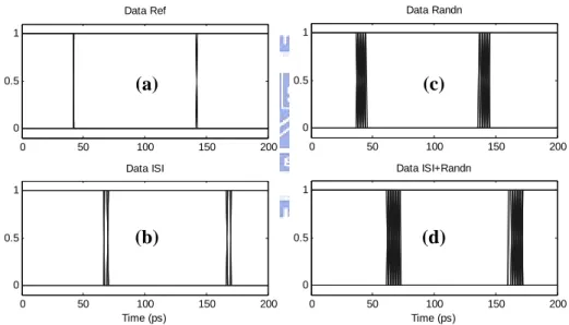
0 50 100 150 200 0 0.5 1 Data Ref 0 50 100 150 200 0 0.5 1 Data ISI Time (ps) 0 50 100 150 200 0 0.5 1 Data Randn 0 50 100 150 200 0 0.5 1 Data ISI+Randn Time (ps)Fig. 3.9: Adding noise sources in Simulink (a) a reference eye (b) ISI effect (c) random noise (d) the combination of ISI and random noise
To simply observe how the noise profiles affect the eye diagram, the path of
CC CC
(Lag -Lead ) in Fig. 3.8 is temporarily removed. Do is the output of DCDL in Fig. 3.8. Fig. 3.9 shows the eye diagrams of Do.
In Fig. 3.9, case (a) shows the ideal eye diagram of Do. In case (b), it shows the eye diagram with ISI effect. Comparing to case (a), the eye is delayed due to the low-pass transfer function. The deterministic jitter is added. In case (c), it shows Do with random phase noise. A ±4σ Gaussian model is applied. In case (d), it shows
(a)
(b)
(c)
the combination of both ISI and random phase noise.
For those eyes in Fig. 3.9 except the reference one, their jitter histogram plots are given in Fig. 3.10.
(a) (b) (c)
Fig. 3.10: Jitter histogram plots of (a) ISI (b) Random noise (c) ISI and Random noise
3.5.4 Phase
Detectors
Fig. 3.11 shows eight DFFs serving as the phase detectors. P<0:7> are the sampling clocks. The edge spacing for each adjacent clock is 50 ps. Every 3 DFFs and 3 XORs compose a set of APD. There are 4 sets of APD in this block. Therefore, ther are 4 sets of Lead/Lag outputs.
DFF DFF P0 DFF DFF P1 DFF DFF P2 DFF DFF P3 DFF DFF P4 DFF DFF P5 DFF DFF P6 DFF DFF P7 DFF DFF P0 DFF DFF P0 DFF DFF P0 DFF DFF P0 DFF DFF P0 Delay XOR XOR XOR XOR XOR XOR XOR XOR A A Lead<0> Lag<0> Lead<1> Lag<1> Lead<2> Lag<2> Lead<3> Lag<3> Lead<0> Lag<0> Lead<1> Lag<1> Lead<2> Lag<2> Lead<3> Lag<3> Di
Fig. 3.11: Phase detectors’ block in Simulink
In phase detectors’ block, Clock to Q Delay T is critical. All the even-phase CQ clocks align to the midpoint of the data period. They sample the intput Di at the optimal phase. So, T of even-phase detectors is 50 ps. The odd-phase clocks align CQ to the transition edges of the input Di. The T is degraded to 125 ps. Behaviors of CQ
the circuit-level T determine the retiming scheme for APD, and thus need special CQ
cares.
3.5.5 Confidence
Counter
The confidence counter and the phase control FSM compose the digital low-pass
filter. The filter contributes a pole to the CDR. But for the configuration shown in Fig. 3.7 and Fig. 3.8, the FSM is modeled by the integrator 1/S in DCDL. The tuning
phase of DCDL is derived instantaneously from LeadCC/ LagCC instead of the
control codes of FSM. So, there is not a specific block named FSM in Fig. 3.7.
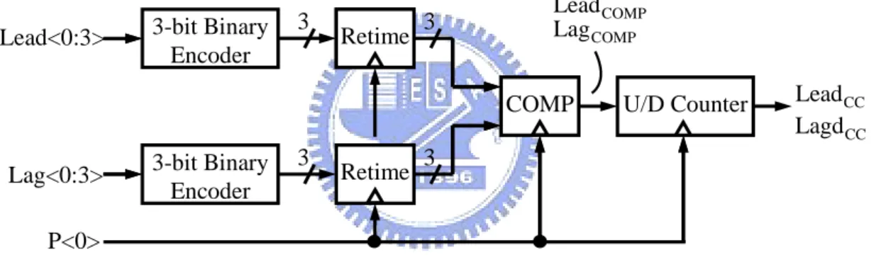
Lead<0:3> 3-bit Binary 3 RetimeRetime Encoder
Lag<0:3> 3-bit Binary 3 Retime Encoder
U/D Counter LeadCC CC Lagd COMP Lead COMP COMP P<0> COMP Lag 3 3
Fig. 3.12: Confidence Counter in Simulink
In Fig. 3.12, the count of Lead<0:3> is encoded into 3-bit unsigned integer, and so does that of Lag<0:3>. After retiming, the integers are compared in COMP block.
The comparison determines which integer is the larger one. LeadCOMPwill be true if the encoded integer from Lead<0:3> is the larger one.
The comparison result LeadCOMP/LagCOMP goes to the U/D Counter for further
accumulation. If the counting value reaches the maximum/minimum limitations,
CC CC
Lead / Lag will be validated. Then, the counter will be reset to its initial state immediately.
The comparator COMP introduces the majority-vote scheme. For the comparing cases of (4:0), (3:1), (3:0), (2:1), (2:0) or (1:0), they all regard the larger integer as 4. The counting limitations of the final counter are +6/-6, and the equivalent counting
values are +24/-24 respectively. The equivalent counting values refer to the whole confidence counter’s size N = 24 mentioned previously. The equivalent edge density is also enhanced by this scheme.
3.6 Behavioral
Simulations
This section gives demonstrations of the full-system simulation. Di is the
10-Gb/s input data of DCDL. Do is the delayed output data of DCDL. To is serialized
from the parallel recovered data for comparison. P<0> is the 2.5-GHz system clock.
3.6.1
Random Phase Noise
Fig. 3.13 gives an average case of the required 25-ps tuning delay, i.e., it requires
4 phase steps to obtain the optimal sampling phase. At the lock state, it shows how the Gaussian noise affects the locking behavior. In this simulation, ISI effect is intrinsic inside DCDL. The amplitude is 0.1 UI.
Fig. 3.13 (a) shows the case without Gaussian noise as the reference case. Fig. 3.13 (b) introduces 0.2-UI Gaussian noise. At lock state, the frequency of the Lead/Lag in (b) is lower than that in (a). It implies that the loop bandwidth is reduced. Fig. 3.13 (c) introduces 0.4-UI Gaussian noise. The system locks to another phase state, which is different from (a) and (b), due to the large random noise.
(a) Di Do To P<0> Time in 10 ns CC Lead CC Lag
(b)
(c)
Fig. 3.13: Simulations of random noise (a) free of random noise (b) 0.2-UI random noise (c) 0.4-UI random noise
3.6.2 Loop
Latency
To observe how the loop latency affects the systematic locking behavior. First, remove the noise sources from the system. So that, decisions of phase detectors are made from the precise data. Second, apply a periodic input to the CDR. Because, the maximum Lead/Lag decisions occur at the maximum edge density of the input data. These two conditions introduce the worst case that breaks the loop-latency constraint.
Fig. 3.14 shows the simulations of the loop latency in four cases (a) loop latency < (1N 1 UI)×
(b) (1N 1 UI) × ≤ loop latency < (2N 1 UI)× (c) (2N 1 UI) × ≤ loop latency < (3N 1 UI)× (d) (3N 1 UI) × ≤ loop latency < (4N 1 UI)×
For the ease of explanation, Lead and Lag is denoted as A and B. Case (a) is exactly the definition of the loop-latency constraint. The system locks at a continuous A-B-A-B state since the constraint is met. In case (b), the system locks at the A-A-B-B state when the latency is just over the constraint. The more latency will introduce the more instability to the system. As shown in case (c), it locks at the A-A-A-B-B-B state, and case (d) locks at the A-A-A-A-B-B-B-B state.
CC Lead CC Lag CC Lead CC Lag
It is obvious that an extra latency (N 1 UI)× introduces an extra repeating pattern (A-B) to the lock state. Because, the extra latency allows those out-of-date Lead/Lag decisions to be trapped and released in the loop later.
(a)
(b)
(c)
(d)
Fig. 3.14: Simulations of loop latency Di Do To P<0> Time in 10 ns CC Lead CC Lag CC Lead CC Lag CC Lead CC Lag CC Lead CC Lag