國 立 交 通 大 學
電子工程學系 電子研究所碩士班
碩 士 論 文
天線效應於0.13微米快閃記憶體所造成的損害及如何避
免和良率提升之研究
Study the Damage of Antenna Effect in 0.13μm
Flash and Yield Enhancement about
Reducing Antenna Effect
研究生 : 廖 學 鉦
指導教授: 張 國 明 博士
天線效應於0.13微米快閃記憶體所造成的損害及如何避
免和良率提升之研究
Study the Damage of Antenna Effect in 0.13μm Flash and
Yield Enhancement about Reducing Antenna Effect
學生:廖學鉦 Student:Hsuen-Cheng Liao 指導教授:張國明 博士 Advisor:Dr. Kow-Ming Chang
國 立 交 通 大 學
電子工程學系 電子研究所碩士班
碩 士 論 文
A Thesis
Submitted to Institute of Electronics
College of Electrical Engineering and Computer Science
National Chiao Tung University
In Partial Fulfillment of the Requirements
for the Degree of
Master of Science
In
Electronics Engineering
November 2005
Hsinchu, Taiwan, Republic of China
中華民國九十四年十一月
天線效應於0.13微米快閃記憶體所造成的損害及如何避
免和良率提升之研究
研究生:廖學鉦 指導教授:張國明 博士
國立交通大學
電子工程學系 電子研究所碩士班
摘 要
在本論文中,我們發現天線效應在0.13微米的快閃記憶體中造成嚴重的損害。 而天線效應的產生是因為在製的過程中有必須的電漿的乾蝕刻,以及金屬﹝鋁、銅 、鎢﹞的沉積。所以是無法避免的。若是天線效應發生時會對於元件造成如何的損 害呢?帶電的離子會由導電的金屬表面進入電路的內部,進一步的穿透閘極氧化層 ﹝Gate Oxide﹞,就會造成元件的損壞。而損壞的結果會造成臨界電壓﹝Threshold Voltage﹞漂移,以及閘極崩潰電壓﹝Gate Oxide Breakdown Voltage﹞下降。這些 的破壞會造成元件的工作異常,並且會有可靠度的問題元件會提早老化。所以對於 積體電路而言天線效應是一個重要的課題。隨著製程的進步,在現在超薄閘極氧化 層的世代中更是須要考量天線效應對於閘極氧化層的影響。的面積與極氧化層﹝Gate Oxide﹞之間的比例,若比值越小則受天線的影響就越小 。而電路的佈局﹝Circuit Layout﹞也是影響天線效應的另一因素。若是給予適當 的電路的佈局可以將電漿的電荷導向基板﹝Substrate﹞,而電荷將不會再經由閘極 穿過氧化層再經基板消失。 所以經由適當的天線比的選擇就能減低電荷存留在線路中及對於閘極氧化層的 損害。而良好的佈局則是更能進一步減低天線效應的影響。綜合以上二項的改進就 能有提高生產的良率及可靠度。
Study the Damage of Antenna Effect in 0.13μm Flash and
Yield Enhancement about Reducing Antenna Effect
Student:Hsuen-Cheng Liao Advisor:Kow-Ming Chang
Institute of Electronics
National Chiao Tung University
ABSTRACT
In this paper, antenna effect is seriously damage gate oxide in the 0.13um FLASH memory process. The antenna effect is a phenomenon of gate oxide degradation by charge buildup in plasma-based manufacturing processes. The plasma is necessary process in via, contact etching and Al, Cu, W film deposition. If the charges discharge form conductor (metal, via) to dielectric (gate oxide), what will happen in device? The charges will tunnel the gate oxide to substrate, and they will be hurt the device. It direct influences the threshold voltage (Vt) and breakdown voltage of gate oxide, and it also influences the yield and reliability. With process development, gate oxide thickness is
less and less. The antenna effect is an important issue in ultra thin gate oxide process. Low antenna ratio can decease the antenna effect, and antenna ratio is the ratio of metal area to divide diffusion area. So layout is an important issue in antenna effect. Antenna effect is a process of charges accumulation occurring on floating segments of incomplete interconnect network that are connected to transistor gate only. Accumulated charge may result in gate oxide failures that degrade yield and reliability. A good router can reduce the antenna effect damage and getting higher yield and reliability.
If we can reduce the antenna ratio, the antenna effect will be deceased. But reduce antenna ratio is difficult. Additional reducing antenna ratio, a good router also can decrease charge in metal and efficiently reduce antenna effect. In this way we will get high yield and reliability.
誌 謝
首先,感謝我的指導教授張國明老師,在這兩年中所給我熱心的指導與教 誨,使我在學術研究及待人處事上獲益匪淺。 其次,感謝UMC FA Lab提供研究的環境和設備以及技術人員熱心的協助,使我 的研究可以順利進行。而諸位口試委員的蒞臨指導與建議,在此亦一併表達謝意。 最後,要感謝我的父母與家人,有了他們的支持與鼓勵,讓我在無後顧之憂 的情況下讓我順利完成學業與論文。Contents
Abstract (in Chinese) ...3
Abstract (in English) ...…... 5
Acknowledgments (in Chinese)...7
Contents ...…...8
Table Captions ...…...10
Figure Captions...12
Chapter 1 Introduction
1.1 Flash Structure and Test Item in PMOSFET...141.2 Plasma Generate and Charging-Induced Damage ...14
1.3 Motivation ... ...16
2.4 References...…...…...16
Chapter 2 Experimental of PMOS Flash fabricate Process and Failure
Analysis
2.1 Introduction...192.2 The Fabrication Process of PMOSFETS Flash...19
2.3 Detail of Measurement and Fail Analysis Techniques ...23
2.3.1 Characteristics of I-V...24
2.3.2 Photo Emission Microscope analysis gate oxide damage location...25
2.3.3 SEM Top view analysis ...25
2.4 Summary ...26
2.4 References...…...…...27
Chapter 3 The Experiment of IMD Removes by Dry Etching and CMP
to Verify Antenna Effect Damage Gate Oxide
3.1 The Every Layer Antenna Ratio...283.2 Experiment Split Condition CMP and Dry Etch to Remove SiN ...29
3.3 Experiment of via1 loading effect ...30
3.4 Summary...31
3.5 References...31
Chapter 4 The New Layout for Reducing Antenna effect
4.1 Introduction...334.2 New Layout and Antenna Ratio...34
4.3 Result...35
4.4 Summary...35
4.5 References...36
Chapter 5 Conclusions and Future Works
5.1 Conclusions...37Table Captions
Chapter 2
Table.2-1 Antenna effect induce gate oxide breakdown wafer map, and the breakdown voltage distribution map (Dummy pattern).
Table.2-2 Antenna effect induce gate oxide breakdown wafer map, and the breakdown voltage distribution map (2T Real Cell pattern).
Table.2-3 SG Breakdown Voltage I-V Curve Table.2-4 CG Breakdown Voltage I-V Curve
Chapter 3
Table.3-1 The table is Antenna ratio of two patterns (real cell, dummy cell), the every layer antenna ratio.
Table.3-2 It is Antenna Ratio in M1 and M2 of different pattern. High antenna ratio is also high fail ratio. The AR of real cell is less then dummy cell, and dummy cell has high fail ratio.
Table.3-3 The table is the split condition of dry etching power and time. The CMP process is no any fail die.
Table.3-4 The gate oxide breakdown fail ratio is proportion to the number of via. Table.3-5 It is the split item of experiment and experiment result. The more VIA is the high fail ratio.
the original layout (31.25%).
Table.4-2 It is antenna ratio of new layout. It reduces the antenna ratio in M1 form 6154 to 783.
Figure Captions
Chapter 1
Fig.1-1 1 T Flash schematic cross-section, it includes 1 transistor and 2 poly-Si gate, floating gate and control gate.
Fig.1-2 2 T Flash schematic cross-section, it includes 2 transistors, one is select gate, and the other is control gate.
Fig.1-3 Program biasing condition. The electrons generated by high bias drain junction underneath the gate. Hot electrons generated by band-to-band tunneling are being extracted toward the floating gate while the hole toward the drain junction area.
Fig.1-4 The biasing conditions of ears. The electrons are extracted out of the floating gate into the channel area by Fowler-Nordheim tunneling.
Chapter 2
Fig.2-1 1T Dummy Cell Layout Fig.2-2 1T Real Cell Layout Fig.2-3 2T Dummy Cell Layout Fig.2-4 2T Real Cell Layout
Fig.2-5 Schematic tunneling. (a) Fowler-Nordheim tunneling is through gate oxide and energy release in gate oxide. (b) Less thickness gate oxide, Fowler-Nordheim tunneling is through gate oxide. (c) Direct tunneling, the gate oxide thickness is less then 4nm.
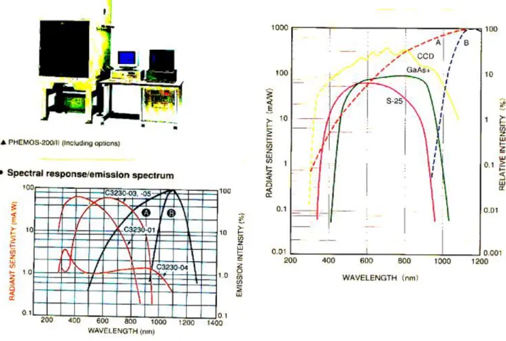
Fig.2-7 Photo Emission Machines Fig.2-8 EMMI System
Fig. 2-9 Photo Emission Spectrum, and CCD can detect spectrum area.
Fig.2-10 It is SEM Image. The mark place is the photoemission location. Intersect of poly-silicon gate and source line is emission place.
Fig.2-11 The hole of gate oxide is enhanced by KOH; it is SEM Top View Image Fig.2-12 Gate oxide was burn out by discharge; it is TEM Cross-section image. Fig.2-13 Gate Oxide Breakdown TEM Image
Fig.2-14 The breakdown gate oxide thickness is 6.8nm. It is the plasma damage place.
Fig.2-15 The gate oxide thickness is 7.4nm. It is in cell area.
Fig.2-16 The charge damage the gate oxide and leave dislocation on substrate surface; it is TEM Top View Image
Chapter 3
Fig.3-1 It is the split condition and the experiment process schematically.
Chapter 4
Fig.4-1 It is new layout. There is a new jumper with M1, via1 and M2. It connects all source line. It can reduce the antenna ratio in M1.
Fig.4-2 It is the P+ substrate and N Well band diagram. It is show greater band bending in P+ substrate when bias in gate (red line). It is the worst case for Plasma tunneling and damaged.
Chapter 1
Introduction
1.1 Flash Structure and Test Item in PMOSFET
The Flash is ETOX structure [1][2], it include 2 poly-silicon layers. And it includes two structures, one is one PMOS transistor and the other is two PMOS transistor. The top poly-silicon layer is control gate and the bottom poly-silicon layer is floating gate (Fig.1-1). There are two pattern of flash memory. One is 1T (Fig.1-1) structure; the other is 2T(Fig.1-2) structure. The program condition is that the electrons generated by high bias in the drain junction underneath the gate. Hot electrons generated by Band-to-Band Tunneling [3] are being extracted toward floating gate while the holes toward drain junction area (Fig.1-3). The erase condition is that electrons extracted out of floating gate into channel area by Channel-Fowler-Nordheim Tunneling [4] (Fig.1-4). Test item is measurement leakage between floating gate with channel (substrate). And the other test item is the measurement of leakage between floating with floating. The gate oxide thickness is 8.0nm. If the antenna effect damage gate oxide, gate oxide will be degrade and breakdown voltage decreased. We can find the leakage current between floating gates and substrate.
1.2
Plasma Generate and Charge Induce Damage
(>1E12/cm3)[5], and it is necessary in manufacturing of Ultra-large-scale-integrated (ULSI) circuits for the etching and deposition of films. The plasma process improves uniformity and line width control [6,7]. The ion energy is control by substrate bias and can be varied by changing plasma parameters. The advantages are product of completely ionized plasma at low pressure using radio-frequency (RF) waves, and expansion of the plasma uniformly to large diameter.
There are three types of plasma-based manufacturing process [8]: (1) Conductor layer pattern etching process.
Etching processes divide conductor layer plates into routing patterns. The amount of accumulated charge in the processes is proportional to the plasma-exposed area, which is proportional to the perimeter length of conductor layer patterns.
(2) Ashing processes.
Ashing processes [9][10] remove remaining photo resist layer after etching processes. The area of conductor layer patterns is directly exposed by plasma and the charge, whose amount is proportional to area of conductor layer patterns, is accumulated. (3) Contact etching processes.
Contact etching processes dig holes between two conductor layers. In the late stage of the processes, the area of all the contacts on the lower conductor layer pattern is directly exposed and the amount of accumulated charge is proportional to the total area of the contacts.
Antenna charging damage to thin gate oxide has been observed in almost every kind of plasma process and has become a major reliability issue [11]. The charge source is from plasma, and the way of damage gate oxide is Fowler-Nordheim (F-N) tunneling
(Fig.1-4). The F-N tunneling is known to result in the generation of interface traps and gate oxide trap. The more large metal area the more charge accumulated produces high electric field in gate oxide, and the charge will tunnel gate oxide or trap in it [12]. It degrades gate oxide. The threshold voltage (Vt) of MOSFET will be shift and gate oxide breakdown voltage also is decease. It is a serious influence issue in yield and reliability. If the plasma is no uniformity [13], the distribution is imbalance between ion and electron current density on the wafer surface. The local charges produce local current to balance the no uniform plasma potential. And the current will damage gate oxide. As long as any kind of no uniformity exists, the device quality will degrade [14].
1.3 Motive
For improving yield and reliability, we need to do some action about antenna effect. First, we to find out where are most weak point in device and layout. To verify the weak point is the location that antenna effect damages it or not. If we have make sure the failure place, we can use changing layout to do good router reduced charge tunneling gate oxide. The product is 0.13um flash memory; the most important issue is data retention time. The necessary condition to have long data retention time is good quality oxide. Improve the oxide quality; the yield and reliability improve, too.
1.7 References
[1] Wett, T.; Levy, S., “Flash-the Memory technology of future that’s here today,” IEEE Aerospace and Electronics Conference, vol. 22-26, Page(s): 359 - 364, 1995.
[2] Atwood, G, “Future directions and challenges for ETox flash memory scaling”, IEEE Transactions on Volume 4, Issue 3, Sept. 2004 Page(s): 301 - 305
[3] Takeda, E.; Matsuoka, H.; Igura, Y.; Asai, S.; ” A band to band tunneling MOS device (B T-MOSFET)-a kind of `Si quantum device'2 ”, Technical Digest, International
11-14 Dec. 1988 Page(s): 402 - 405.
[4] Suhail, M.; Harp, T.; Bridwell, J.; Kuhn, P.J, “Effects of Fowler Nordheim tunneling stress vs. Channel Hot Electron stress on data retention characteristics of floating gate non-volatile memories”, J Reliability Physics Symposium Proceedings, 2002. 40th Annual 7-11 April 2002 Page(s):439 - 440.
[5] C Charles, R.W. Boswell, A. Bouchoule,C. Laure, and P. Ranson, “Plasma diffusion from a low pressure radio frequency source,” J.Vac. Sci. Technol. A, Vol. 9(3),
P.661-663, may/Jun 1991.
[6] A.J. Perry,D.Vendoer, and R.W Boswell, “The application of helicon source to plasma processing,”, J.Vac. Sci. Technol. B, Vol 9(2), p.310-316, Mare/Apr 1991
[7] Nobuhiro Jiwari, Takayuki Fukasawa, and Hiroshi Kawakami, “Helicon wave [lasma reactor employing single-loop antenna”, J.appl. Phys., 72(10), p.4865-4872. 15
November 1992.
[8] H. hin, C.C.King, C. Hu, “ Thin Oxide Damage by plasma etching and ashing process”, J. Proc. Of IRPS, 1992.
[9] H. C. Lin, C. H. Chien, M. F. Wang, T. Y. Huang, and C. Y. Chang, “A model for photoresist-induced charging damage in ultra thin gate” in Int. symp. Plasma process-induced Damage (P2ID), 1997,pp.247-250.
Breakdown from Gate Charging During Resist Ashing,” IEEE Trans. Electron Devices, Vol. 41, No. 10, p, 1848-1853, October 1994.
[11] Sychyi Fang; McVittie, J.P.; “Oxide damage from plasma charging: breakdown mechanism and oxide quality”,IEEE Trans. Electron Dev., Volume 41, Issue 6, June 1994 Page(s):1034 - 1039
[12] Sung-Hyung Park; Hi-Deok Lee; Key-Min Lee; Myoung-Jun Jang; Joo-Hyoung Lee; Geun-Suk Park; Ki-Seok Yoon; Jung-Hoon Choi; Young-Jin Park; Hee-Goo Youn;” Dependence of plasma process induced damage on the transistor gate area”, 2001 6th International Symposium on
13-15 May 2001 Page(s):124 - 127
[13] Sychi Fang, Shigemi Murakawa, and James P. Mctti,”A New model for Thin Oxide Degradation from Wafer Charging in Plasma Etching,”IEDM Tech. Dig. P.61-64, 1992. [14] Sychyi Fang and James P. McVitti, “ A Mechanism for Gate Oxide damage in Non-uniform Plasma,” Proc. Of IEEE IRPS, p.13-17, 1993.
Chapter 2
Experimental of PMOS Flash Fabrication Process and Failure
Analysis
2.1 Introduction
In this chapter, the preparation of samples for PMOS Flash memory [1] and the failure analysis technique including apparatus is introduced. There four test-key pattern in the wafer. Because it includes two kind circuits, one is 1T(one transistor per bit) and 2T (two transistor per bit). Every circuit includes two pattern, one dummy cell and real cell. They layout is as figure. 1T dummy cell layout is Fig.2-1, 1T real cell layout is Fig.2-2, 2T dummy cell is Fig.2-3, and 2T real cell layout is Fig.2-4. First, it is fabrication process for PMOS Flash. The next, electronic failure analysis and physic failure analysis are introduced.
2.2 The Fabrication Process of PMOS Flash
The sample used to study characteristics of PMOS Flash is fabricated on 200mm, <100> oriented Si wafer. Fig.1-1 shows the schematically cross-section view of PMOS Flash. And the major process sequence is divided to two parts. Front end is STI formations, well formation, gate oxide and poly-gate; back end is via and Metal deposition. The detail process steps are listed as follows:
(1) Wafer start:
2.Lot ID laser mark. (2) STI formation:
1. Pad SiO2 deposition 11nm.
2. Pad SiN deposition 1200 3. Photo STI define 4. STI Etch
5. Deposition liner SiO2 15nm.
6. HDP STI SiO2 deposition 600nm.
7. STI CMP. (3) Alignment Mark 1. Photo alignment 2. Etch (3) Well formation 1. RCA clean 300s. 2. N well photo define 3. N well implantation:
a. Phosphorus, Dose: 6E13 cm-2, Energy: 600Kev. b. Phosphorus, Dose: 3E12 cm-2, Energy: 600Kev. c. Arsenic, Dose: 7 E11 cm-2, Energy: 400Kev. 4. PR strip
5. P well photo define 6. P well implantation:
b. Boron, Dose: 4E13 cm-2, Energy: 225Kev. c. Boron, Dose: 2E12 cm-2, Energy: 130Kev. 7. PR strip.
8. RTP well anneal (4) Gate Oxide fabrication
1. Standard RCA clean.
2. Gate oxide grown 8.0nm by N2O.
(5) Poly-Si Gate
1. P1 Poly-Si deposition 80nm. 2. Floating gate photo define. 3. Floating gate etching. 4. LPTEOS deposition 5.0nm 5. SiN deposition 4.0nm 6. LPTEOS deposition 5.0nm. 7. Define P2 pattern.
8. P2 etch.
9. Spacer deposition (TEOS 30nm,SiN 10nm) and etch. (6) Source/ Drain implantation
1. N+ implantation: a. N+ define
b. Phosphorus, Dose: 3E13 cm-2, Energy: 50Kev. c. Arsenic, Dose: 2.5 E15 cm-2, Energy: 40Kev. d. PR strip.
2. P+ implantation a. P+ define
b. BF, Dose: 5E14 cm-2, Energy: 15Kev. c. Boron, Dose: 3E15 cm-2, Energy: 4Kev. d. PR strip. 3. RTP anneals 1090°C. (7) Co-silicide formation 1. Deposition Co 11.0nm 2. RPT1 540°C 30s 3. Co etches. 4. RTP2 750°C 30s. (7) ILD fabrication
1. Deposition PECVD SiN 38.0nm
2. Deposition APCVD USG (SiO2) 200nm
3. Deposition PECVD TEOS PSG (SiO2) 800nm
4. CMP
5. Photo contact pattern define 6. Contact dry etch
7. Ti/TiN deposition. 8. W-CVD 300nm 9. W-CMP. (8) Metal1 fabrication
2. Deposition PECVD FSG 350nm 3. Deposition PECVD SiON 90nm. 4. M1 trenches Photo define. 5. M1 trench dry etch.
6. Cu ECP deposition 700nm. 7. Cu CMP.
(9) Via1 and Metal 2 fabrication 1. Deposition PECVD SiN 70nm 2. Deposition PECVD FSG 320nm 3. Deposition PECVD SiON 40nm. 4. Deposition PECVD FSG 350nm. 5. Deposition PECVD SiON 90nm. 6. Via1 Photo defines.
7. Via1 dry etch.
8. M2 pattern photo define. 9. M2 trench dry etch.
10. Cu ECP deposition 1000nm. 11. Cu CMP.
2.3 Detail of Measurement and Fail Analysis Techniques
The flash memory is operation in high voltage, so the test item also in high voltage (10V) and leakage current spec is less than 100nA. The flash test item of gate oxide breakdown almost all fail in 2 transistors pattern, but the 1 transistor pattern all pass. It
must something happen in the 2 transistors pattern. The mechanism of gate oxide leakage is Fowler-Nordheim tunneling and direct tunneling (Fig.2-5).
GOX>4nm the major tunneling is Fowler-Nordheim tunneling JFN=AEOX2exp[-BψB2/EOX]
JFN: Tunneling current density A, B: constant
EOX: oxide field ψB:: barrier height (~3.2eV)
GOX<4nm the major tunneling is Direct Tunneling
JDT= exp } ] / ) [( 1 { 1/2 2 2 B OX B OX qV AE φ φ − − 3/2 2 / 3 2 / 3 ] ) ( [ B OX OX B B E qV B φ φ φ − − − (2.1) JDT: Direct Tunneling current density
The Gate oxide is 8.0nm. It is major Fowler-Nordheim tunneling, and the electrons are accelerated by electron field (EOX) and collide the lattice. In colliding, the energy of
electrons broke the bond of atoms. The holes or electrons were trapped in GOX.
The wafer map of 2T dummy cell testing result is Table.2-1. It is almost fail. 2T real cell testing result is as Table.2-2. It is only 1 die fail. Test condition and spec: Vg=10V, Ig<100nA.
2.3.1Characteristics of I-V
The measurement of GOX current I-V curve is Table.2-3. It is compare 2transistor pattern with 1 transistor pattern. 1transistor pattern is all pass, but 2transistors pattern is almost all fail. The 2-transistor pattern leakage current is very large when Vg is higher then 8V, but the 1 transistor pattern is no leakage current when Vg is 10V.
2.3.2 Photo Emission Microscope Analysis Gate Oxide Damage Location
In I-V curve measurement, we just find the leakage current in gate oxide, but we don’t known what happen in device. We use the photoemission microscope (PEM) to detect the leakage current location. The mechanism is the electrons tunneling the gate oxide and recombine with hole (Fig.2-7). The instrument of PEM [2] is Fig.2-8. And the CCD detect emission spectrum area is as Fig.2-9. Emission spectrum is as equation 2.2.The recombination emit photo, and CCD can catch the emission. In this way, we can observe the failure location. The gate voltage that we input is 8V. We find out the emission hot spot as Fig.2-6, and find the emission spot always in the same location. By the way, it is a weak point in the circuit. After the EFA, we need to do physical fail analysis to find out the root cause of the failure.Emission spectrum g E 6 10 24 . 1 × − = λ m-eV (2.2)
λ : m Eg: Energy gap (Si:1.12eV)
2.3.3 SEM Top View Analysis
1. SEM sample preparation:a. M1 and M2 strip: CMP remove. b. ILD Strip: BOE 120s.
c. Poly-Si strip: KOH 80∘C 15s. 2. SEM Observation.
a. ILD remove (Fig.2-10).
2.3.4 TEM Cross-Section Analysis
1. TEM sample preparation:a. FIB trim sample to thickness 500nm. 2. TEM Observation:
a. Oxide breakdown image (Fig.2-12)(Fig.2-13). Oxide thickness 6.8nm (Fig.2-14).
b. Cell gate oxide 7.4nm, spec 8.0nm (Fig.2-15).
2.3.5 TEM Top view Analysis
3. TEM sample preparation:a. All layers strip by HF 300s. b. Back site substrate CMP. 4. TEM Observation:
a. Gate oxide breakdown induce substrate dislocation (Fig.2-16).
2.3 Summery
The gate oxide location was found in PEM. The spot is in peripheral circuit; it is always in intersect of poly-Si gate and source line not in cell area. The breakdown area is P+ area, which is different with cell area (N well). The hole on gate oxide was observed in SEM image and TEM image. We can easily find the hole always in the same place. It is must the worst place in the pattern.
[1] Seki, K.; Kume, H.; Ohji, Y.; Kobayashi, T.; “An 80-ns 1-Mb flash memory with on-chip erase/erase-verify controller” Solid-State Circuits, IEEE Journal of
Volume 25, Issue 5, Oct. 1990 Page(s):1147 - 1152
[2] Salome, P.; Leroux, C.; Chante, J.P.; Crevel, P.; Reimbold, G.;“Study of a 3D
phenomenon during ESD stresses in deep submicron CMOS technologies using photon emission tool”IEEE.Reliability Physics Symposium, 8-10 April 1997 Page(s):325 - 332
Chapter 3
The Experiment of IMD Removes by Dry Etching and CMP to
Verify Antenna Effect Damage Gate Oxide
In the chapter, we want to verify the gate oxide was damaged by antenna effect. When complete M2 process, gate oxide leakage current always was found in 2T dummy cell pattern. Two experiments were done to verify how does damage gate oxide by plasma of dry etching process? First, what condition will damage gate oxide in SiN strip by dry etch and CMP? Second, what is the relation gate oxide damage with via number that was expose in plasma?
3.1 The Every Layer Antenna Ratio (AR)
Antenna Ratio (AR) is an important parameter in VLSI process. Larger AR is more easily damaged by plasma [1]. For a fully exposed gate electrode, the collected current is proportional to the antenna electrode area, Af. The collected plasma current (Is) to the
gate is given by where we have changed to current by adding the device collection area, Af, which for an bare antenna structure is Af + Ag or just Af for Af >>Ag. Where Af is the
area of the conductor exposed to plasma, and Ag is the area of gate oxide. AR=Af/Ag. Je
is electron and Ji is the positive ion in plasma.
) ( i e c s A J J I = − (3.1) g FN f e i J A J A J − ) = ( (3.2)
And then (Ji − )Je AR= JFN (3.3)
We list every layer AR (antenna ratio) in the table.3-1. There are two patterns in table.3-1. Every layer AR of dummy cell is large then real cell. The WAT test result is dummy cell worst then real cell. (table.3-2). Test condition is gate voltage 10V, current is less then 100nA.The antenna effect induce gate oxide damage is relation with antenna ratio.
Dummy cell: large AR, fail ratio=68.75% Real cell: small AR, fail ratio=6.25%
3.2 Experiment IMD Remove by CMP and Dry Etch in Different Power
and time Process split
3.2.1 Experiment of IMD1 Remove, schematic in Fig.3-1: Experiment process Splits
(a). Deposition 70nm SiN on metal 1. CMP remove 70nm SiN.
(b). Deposition 70nm SiN. Photo define pad.
Dry etch in different Power and time (Table.3-3). Power: 500, 150 W.
Time: 35, 50, 60 s. 3.2.2 Result and discussion:
Sample (a) is no leakage current (Ig<100nA, Vg=10V), but the samples (b) are all failure (Ig>100nA, Vg=10V). No matter any condition of samples (b) leakage current are
all lager then spec100nA in 10V. The raw samples are finish M1 fabrication, and they are no leakage. But we can easily find out different result of experiment split. Split (a) is no plasma process, but samples (b) are all plasma process. The result in Table.3-3 is comparable. No plasma process (CMP) [3] is all pass, but plasma-base process is in different fail ratio. We easily find out the root cause of leakage current in gate oxide is plasma damaged.
3.3 Experiment of via1 loading effect
In last experiment, we find the root cause of damage gate oxide is plasma from dry etch. If we decrease the plasma of etch process, it can reduce the gate oxide damage. In the experiment, it decrease via1 number to reduce the plasma that pass M1 to gate oxide from via1 etching.
3.3.1 Experiment split condition: a. 0.5% via 1 number. b. 1.6% via1 number. c. 3.4% via2 number. d. 100% via1 number. The layout is as table.3-4
The final process is finish M2 fabrication.
3.3.2 Result and discussion:
The experiment split condition is as table.3-4, and wafer map is as table.3-5. The less via number (0.5%, 1.6%, 3.4%) are low fail ratio; the fail ratios are all less then 11%.
The 100% via1 is still high fail ratio; fail ratio is 70%. The gate oxide damage is proportional to via1 number. Via number is antenna electrode area (Af). In equation 2.1,
plasma current is proportion to antenna electrode area (Af)[4]. Although, decreasing via1
number can reduce fail ratio, but it cannot completely stop plasma damaged oxide.
3.4 Summary
In the chapter, we want to verify the gate damage root cause. It is plasma from dry etch. The antenna ratio is high relationship with antenna effect, and it is seriously impact gate oxide quality. When finish the circuit layout, the antenna ratio is not easy to change. So we need to find out other ways that can reduce antenna damage. The CMP is one kind of solutions. But CMP cannot whole replace dry etch. In this process, we need dry etching to etch trench of via and metal lines [5].
The second experiment is decreased via1 number, and it also can reduce gate oxide damage. But it cannot stop plasma damaged gate oxide. The decrease via1 number just can verify antenna ratio is proportion to fail ratio. It cannot use in our productions. Less via number will induce high resistance in circuit. We need to find out other solution of stop gate oxide damage.
3.5 References
[1] Maly, W.; Ouyang, C.; Ghosh, S.; Maturi, S.; “Detection of an antenna effect in VLSI designs” 1996 IEEE International Symposium on 6-8 Nov. 1996 Page(s):86 - 94
[2] Simon, P.; Luchies, J.M.; Maly, W.; “Identification of plasma-induced damage conditions in VLSI designs ” IEEE Tran. onVol. 13, Issue 2, May 2000 Page(s):136 –
144.
[3] Lin, S.; Changming Jin; Lui, L.; Minghsing Tsai; “Low-k dielectrics characterization for damascene integration” IEEE 2001 International4-6 June 2001 Page(s):146 - 148 [4] Simon, P.; Luchies, J.-M.; Maly, W.; “Antenna ratio definition for VLSI circuits [plasma etch damage]” 1999 4th International Symposium on9-11 May 1999 Page(s):16 - 20
[5] Watanabe, H.; Komori, J.; Higashitani, K.; Sekine, M.; “A wafer level monitoring method for plasma-charging damage using antenna PMOSFET test structure” IEEE Transactions onVolume 10, Issue 2, May 1997 Page(s):228 - 232
Chapter 4
The New Layout for Reducing Antenna effect
4.1 Introduction
In chapter 3, we realize the killer of gate oxide is plasma. But cannot stop it damage gate oxide. In chapter 2, we find out the gate oxide damage location, and it is on source line diffusion. No matter what dies fail, gate oxide damage location is always in the same place. It is an obviously hint, it is the most weak point on gate oxide. The largest F-N tunneling current is in the place. If a new layout is no the place, and new router will be avoid antenna effect damage. The original layout is source line (P+ diffusion) that crosses with poly-si gate. So we need to make a new mask that source line doesn’t cross over poly-Si gate.
In order to reduce or prevent damage to gate oxide from plasma-based process, and to ensure reliability, a circuit layout rule that considers the antenna effect is employed [1]. The conventional antenna rule restricts a maximum antenna ratio allowed for circuit layout. Recent studies show that the damage increases in proportion to both the area and the perimeter of the antenna. Consequently, the damage induced to the gate oxide terminal Ti can be calculated as follow:
) ( ) ( ) (Ti AR Ti PR Ti D = +
∑
× × +∑
× × = j j ij j j ij i j x P P P T P x A P A T A ) ) ( ) ( ) ( ( ) ) ( ) ( ) ( (α β (4-1)antenna perimeter length ratio of Ti, j∈{poly layer, all the via layer, and all the metal layers}, is a set of j-layer wires, A(x) is the area of pattern x which gate terminals connecting , P(x) is the perimeter length of pattern x, is constant is constant. Using the function, it is proposed that the objective function to be minimized during placement and routing the following form:
Pij ij P αj βj
∑
− Ti i D T D f Minimize ( ( ) max) (4-2) Dmax is the maximum allowable gate-damage value [2][3].4.2 New Layout and Antenna Ratio
The original layout is as Fig.2-3, source lines (P+ diffusion) connect together by P+ diffusion, and they are like fork. So the poly-si gate crosses with P+ diffusion (source line). The new layout (Fig.4.1) is new router in M1 [4]. Every source line is isolation in P+ diffusion, and they are connected by M2. In this way, it can avoid the poly-silicon cross with P+ diffusion, and make the worst point disappear in the new pattern. The weak point is like a capacitor structure, which is including top plane (poly-silicon gate), bottom plane (P+ diffusion) and dielectric (SiO2). And it is easily trap charges in plasma-base process. If the plasma is no uniform, the ions and electrons could be trap in top plane and bottom plane. It will be develop a high electron field in dielectric (SiO2) by the ions and electrons. When the charges discharge to substrate (P+ diffusion), the energy of charge damage the bond of silicone and oxygen (O=Si=O). And Gate oxide thickness of P+ diffusion area is less then cell area (N diffusion=80nm). So it more worst in the place. If we replace the pattern by new layout, the gate oxide damage problem could be
disappeared.
4.3 Results and Discussion
Test condition 1:VG=10V Ig <100nA
New layout pass ratio: 100%
Original layout pass ratio: 31.25% (Table.5.1) Test condition 2:
Ig=100nA to get VG.
New layout has higher breakdown voltage then original layout. The test result is as table.5.1. The result clear display the advantage of new layout, it improves the gate oxide breakdown voltage. It is 100% pass in the testing. The new layout new router is not only disappear the weak point, the antenna ratio also reduce in M1 (Table.5-2). In this way, we can guaranty gate high yield in WAT test. And what is the fail and pass mechanism. Fig.4-2 is the band diagram of P+ substrate and N well. When bias is input in gate, the greater band bending in A but B is smoother. The electron A will easily produce Fowler-Nordheim tunneling, but B is too high barrier of gate oxide to tunneling. We always find the gate oxide damage position is in A.
4.3 Summary
In the chapter, we do a experiment of modify layout. The original source lines (P+ diffusion) are all together, like a fork. All source lines are isolation, and router is contacts,
M1, via1 and M2 to connect all source line together. The new layout cancels the position A. The original worst place disappears, and there is no parasitism capacitor that will induce worst Fowler Nordheim tunneling between source line and poly-silicone gate. There is less leakage current in gate oxide, and it gates higher gate oxide breakdown voltage. And it need not change any process recipe. When it is finish all process until M8, the final test also show that is no any fail die. The new layout has completely solved the important problem antenna effect and damage gate oxide in plasma-base process.
4.4 References
[1] Tsung-Yi Ho; Yao-Wen Chang; Sao-Jie Chen;“Multilevel routing with jumper insertion for antenna avoidance” IEEE International12-15 Sept. 2004 Page(s):63 - 66 [2] h. Shin, C. C. King, C.Hu, “Thin Oxide Damage by plasma etching and ashing process,” Proc. Of IrPS, 1992.
[3] Watanabe, H.; Komori, J.; Higashitani, K.; Sekine, M.; “A wafer level monitoring method for plasma-charging damage using antenna PMOSFET test structure” IEEE Transactions onVolume 10, Issue 2, May 1997 Page(s):228 - 232
[4] K. P. wang, M. Marek-Sadowska, W. maly, “Layout design for yield and reliability,” 5th ACM SIGDA Physical Design Worshop, 1996.
[5] Krishnan, A.T.; Krishnan, S.; Nicollian, P.; “Impact of gate area on plasma charging damage: the "reverse" antenna effect” 2002. IEDM '02. Digest. International
Chapter 5
Conclusions and Future Works
5.1 Conclusions
In this thesis, three solutions of plasma damages gate oxide was propose and fabricated. Using failure analysis instruments find out the plasma damage gate oxide mechanism and special failure pattern. It is clearly display gate oxide pinhole in cross-section TEM image and top view TEM image. The gate oxide breakdown always begins in finishing M2 fabrication. The charges accumulate in M1, via1 and M2 process, and discharge to diffusion, charges energy damage gate oxide.
Three experiments are proposed to solve the gate oxide damage problem. (1) Using CMP process displace plasma-base process. It can completely reduce plasma, and no gate oxide damage. But the plasma-base etching is necessary in deep sub-micro VLSI; it must etch the trench in IMD for deposition Cu. It just verifies the damage is from plasma-base etching process. (2) It is via1loading effect experiment. Via1 connect M1, the plasma path is from via1, M1, poly-Si gate then tunneling gate oxide. Via number on probing pad is proportion to ion and electron number. The gate oxide damaged is also proportion to via number. But the less via number will increase resistance, high resistance induce long time delay. So less via cannot use in production. (3) It new router layout. The original source lines are all together by P+ diffusion, new layout P+ diffusion is displacing by the path that includes contact, M1 and M2. And the new layout is no the gate oxide damaged place which was found in FA. The new layout completely stops the plasma damaging
gate oxide. All sample 100% pass in the gate breakdown testing. The new router is no other side effect, and antenna ratio is decrease in M1. All sample passes in the final process M8 finish.
5.2 Future works
Now, we realize where is the worst place that will induce antenna effect. In future, new production development can avoid the trouble happen again. And it can reduce time of development and cost down.
Table.2-1 Antenna effect induce gate oxide breakdown wafer map, and
the breakdown voltage distribution map (Dummy pattern).
Table.2-2 Antenna effect induce gate oxide breakdown wafer map, and
the breakdown voltage distribution map (2T Real Cell pattern).
Table.2-3 SG Breakdown Voltage I-V Curve
Table.3-1 The table is Antenna ratio of two patterns (real cell, dummy
cell), the every layer antenna ratio.
Table.3-2 It is Antenna Ratio in M1 and M2 of different pattern. High
antenna ratio is also high fail ratio. The AR of real cell is less then dummy
cell, and dummy cell has high fail ratio.
Table.3-3 The table is the split condition of dry etching power and time.
The CMP process is no any fail die.
Table.3-4 The gate oxide breakdown fail ratio is proportion to the
number of via.
Table.3-5 It is the split item of experiment and experiment result. The more
VIA is the high fail ratio.
Table.4-1 It is the yield of new layout in WAT. The new layout is 100%
better then the original layout (31.25%).
Table.4-2 It is antenna ratio of new layout. It reduces the antenna ratio
in M1 form 6154 to 783.
Fig.1-1 1 T Flash schematic cross-section, it includes 1 transistor and 2
poly-Si gate, floating gate and control gate.
Fig.1-2 2 T Flash schematic cross-section, it includes 2 transistors, one is
select gate, and the other is control gate.
Fig.1-3 Program biasing condition. The electrons generated by high bias
drain junction underneath the gate. Hot electrons generated by
band-to-band tunneling are being extracted toward the floating gate
while the hole toward the drain junction area.
Fig.1-4 The biasing conditions of ears. The electrons are extracted out of
the floating gate into the channel area by Fowler-Nordheim tunneling.
Fig.2-5 Schematic tunneling. (a) Fowler-Nordheim tunneling is through
gate oxide and energy release in gate oxide. (b) Less thickness gate oxide,
Fowler-Nordheim tunneling is through gate oxide. (c) Direct tunneling,
the gate oxide thickness is less then 4nm.
Fig.2-6 It is EMMI Hot Spot Image. The hot spot is the gate oxide
breakdown location; the emission is from electron and hole
Fig.2-7 Photo Emission Machines
Fig. 2-9 Photo Emission Spectrum, and CCD can detect spectrum
area.
Hot spot location