國 立 交 通 大 學
機 械 工 程 學 系
碩 士 論 文
Silicon Oxide (SiO
x) Film Deposition Using Radio-Frequency
Atmospheric-Pressure Plasma Jet With a Spiral Electrode
利用螺旋式電極的常壓射頻電漿束鍍製氧化矽薄膜之研究
研究生:呂其璋
指導教授:吳宗信 博士
利用螺旋式電極的常壓射頻電漿束鍍製氧化矽薄膜之研究
Silicon Oxide (SiO
x) Film Deposition Using Radio-Frequency
Atmospheric-Pressure Plasma Jet With a Spiral Electrode
研 究 生:呂其璋
Student:Chi-Chang Lu
指導教授:吳宗信博士
Advisor:Dr. Jong-Shinn Wu
國 立 交 通 大 學
機 械 工 程 學 系
碩 士 論 文
A Thesis
Submitted to Department of Mechanical Engineering
College of Engineering
National Chiao Tung University
in Partial Fulfillment of the Requirements
for the degree of
Master in
Mechanical Engineering
July 2010
Hsinchu, Taiwan
i
利用螺旋式電極的常壓射頻電漿束鍍製氧化矽薄膜之研究
學生: 呂其璋 指導教授: 吳宗信 博士
國立交通大學機械工程學系
摘要
本文係探討以同軸式耦合射頻常壓電漿系統進行鍍製氧化矽(SiOx)薄膜技術之研 究。利用同軸式耦合射頻電漿,放電氣體為混合的氬氣與氧氣,電源頻率為13.56 MHz,在一大氣壓條件下產生電漿源。在使用石英管包覆內層螺旋式電極下,氬氣可 以混合高比例的氧氣(10%) 並產生穩定且無電弧的電漿。利用本系統進行鍍製氧化矽 薄膜,使用六甲基二矽氧烷 (Hexamethyldisiloxane, HMDSO) 做為沈積薄膜之前驅 物,並利用氬氣做為前驅物的載體,將前驅物導入後放電區域沈積氧化矽薄膜於矽基 材上。改變不同實驗參數來探討薄膜特性,包括處理次數、處理距離(3-7.5 mm)、輸 入功率(35-50W)、氧氣濃度(0-10 %)及基板溫度(25-300 o C)。由實驗結果得知,鍍膜 沈積速率會隨著處理次數、輸入功率及氧氣濃度增加而增加; 隨著處理距離、基板溫 度增加而減少。並進一步去探討在不同的氧氣濃度及基板溫度下進行鍍膜,薄膜特性 的變化。 在輸入功率為50 W、基板溫度為300 o C、處理距離為5 mm的實驗參數下進行鍍ii 膜,氬氣電漿在無氧氣添加下,鍍膜速率為37.5 nm/min,若氧氣濃度增加至0.8%, 鍍膜速率會明顯上升至275 nm/min 但是在氧氣濃度增加至2 %以上,發現會有高孔性 的結構產生。由FTIR及XPS量測結果發現,薄膜中碳的成份會隨著基板溫度增加而減 少。在較高的基板溫度下進行鍍膜可以降低鍍膜速率,並減少薄膜孔性程度,且提高 薄膜硬度。 總結來說,在氬氧電漿混合適當比例的氧氣下,我們可成功於後放電區沈積氧化 矽薄膜,並且在不同實驗參數下討論薄膜的特性。同時在論文的最終節列出建議未來 應進行的研究。
iii
Silicon Oxide (SiO
x) Film Deposition Using Radio-Frequency
Atmospheric-Pressure Plasma Jet With a Spiral Electrode
Student:Chi-Chang Lu
Advisor:Dr. Jong-Shinn Wu
Department of Mechanical Engineering
National Chiao Tung University
Abstract
Thin film deposition of silicon oxide (SiOx) using a radio-frequency (13.56 MHz)
coaxial argon atmospheric-pressure plasma jet (RF-APPJ) has been investigated
experimentally in this thesis. A stable, arc-free swirling APPJ was produced with a spiral
powered electrode covered by a quartz tube, which makes the addition of oxygen (up to
10%) possible without extinguishing the discharge. This APPJ was employed to deposit
silicon oxide thin films using a precursor, hexamethyldisiloxane (HMDSO), diluted in an
argon carrier gas, into the post-discharge region. Test conditions included variations of
treatment passes, input power (35-50 W), treatment distances (3-7.5 mm), oxygen
additions (0-10%), and substrate temperatures (25-300 oC). Results show that deposition
iv
decreased with increasing substrate temperatures and treatment distances. The variation of
oxygen addition and substrate temperature greatly affected the properties of silicon oxide
thin films.
The deposition rate of the silicon oxide thin film was 37.5 nm/min using pure argon
plasma with 50 W RF power, 300 oC substrate temperature and 5 mm treatment distance.
When oxygen addition increases to 0.8%, the deposition rate increases to 275 nm/min.
However, oxygen addition is more than 2%, highly porous, particle-like structure was
formed. FTIR and XPS measurements show that quantity of carbon atoms, the degree of
porosity and deposition rate in the film decrease with increasing substrate temperature.
However, the hardness of the film surface increases with increasing substrate temperature.
In summary, we have successfully deposited and characterized the silicon oxide films
formed in the post-discharge region of a RF-APPJ using argon mixed with oxygen.
Recommendations for the future study are also outlined at the end of the thesis.
v
致謝
在交大求學的這兩年過程中,要特別感謝辛勞的指導教授吳宗信博士,提供完善 的學習環境及優秀的研究團隊,吳教授的直執與熱忱影響我們對於研究的態度,細心 教導並無保留的傳達所學經驗,在此,僅以此文向恩師致以最衷心的感謝。同時也感 謝口試委員許鉦宗老師、吳建一老師和廖國基老師細心審閱並給予意見,讓論文更加 完善。 此外要感謝吳教授實驗室的所有人,江明鴻學長、博士後研究郭啟良博士及林逸 民學長,在我研究過程中,提供了許多寶貴的經驗; 也感謝捷粲、正勤、昆模、孟樺、 雅茹、沅明、凱文、必任、與子豪等學長學姐,在各方面給予我的幫助及分享許多學 習經驗; 和我同儕兩年的致友皓遠同學,在研究與生活中相互勉勵,一起為實驗室打 拼; 以及親愛的學弟們,宜偉、暐能、瑞祥、伯村和志東等,在實驗上的幫忙不餘於 力。 在此也感謝這兩年來在生活上給予我鼓勵的朋友,交大的信宏和派宣,清華的 昶宏和昱誠,以及樂生青年志工及小朋友們。 最後,要感謝總是會燉好雞湯等著我回家吃飯的家人。 當我遇到挫折和困難, 不管在何時,他們總是為我加油打氣。非常感謝他們一路的栽培、鼓勵與關心,僅將 此文獻給我最敬愛的家人。 其璋 2010 七月 于新竹vi
Table of Contents
摘要…… ... i Abstract ... iii 致謝…… ... v Table of Contents ... viList of Tables ... viii
List of Figures ... ix
Nomenclature... xii
Chapter 1 Introduction ... 1
1.1 Motivation ... 1
1.2 Background ... 2
1.2.1 Deposition of Silicon Oxide (SiOx) Films and Its Applications ... 2
1.2.2 Classification of Atmospheric-Pressure Discharges ... 4
1.3 Literature Review ... 6
1.3.1 Deposition of SiOx Films at Atmospheric-Pressure Condition ... 6
1.4 Specific Objectives and Organization of the Thesis ... 9
Chapter 2 Experimental Methods ... 11
2.1 Experimental Facility ... 11
2.1.1 APPJ System ... 12
2.1.2 RF Power Supply ... 12
2.1.3 Matching Box ... 13
2.1.4 Gas Feeding System ... 13
2.2 Experimental Instrumentation ... 14
2.2.1 V-I Probe for Electrical Property Measurements ... 14
2.2.2 OES (Optical Emission Spectroscopy) for Species Identification Measurements ... 15
2.2.3 Scanning Electron Microscope (SEM) for Cross-section Morphology Observation of Thin Film ... 15
2.2.4 Atomic Force Microscope (AFM) for Surface Topology Observation ... 16
2.2.5 Fourier Transform Infrared Spectroscope (FTIR) for Surface Bonding Identification ... 16
2.2.6 X-ray Photoelectron Spectroscopy (XPS) for Surface Element Analysis and Bonding Identification ... 16
2.2.7 Contact Angle Measurement Device ... 17
2.2.8 Pencil Hardness Test ... 17
2.3 Experimental Procedures and Test Conditions ... 18
vii
3.1 Electrical Characterization of the APPJ System ... 20
3.2 Visual Observation and Optical Emission Spectral Analysis of APPJ ... 22
3.3 Surface Morphology and Deposition Rate of Thin Film ... 23
3.3.1 Effect of Number of Treatment Passes ... 24
3.3.2 Effect of Input Power ... 24
3.3.3 Effect of Treatment Distance ... 25
3.3.4 Effect of Substrate Temperature ... 26
3.3.5 Effect of Oxygen Concentration in the Discharge ... 27
3.4 Bond Structure Analysis by FTIR ... 28
3.5 Surface Composition Analysis by XPS ... 30
3.6 Contact Angle Measurements ... 31
Chapter 4 Concluding Remarks ... 33
4.1 Summary ... 33
4.2 Recommendations of Future Work ... 34
viii
List of Tables
Table 1 Subdivision of plasmas [Hippler et al., 2008]. ... 41
Table 2 Comparison of plasmas sources [Schutz et al., 1998]. ... 42
Table 3 Density of oxygen species in the plasma discharge [Schutz et al., 1998]. ... 42
Table 4 Summary of important features for SiOx thin films deposition using APPJ at remote region. ... 43
Table 5 Properties of HMDSO. ... 43
Table 6 Summary of the instrumentation. ... 44
Table 7 Test conditions of RF-APPJ for SiOx deposition. ... 45
Table 8 Pencil hardness results of SiOx films. ... 45
Table 9 Elemental composition of SiOx under various oxygen concentrations. ... 46
ix
List of Figures
Figure 1.1 Schematic representation of the PECVD reaction process [Konuma, 2005]. .... 47
Figure 1.2 The system configuration for LP-PECVD reactor [Pai et al., 1990]. ... 47
Figure 1.3 Types of atmospheric pressure plasma. (a) Transferred arc; (b) Corona discharge; (c) Dielectric barrier discharge; (d) Plasma jet [Schutz et al., 1998]. ... 48
Figure 1.4 SiOx films deposition using RF APPJ systems (a) Babayan et al., 2001;(b) Nowling et al.,2005; (c) Raballand et al., 2009; (d) Yang et al., 2009. ... 49
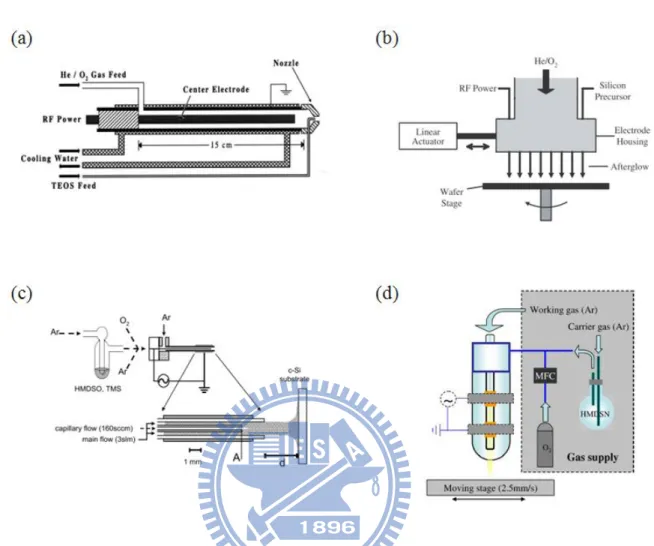
Figure 2.1 Process flow chart. ... 50
Figure 2.2 Overview of the atmospheric pressure plasma jet system. ... 51
Figure 2.3 Processing of thin film deposition. ... 52
Figure 2.4 The schematic diagram of electrode configuration. ... 52
Figure 2.5 RF power supply. ... 53
Figure 2.6 Bubbler for liquid precursor. ... 53
Figure 2.7 HMDSO monomer structure and bond strengths. ... 54
Figure 2.8 Optical emission spectroscopy. ... 54
Figure 2.9 Scanning electron microscopy. ... 55
Figure 2.10 Atomic force microscopy. ... 55
Figure 2.11 Fourier transform infrared (FTIR) spectroscopy ... 56
Figure 3.1 I-V-P curve of pure argon discharge (Ar flow rate: 5 slm). ... 57
Figure 3.2 I-V curves of Ar discharge with and without spring (Ar flow rate: 5 slm). ... 57
Figure 3.3 I-V curves of Ar, Ar+0.8%O2, and Ar+4%O2 discharge (Ar flow rate: 5 slm). . 58
Figure 3.4 Breakdown voltage of the argon plasma mixed with various oxygen concentrations (Ar flow rate: 5 slm). ... 58
Figure 3.5 The electrical characteristics curves as a function of input power for different oxygen added into argon plasma (a) P-θ; (b) P-Impedance; (c) P-Resistance; (d) P-Reactance (Ar flow rate: 5 slm). ... 59
Figure 3.6 Images for argon mixed with different concentrations of oxygen plasma and HMDSO introduced into downstream of discharge region (Ar flow rate: 5 slm; RF power: 50 W). ... 60
Figure 3.7 OES of argon mixed with different concentrations of oxygen plasma and HMDSO introduced into downstream of discharge region (Ar flow rate: 5 slm; RF power: 50 W). ... 61
Figure 3.8 OES of argon mixed with different concentrations of oxygen plasma and HMDSO introduced into downstream of discharge region at 180 to 400 nm (Ar flow rate: 5 slm; RF power: 50 W). ... 62 Figure 3.9 Species emitted of HMDSO dissociation (Ar flow rate: 5 slm; RF power: 50 W).
x
... 62 Figure 3.10 OES of argon mixed with different concentrations of oxygen plasma and
HMDSO introduced into downstream of discharge region at 400 to 700 nm (Ar flow rate: 5 slm; RF power: 50 W). ... 63 Figure 3.11 OES of argon mixed with different concentrations of oxygen plasma and
HMDSO introduced into downstream of discharge region at 700 to 900 nm (Ar flow rate: 5 slm; RF power: 50 W). ... 64
Figure 3.12 SEM images of SiOx thin film (a) cross section; (b) surface morphology on the
50 W RF power, 200 oC substrate temperature, 0 % oxygen concentration, 5 mm
treatment distance and 200 passes. ... 65
Figure 3.13 AFM of SiOx were deposited at different treatment passes (a) 4 passes; (b) 10
passes; (c) 20 passes; (d) 30 passes on the 50 W RF power, 200 oC substrate
temperature, 0.8 % oxygen concentration, and 5 mm treatment distance. ... 65
Figure 3.14 Surface and cross section SEM of SiOx showing thin films were deposited at
different treatment passes (a) 4 passes; (b) 10 passes; (c) 20 passes; (d) 30 passes on
the 50 W RF power, 200 oC substrate temperature, 0.8 % oxygen concentration, and
5 mm treatment distance. ... 66
Figure 3.15 Surface and cross section SEM of SiOx showing thin films were deposited in
different RF power (a) 35 W; (b) 40 W; (c) 50 W on 200 oC substrate temperature,
0.8 % oxygen concentration, 5 mm treatment distance and 20 passes. ... 67 Figure 3.16 Figure 3.6 Images for argon mixed with different concentrations of oxygen
plasma and HMDSO introduced into downstream of discharge region (Ar flow rate: 5 slm; RF power: 50 W)………. . 68
Figure 3.17 Surface SEM of SiOx showing thin films were deposited at different treatment
distance (a) 3 mm; (b) 5 mm; (c) 7.5 mm on 50 W RF power, 200 oC substrate
temperature, 0.8 % oxygen concentration, and 20 passes. ... 68
Figure 3.18 Surface and cross section SEM of SiOx showing thin films were deposited on
the different substrate temperatures (a) 25 oC; (b) 100 oC; (c) 200 oC (d) 300 oC on
50 W RF power, 0.8 % oxygen concentration, 5 mm treatment distance and 60 passes. ... 69
Figure 3.19 Surface and cross section SEM of SiOx showing thin films were deposited on
the different substrate temperatures (a) 25 oC; (b) 100 oC; (c) 200 oC (d) 300 oC on
50 W RF power, 4 % oxygen concentration, 5 mm treatment distance and 20 passes. ... 70 Figure 3.20 The schematic diagram of influence of substrate temperature. ... 71
Figure 3.21 Surface and cross section SEM of SiOx showing thin films were deposited
using argon plasma mixed with different oxygen concentrations (a) 0 %; (b) 0.2 %;
(c) 0.8% (d) 2 %; (e) 4 %; (f) 10 % on 50 W RF power, 300 oC substrate
xi
Figure 3.22 Deposition rate of SiOx thin films deposited on the 200 and 300 oC substrate
temperature as a function of oxygen concentration in the discharge. ... 73
Figure 3.23 IR spectra of SiOx thin films grown at substrate temperature 200 oC using
argon plasma mixed with different oxygen concentrations (a) 1400-700 cm-1; (b)
4000-2400 cm-1. ... 74
Figure 3.24 IR spectra of SiOx thin films grown at substrate temperature 300 oC using
argon plasma mixed with different oxygen concentrations (a) 1400-700 cm-1; (b)
4000-2400 cm-1. ... 75 Figure 3.25 The ratio of shoulder area to mean peak area as a function of various oxygen
concentrations mixed to argon plasma on the different substrate temperature. ... 76
Figure 3.26 Evolution of oxygen to silicon ratio and carbon concentration of SiOx thin
films deposited at substrate temperature 200 oC using argon plasma mixed with
different oxygen concentrations (passes: 20). ... 77
Figure 3.27 Evolution of oxygen to silicon ratio and carbon concentration of SiOx thin
films deposited at different substrate temperature (oxygen concentration: 4 %; passes: 20). ... 78 Figure 3.28 Image of super-hydrophobic surface. ... 79
Figure 3.29 Change in the contact angle with the surface roughness (50W, 300 oC substrate
xii
Nomenclature
P RF input power
V Measuring voltage
I Measuring current
θ Measuring phase angel between voltage and current
Z Measuring impedance
R Measuring resistance
X Measuring reactance
1
Chapter 1 Introduction
1.1 Motivation
The technology of thin film deposition has been a rapid growth into the major research
area for many years. Thin films have a number of applications in microelectronics, optics and
nanotechnology. Scratch-resistance films, e.g. SiO2, are used to protect plastic materials and
are also used as interlayers in semiconductor technology [Nowling et al., 2005]. Most of the
thin-film manufacturing processes have been fabricated by a number of methods, such as
sputtering, plasma enhanced chemical vapor deposition (PECVD) and low-pressure chemical
vapor deposition (LPCVD), among others [Plummer et al., 2000]. Among these techniques,
PECVD has demonstrated its superiority since the advantages of plasmas in materials
processing include high deposition rate and uniform glow discharge which provide the
uniform processing for a very large surface. However, the conventional PECVD process is
expensive due to the requirement of costly vacuum equipment and frequent maintenance
[Sawada et al., 1995; Pai et al., 1990].
In this study, we will focus on the development of a self-designed plasma jet system
operating at the atmospheric pressure and used for deposition technology. The coaxial APPJ is
driven by 13.56 kHz RF power in the process of depositing silicon oxide (SiOx) film on
2
as anti-scratch coating [Nowling et al., 2005], low-k dielectric layers for microelectronic
applications, as well as corrosion protective [Barchiche et al., 2009] and super-hydrophobic
coating [Yang et al., 2009; Young et al., 2008].
Most of the RF-APPJs were generated by using a mixture of helium and oxygen in SiOx
deposition, instead of the argon usually used. The major reason is that only an oxygen trace
(ca 0.01%) can easily extinguish the plasma without a proper strategy. However, a stable,
arc-free APPJ was produced with a spiral powered electrode covered by a quartz tube; this
makes the addition of oxygen (up to 10%) possible without extinguishing the discharge in our
study. In addition, argon is much cheaper than helium, and argon plasma provides better
energy transfer efficiency than helium plasma [Wang et al., 2003; Kasih et al., 2007].
Therefore, we will focus that SiOx deposition using argon mixed with oxygen RF-APPJ.
1.2 Background
1.2.1 Deposition of Silicon Oxide (SiO
x) Films and Its Applications
LPCVD (Low-Pressure Chemical Vapor Deposition), APCVD (Atmospheric-Pressure
Vapor Deposition), and PECVD (Plasma Enhanced Chemical Vapor Deposition) have been
investigated for many years for the deposition of silicon oxide (SiOx, 1<x<2) thin films
3
passivation and insulation films in semiconductor devices and electronic parts. The process of
SiOx deposition is caused by thermal decomposition of the reaction monomer (silane or TEOS)
in LPCVD and APCVD. The operating pressure of LPCVD is controlled in the range of 1 to
10 Torr and deposition temperature ranges from 400 to 800oC. The deposition temperature of
APCVD is controlled in the range of 400 to 700oC.
Plasma enhanced chemical vapor deposition (PEVD) technology, conventionally
operating at low pressure, has been investigated in the semiconductor-electronic and optical industries since the 80’s. The mechanism of thin film deposition by PECVD is shown in Figure 1.1. The gas molecules are excited, ionized, or dissociated primarily in the plasma by
electron impact. Then these excited molecules, atoms, radicals, and ions are transported and
reach the substrate by diffusion under low-pressure condition. The particles reach the
substrate surface, and further migrate and also find adsorption sites. Finally, the active
molecular react with each other, resulting in film deposition [Konuma, 2005].
The conventional PECVD, using microwave, RF, and ECR discharges to deposit SiOx
films. Various silicon-containing precursors have been oxidized, such as silane (SiH4) with
N2O, O2, or H2O. The schematic of the system configuration for an LP-PECVD reactor is
shown in Figure 1.2 [Pai et al., 1990]. Other examples of common silicon-containing
precursors used for LP-PECVD include TEOS (Si(OC3H5)4), SiCl4, SiF4 and HMDSN
4
temperature of the substrate operated in the range of 100 to 400℃. The deposition system
operated under reduced pressures, between 1.0 and 5000 mTorr [Konuma, 2005]. It is
common that inorganic precursors used deposit SiO2 film of LP-PECVD, such as silane
(SiH4). However, silane is toxic and easily ignited when exposed to air.
1.2.2 Classification of Atmospheric-Pressure Discharges
Atmospheric-pressure plasma has been shown as a great potential tool for thin film
deposition because of its low cost, low temperature and possible continuous in-line process.
Plasmas are subdivided into low temperature (LTP) and high temperature (HTP) plasmas and
a further subdivision relates to thermal (thermal equilibrium) and non-thermal plasmas (see
Table 1) [Hippler et al., 2008]. Since we are interested in applying gas discharges
(non-thermal plasma) under atmospheric-pressure condition, we further classify the
atmospheric-pressure gas discharges. The various types of atmospheric pressure plasma
[Schütze et al., 1998] include, but not limit to, transferred arc and plasma torch, corona
discharge, dielectric barrier discharge, and atmospheric-pressure plasma jet, as shown
schematically in Figure. 1.3. They are briefly introduced in the following turn.
(a) Plasma Torch
The high gas temperature (3000-20000 K) operated using plasma torch (Figure 1.3 (a)). The
5
gas molecular and usually in the thin film coating. The above are also often called thermal
plasmas and are in thermal equilibrium. However, it is not suitable for treating heat sensitive
materials because the gas temperature is too high.
(b) Corona Discharge
In the corona discharge (Figure. 1.3 (b)), plasmas are generated around the tip of a needle,
where the electric field is very large and non-uniform.
(c) Dielectric barrier discharge (DBD)
Figure 1.3 (c) which consists of two electrodes with at least one is coated with dielectrics. The
discharge is maintained through a series of microdischarges. There are two major drawbacks
for the corona discharge and the dielectric barrier discharge. One is the high breakdown
voltage (5-25 KV) and the other is the difficulty of maintaining a uniform glow like
low-pressure plasma. Since the plasmas are not uniform, it is limited for the cases where
surface need to not smooth in deposition or etching.
(d) Plasma Jet
In plasma jet (Figure. 1.3 (d)), it often consists of two coaxial electrodes through which a
mixture of gases flow. By applying 13.56 MHz RF power to the central electrode at a voltage
in the range of several hundred volts, the gas discharge can be ignited and maintained over a
fairly large range of conditions. Normally the atmospheric-pressure plasma jet is operated in the “abnormal glow” regime, in which the voltage increases with increasing current, while the
6
low-pressure plasma is often operated in the “normal glow” regime, in which the voltage
remains constant with increasing current [Schütze et al., 1998].
Schütze et al. summarized the range of breakdown voltages, plasma densities and
oxygen related species densities of different plasma sources as shown in Table 2 and Table 3.
It is clear that RF plasma jet can achieve stable discharge with much lower breakdown voltage
(50-200 V) and appreciable plasma density (1011-1012 cm-3) in the discharge region. The
densities of oxygen related species generated from plasma jet (e.g., 1016 cm-3 for both oxygen
atoms and ozone) are not the best among these plasmas, but higher density of oxygen atom
(1016cm-3) that be well suited for the PECVD of SiOx using RF-APPJ [Babayan et al., 2001].
Another important advantage of the atmospheric-pressure plasma jet is that precursors for the
thin film deposition can be introduced to the downstream of the discharge, which provides
more flexibility of controlling the processing that cannot be achieved in low-pressure plasmas.
1.3 Literature Review
1.3.1 Deposition of SiO
xFilms at Atmospheric-Pressure Condition
SiOx can be deposited using an APPJ have been considered, such as microwave
7
frequency of microwave discharge is much higher (2.54 GHz) than other discharges. There
has not been very much to use of microwave discharge for thin film deposition, because the
gas temperature is too high and it is not easy to design the equipment for thin film deposition
[Alexandrov et al., 2005]. The DBD has been widely studied for thin film deposition,
however, the substrate was usually placed on between electrodes in the deposition process. It
can be categorized into “direct AP-PECVD”, often leads to a number of complications and
problems. The substrate placed on one of the electrodes and then a mixture of reactant gases
introduced directly into the plasma region. It is easily caused complex reactions and result in
the production of many reacting species which is unpredictable. Meanwhile, the damage of
film is produced by bombardment of electrons and ions [Alexandrov et al., 2005].In contrast,
the thin film deposition using RF-APPJ has been used for “remote AP-PECVD”, the
deposition region is in the post discharge region, which can reduce the bombardment on the
films. In addition, the remote PECVD can generally allow more independent parameter
control than the direct PECVD, which may lead to better film quality. Since we are interested
in developing thin films deposited in the remote region at atmospheric-pressure, and all the
following literature surveys are restricted along this line.
The APPJ was generated by using the mixture of helium and oxygen between two
coaxial metal electrodes that were driven by 13.56 MHz RF power supply [Babayan et al.,
8
directed onto a silicon substrate kept at 115 to 350 oC. The deposition rate was discussed with
experimental parameters, such as substrate temperature, TEOS partial pressure, oxygen
concentration, and RF power. Later, five precursors were examined including HMDSN,
HMDSO, TMDSO, TMCTS and TEOS by using helium mixed with 2% oxygen plasma and
the APPJ was driven by RF 27.12 MHz, as shown in Figure 1.4 (b). The results reported that
high quality films without visible defects, such as cracking or chalkiness, could be obtained
with precursors at specific deposition rats. However, the material exhibits poor abrasion
resistance using TMDSO. They also found that coating, close to silicon dioxide (SiO2)
structure, with minimal OH and CHx impurities; provide superior hardness and abrasion
resistance [Nowling et al., 2005].
As mentioned earlier, most of the RF-APPJs were generated by using the mixture of
helium and oxygen. Helum and argon are used as the discharge gas in the RF-APPJ system.
The other interesting thing is that, as oxygen is directly added into plasma, only helium is
used, except the work done by [Ha et al., 1995]. The major reason is that only trace of oxygen
(ca 0.01 %) can easily extinguish the plasma with proper strategy. In addition, argon is much
cheaper than helium, and argon plasma provides better energy transfer efficiency that helium
plasma under the same working condition [Wang et al., 2003; Kasih et al., 2007]. Argon
RF-APPJ system has been recently applied to deposit the SiOx film without oxygen contained
9
2009]. Rather, the oxygen is mixed with the precursor at the downstream of the APPJ. The
thin film deposition rate increases significantly with oxygen flow rate; however, too much
oxygen caused deposition rate decrease slightly since oxygen is an electronegative gas which
could cause electron energy loss [Park et al., 2001]. Finally, Table 4 is shown as summary of
important features for the SiOx film deposited using APPJ at remote region. It is interesting
and important to understand the influence of the oxygen addition on the SiOx film deposition.
1.4 Specific Objectives and Organization of the Thesis
For this study, the fundamental characteristic of APPJ discharge and its application in the
SiOx deposited were investigated. The specific objectives of the present thesis can be
summarized as followed:
1. To diagnose the discharge characteristics of argon and argon mixed with oxygen (up
to 10 %), including electrical and optical properties.
2. To deposit SiOx films on the substrate using RF-APPJ in a stable, arc-free discharge.
3. To compare distinct operational factors to discuss the properties of thin film,
including treatment passes, RF input powers, distances, substrate temperatures, and
oxygen concentrations.
4. To measure SiOx films properties using a Fourier transform infrared spectrometer
10
the drop shape method for contact angle measurement instruments, and an X-ray
11
Chapter 2 Experimental Methods
In this study, we have designed and constructed the system for SiOx film deposition using
RF-APPJ. Plasma diagnostic measured, including electrically (IV characteristics, impedance
analysis), optically (OES) and plasma temperature. For thin film deposition, the SiOx films
were deposited on P-type silicon substrates which were cleaned first. With distinct
experimental factors, the properties of SiOx films were analyzed by Fourier-transform infrared
spectrometer (FTIR), atomic force microscope (AFM), scanning electron microscope (SEM),
and X-ray photoelectron spectroscopy (XPS). The process flow chart of RF-APPJ system
used for thin film deposition as shown in Figure 2.1.
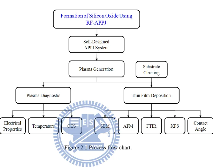
2.1 Experimental Facility
A schematic of the experimental setup of the proposed APPJ system driven by a 13.56
MHz RF power supply is shown in Figure 2.2. The experimental facility included 4 parts, RF
power supply, matching and lines, gas feeding system, and electrode assembly. And the
12
2.1.1 APPJ System
A steel spring with a diameter of 4 mm was inserted between the stainless steel tube
(outer diameter 3.2 mm) and a quartz tube (inner diameter 4 mm). Note the spring was in
direct contact with the stainless steel tube, which both together was used as the power
electrode. An aluminum tube with an inner diameter of 6 mm and 20 mm in length was placed
outside the quartz tube and used as the ground electrode.
The discharge gas (argon or
argon mixed with oxygen) was passed through the space between the inner and
outer electrodes following the spiral spring. The quartz tube extruding 5 mm from
the end of electrodes was 1 mm in thickness and was used as the dielectrics to
prevent the arc formation. The schematic diagram is shown in
Figure 2.4.2.1.2 RF Power Supply
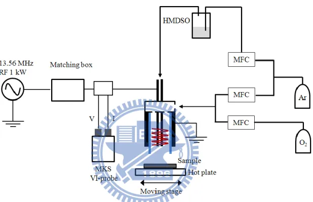
The RF power was provided by a Dressler (model CESAR 1310) is shown in Figure 2.5.
The frequency is 13.56 MHz, max output power is 1000 W into a 50 Ω load; it is connected to
the APPJ through a matching box. Basic discharge parameters, such as the input RF power,
RF voltage, RF current and phase angle, are measured by an RF impedance analyzer (MKS
13
2.1.3 Matching Box
Matching Box used L-network the match way (RG-213/U) to make the connection after
50 coaxial cable line effectively transmits the RF Power Generator electromagnetic wave
to the APPJ chamber.
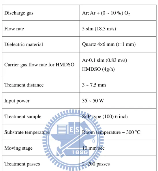
2.1.4 Gas Feeding System
The argon and oxygen gas (1/4 in the Teflon tube) connected the flow meters from the
high-purity high-pressured steel cylinder. The flow rates of different gases were controlled by
manually adjustable flow meter. The discharge gases, argon mixing with oxygen were fed into
the gap between two electrodes to generate plasma. In this study, the flow rate of argon kept at
5 slm and mixed with various oxygen flow rates in the range of 0 to 0.5 slm (0 to 10 vol. %).
The organic silicon-containing precursor, HMDSO (Hexamethyldisiloxane, purchased
from ACROS Organics, Germany, at 98% purity), is liquid phase and high vapor pressure at
the room temperature. The properties of HMDSO are shown in the Table 5. The carrier gas,
argon, flow rate was kept at 0.1 slm and fed into the bubbler which contain HMDSO liquid
(Figure 2.6), and carrier gas and reactant vapor of monomer were delivered into
post-discharge region. The monomer gas flow rate was kept at 4 g/h. The monomer
14
2.2 Experimental Instrumentation
The plasma generated using RF 13.56 power supply at atmospheric pressure, and the
experimental instrumentation used to measure the properties of plasma such as V-I probe and
oscilloscope for observation the plasma electrical. The species formations of plasma were
detected by optical emission spectroscopy in the range of 180 to 900 nm. In the other hand,
the film’s thickness was measured by scanning electron microscope. The understanding of
functional groups of SiOx films were analyzed by Fourier transform infrared spectroscope.
Atomic force microscope used for measuring the surface roughness and observing the film’s
morphology. The surface chemical compositions were analyzed using X-ray photoelectron
spectroscopy. The hydrophobic property of the SiOx film’s surface were measured using a
contact angle machine, and the hardness was determined using the pencil test. Table 6
summarizes various instruments which were used for the measurements.
2.2.1 V-I Probe for Electrical Property Measurements
The V-I probe was provided by a MKS (model V-I probe 4100). V-I probe was one kind
of RF Impedance Analyzers. The basic discharge parameters, such as RF voltage, RF current
and phase angle were measured, and then by the computer, pushing back the impedance,
15
provided a best of a very useful tool, can also avoid some unnecessary depletion of power.
2.2.2 OES (Optical Emission Spectroscopy) for Species Identification
Measurements
The spectral optical emission intensities of RF-APPJ were measured using a
monochromator (PI Acton SP 2500) with a photomultiplier tube (Hamamatsu R928) which
was mounted on a mobile 3-D table (see Figure 2.8). The spectral range was 180-900 nm with
120 g/mm grating (Hologrphic, 300 nm Blaze and 500 nm Blaze). OES measuring is
identifying which particles species emits radiation. In addition, a spectroscopy software
package, named Plasus SpecLin, was used to finding specific lines in the spectra and excited
species level change.
2.2.3 Scanning Electron Microscope (SEM) for Cross-section Morphology
Observation of Thin Film
The surface and cross-section morphology observed using scanning electron microscope
(Hitachi S-4700I) is shown in Figure 2.9. SiOx images by scanning it with a high-energy beam
of electrons and producing signal of secondary electron that contains information about the
16
2.2.4 Atomic Force Microscope (AFM) for Surface Topology Observation
The AFM images were obtained in Veeco Dimension 5000 Scanning Probe Microscope
(Figure 2.10), which consisted of a micro-scale cantilever with a sharp tip (probe) at its end
that is used to scan the SiOx film’s surface. The cantilever was typically silicon or silicon
nitride with a tip, and the tapping mode was used. The tip is not in contact directly with the
surface and tip oscillated frequently when moved toward the surface until it begins to lightly
touch. The tapping mode provides the resolution of 1 to 5 nm, it is lower than contact mode
but the surface does not damaged easily. The image we obtained could 2D, 3D, and also the
roughness data can be measured.
2.2.5 Fourier Transform Infrared Spectroscope (FTIR) for Surface Bonding
Identification
Fourier transform infrared (FTIR) spectroscopy is a measurement technique for
collecting infrared spectra when vibration and rotating of molecule absorbed or transmitted
infrared radiation. In this study, we analyzed the chemical structure and composition of SiOx
film with Perkin Elmer RX1 (Figure 2.11), scan range is from 4000 to 400 cm-1 with
resolution of 4 cm-1 and each spectrum was obtained from an average of 32 scans.
17
and Bonding Identification
X-ray Photoelectron spectroscope (XPS) is a surface characterization spectroscopy. It is
a spectroscopic technique to identify the elemental composition, and also measures empirical
formula, chemical state and electronic state of the film’s surface. We analyzed the surface
element and compound with Ulvac-PHI 1600 (Mg anode at 250W and 15KV, 1253.6 eV, the
electron talke-off angle respect to the SiOx film surface was 45o, chamber pressure below 2×
10-8 Torr).
2.2.7 Contact Angle Measurement Device
The surface of thin film was measured by contact angle measuring device using
commercial KRUSS Easy Drop optical system (KRUSS GmbH-Germany). Distilled water
drops of 10 μl were used as test liquid in our study. The values of the static contact angle
obtained from Laplace-Young curve fitting based on the imaged sessile water drop profile.
2.2.8 Pencil Hardness Test
The hardness of SiOx was determined using the pencil test (B-3084T). It have consists of
14 pencils, ranging in hardness from 6H to 6B. The hardest is a 6H, followed by 5H, 4H, 3H,
18
over the deposited specimen. The one grade pencil be selected to start with scratching the
surface, then test down the pencil grades until the first pencil that does not scratch the coating.
2.3 Experimental Procedures and Test Conditions
The self-designed APPJ system is shown in Figure 2.2. The plasma was generated
between the electrodes using an RF 13.56 (MHz) power supply.The plasma diagnostics used
included electrical (IV characteristics, impedance analysis), optical (OES) and gas
temperatures. Testing conditions for the former confirmed the stability of plasma.
In this study, we used a P-type silicon wafer for use in the substrate for depositing SiOx
films. The procedures for sample preparation are shown as follows:
(a) Cut wafer to 10 × 20 mm2 and place in ultrasonic cleaner in acetone for 10 min.
(b) Wash the sample with de-ionized water
(c) Ultrasonic clean in ethyl alcohol for 10 min
(d) Wash the sample with de-ionized water
(e) Dry the sample with nitrogen gas
The precursor was fed into the downstream post-discharge, and reacted with plasma. Then,
the silicon substrates were placed on the heating plate which moved back and forth by a
moving stage, passed through the plasma jet and thin films deposited on the substrates. With
19
The flow rate of the discharge gas was kept at 5 slm (18.3 m/s) for all conditions and the
flow rate of carrier gas for HMDSO was kept at 0.1 slm (0.8 m/s). SiOx films were deposited
at various testing conditions, including treatment passes, RF input powers (35-50 W),
distances (3-7.5 mm), substrate temperatures (room temperature - 300oC), and oxygen
concentrations (0-10 %). All of the samples deposited on the moving stage were fixed at 10
mm/s. Argon mixed with various oxygen concentrations (0 to 10%). The testing condition of
RF-APPJ for SiOx deposition has been summarized in Table 7.
20
Chapter 3 Results and Discussion
3.1 Electrical Characterization of the APPJ System
An APPJ, using RF power, has been developed to produce a homogeneous glow, and
discharge parameters have been discussed [Li et al., 2006].
The impedance:
I V
Z (3-1)
The resistance: cos
I V R (3-2)
The reactance: sin
I V X (3-3)
The phase angle:
R X
(3-4)
The discharge characteristics of APPJ can be discussed by relationships among Irms, Vrms,
power, impedance, and phase angle. A typical I-V discharge characteristic of pure argon at a 5
slm flow rate is shown in Figure 3.1. Input power was controlled in the range of 0 to 60W, and
dark discharge occurred before the voltage breakdown of 580 V. After voltage breakdown, the
current and voltage increased linearly (abnormal discharge) and plasma was generated. In
addition, Figure 3.2 illustrates voltage and input power for pure argon plasma, with and
without spring as a function of current, respectively. Without the use of a spiral electrode, the
breakdown voltage was as high as 718 V. After the breakdown process, the voltage drop to
433 V and then increased with the rising current. A stable discharge was observed as
21
electrical field occurred at the smaller electrode gap when using a spiral electrode, results
showed a decrease in breakdown voltage. Figure 3.3 illustrates voltage for argon mixed with
various oxygen concentrations in plasma as a function of current. The electrical properties of
argon mixed with oxygen, discharged with the use of a spiral electrode, were similar to pure
argon discharge. Only the breakdown voltage increased because an electronegative gas, such
as oxygen, was added to the plasma [Park et al., 2001]. The measured minimum voltage
required to sustain the argon mixed with oxygen plasma, which would be increased by
increasing the oxygen concentration, are shown in Figure 3.4. The relationship between input
power and the other electrical properties, such as phase angle, impedance, resistance, and
reactance, are shown in Figure 3.5. Before plasma is generated, the coaxial electrode is like a
pure capacitive and the current leaded the voltage nearly 90o in phase. When input power was
increased continuously, the phase angle decreased slightly in the range of 1o (Figure 3.5 (a)).
It is different than the greater phase shift of a current leading the voltage of pure argon or that
mixed with oxygen plasma using RF-APPJ because of the inner quartz tube between the
power and grounded electrode [Wang et al., 2003]. The impedance decreased with input
power and increased with oxygen added (Figure 3.5 (b)). The impedance is combined with
resistance and reactance terms [Zhu et al., 2005], resistance increased in the range of 2 to 3 Ω but the decrease in reactance was in the range of 3 to 8 Ω with input power (Figure 5 (c) and (d)). Therefore, the impedance trend was to decrease with the decrease in reactance.
22
3.2 Visual Observation and Optical Emission Spectral Analysis of APPJ
Typical images for argon mixed with plasma of different oxygen concentrations and
HMDSO was fed into the downstream of the discharge are shown in Figure 3.6. For pure
argon discharge, the plasma plume gave an emission of violet light. When HMDSO was fed
into the downstream of the discharge region, the color of the plasma plume changed to blue.
The color of the plasma plume appears to darken slowly when oxygen was fed into the plasma.
The changes in the color of the plasma can be explained clearly by OES measurement and
relative optical emission shown in the range of 180 to 900 nm in Figure 3.7. Then the OES
was analyzed by dividing it into three spectral ranges, 180 to 400 nm, 400 to 700 nm, and 700
to 900 nm to compare pure argon, argon mixed with oxygen, and HMDSO that was
introduced downstream of the discharge. The OES reveals the presence of excited fragments
of the monomer structure ((CH3)3-Si-O-Si-(CH3)3), such as Si, Si-O, CH, and C2 [Granier et
al., 2002; Wang et al., 2005; Chen et al., 2006]. The Si-C and C-H in the monomer are easily
broken by an electron or a high energy metastable radical, since the bond energy of Si-C (4.6
eV) and C-H (3.5 eV) is lower than Si-O (8.3 eV). Excited Si atom emission was evident from
the argon plasma and HMDSO introduced downstream of the discharge, and there was a
relative line decay when oxygen was fed into the plasma, as shown in Figure 3.8. The excited
23
argon easily generates more electrons of higher energy radicals than oxygen added into
plasma. Due to the fact that oxygen is characteristic of an electronegative, electrons generated
from plasma easily decrease. This phenomenon is likely to decrease the ability of a monomer
to be polymerized. Similarly, the detected line of Si-O fragments at 216 to 290 nm is shown in
Figure 3.9. The spectral, ranging from 400 to 700 nm, presents carbon-containing species (CH,
C2) detected from argon plasma and HMDSO introduced downstream of the discharge, and
the relative emission appeared in the emission of a blue light region of 400 to 500 nm (Figure
3.10). In addition, the region of 700 to 800 nm was detected from excited Ar atom emission
(Figure 3.11). Pure argon discharge exhibited the highest intensity of the other test cases.
When oxygen was fed into plasma or HMDSO was introduced downstream of the discharge,
the emission intensity of the argon region decreased, partially due to the energy needed to
dissociate or ionize the oxygen and HMDSO molecules.
3.3 Surface Morphology and Deposition Rate of Thin Film
The surface morphology of SiOx films was observed using SEM, and the thickness of the
films was measured from the SEM cross section images. Thin films were deposited on the
substrate using a moving stage controlled at 10 mm/s per pass and an inner diameter tube of 4
mm. The residence time of one pass is 0.4 s. Figures 3.12 (a) and (b) show SEM cross section
24
time was 80 s for 200 passes and the thickness of the thin film was 120 nm. Thus, the
deposition rate was 90 nm/min. The roughness of the thin films measured by AFM and the
scan size of the samples was 2x2 μm. In addition, the plasma temperature of 100oC was
measured at 5 mm from the exit of the quartz tube using a K type thermocouple.
3.3.1 Effect of Number of Treatment Passes
The surface morphology of SiOx thin films observed under various treatment passes are
shown in Figure 3.13. The morphology of the surface structure changed from 4 passes to 30
passes. The beginning of thin film grown on the surface can be found via 4 passes and the
surface roughness was 2.2 nm (Figure 3.13 (a)). The thickness of the thin films measured
about 100, 200, and 350 nm via 10, 20, and 30 treatment passes, respectively. SEM surface
images are shown in Figure 3.14. The particle size and roughness of the thin films also
increased with the increasing number of treatment passes.
3.3.2 Effect of Input Power
Figure 3.15 shows the effect of the RF power on the thickness of thin films from 35 W to
50 W. If the RF power was less than 35 W, the deposition rate of the thin film was too slow to
25
corresponds to the increase in the concentration of active species such as excited argon atoms
or excited molecules of oxygen in the plasma stream from the discharge region [Alexandrov
et al, 2005]. The concentration of argon metastable excited atoms increased with the increase
of RF power and caused partial dissociation and formation of silicon-containing active species
which further enhanced the deposition rate of thin films.
3.3.3 Effect of Treatment Distance
Figure 3.16 shows the effect of the thickness of thin films on various treatment distances
ranging from 3 mm to 7.5mm (from the end of the quartz tube). The thickness of the thin
films deposited exhibits a strong dependence on treatment distance. HMDSO monomer
dissociated via plasma formed the silicon-containing active species and further polymerized
on the surface. If the substrate was close to the exit of the monomer, the active species
increased and the deposition rate was enhanced. Contrarily, the active species were easily
quenched in the ambient via far distance treatment. However, the 3 mm treatment distance
was not better for higher deposition rate where the thin film exhibited rough surfaces and
loose structure of big particles, as shown in Figure 3.16 (a) and Figure 3.17 (a).
26
3.3.4 Effect of Substrate Temperature
The effect of various substrate temperatures heated in the range from room temperature
to 300oC, and thin films deposited when 0.8% oxygen was added to the discharge are shown
in Figure 3.18. Not thin film formation, but polymerization of the HMDSO at low substrate
temperatures was found, as shown in Figures 3.18 (a) and (b). There was no solid-state
structure of thin film formation and a grease surface presented on the substrate. Figure 3.19 (a)
shows the same situation when argon is mixed with 4% oxygen and added into the discharge.
In addition, it is interesting to compare the thickness of thin films at the various substrate
temperatures.
The thickness of thin films deposited in the same treatment passes showed a strong
negative dependence on the substrate temperature and many authors have discussed this
situation using atmospheric pressure plasma [Babayan et al., 2001; Huang et al., 2009]. The
sticking coefficient of the active molecule species formed from the plasma region decreased
as substrate temperature increased. The ability of molecules to absorb the substrate reduced,
but thermal diffusion of the molecules was enhanced at high substrate temperatures to diffuse
into the suited sites of the thin film and caused dense film formation, the schematic diagram
27
3.3.5 Effect of Oxygen Concentration in the Discharge
The effect of film characteristics on deposition, using argon plasma mixed with
various oxygen concentrations, is shown in Figure 3.21. The thickness and surface
morphology of thin films deposited in the same treatment passes showed a strong positive
dependence on oxygen concentration. The thickness of film deposited using pure argon
plasma was hard to measure accurately. Thus the deposition rate was calculated to be 37.5
nm/min via increasing passes to 200. When oxygen added into argon plasma increased to 0.2
and 0.8%, the deposition rate was 200 and 275 nm/min, respectively. Surface roughness of
deposited pure argon plasma was 1.38 nm. When oxygen introduced into argon plasma
increased to 0.2 and 0.8%, the roughness was 5.26 and 29.8 nm, respectively. High
mechanical strength with a smooth and transparent surface of SiOx thin film can be formed
using argon plasma mixed with oxygen below 0.8% at 300oC substrate temperature. However,
oxygen addition was more than 2 %, particles of a hundred nanometer scale were observed
and films lost their transparency, powdery structure formed (see Figure 3.21 (d) to (f)). The
possible results of reaction between the silicon-containing species and oxygen, and further
cause nucleation in gas phase [Kasih et al., 2007].
Figure 3.22 shows the relationship between the deposition rate and oxygen concentration
in the discharge at various substrate temperatures. Oxygen plays an important role in the
28
et al., 1995; Zhu et al., 2005] to SiOx films. The oxygen radicals generated from argon mixed
with oxygen at discharge, and excited oxygen promote decomposition of monomer molecules.
Therefore, the deposition rate increases by adding oxygen.
Further hardness testing briefly is presented in Table 8 under variation conditions. For
the 200 oC substrate temperature, the lowest deposition rate (90 nm/min) of pure argon plasma
has a rating of 5H in thickness of 100 and 300 nm. However, the film exhibited a lower pencil
hardness of HB if oxygen added to 0.8%. For the 300 oC substrate temperature, the deposition
rate was decreased from 1200 nm/min to 275 nm/min and the hardness evidently raised to 4H.
3.4 Bond Structure Analysis by FTIR
The bond structure of SiOx film was analyzed by Fourier Transform Infrared (FTIR)
Spectroscopy. The resolution of 4 cm-1 for all spectra and each spectrum was obtained from an
average of 32 scans. SiOx exhibits three characteristic absorption peaks at rocking (450 cm-1),
bending (800 cm-1), and asymmetric stretching (1075 and 1150 cm-1). An organic component
of the absorption peak exhibits at 840 cm-1 (Si-CH3 stretching in the Si-(CH3)3 group) and 800
cm-1 (Si-CH3 stretching in the Si-(CH3)2 or the Si-(CH3) group). The Si-CH3 bending mode at
1273 cm-1 and the CH3 stretching mode at around 2960 cm-1 can be observed. The broad
absorption bands at around 3400 cm-1 are attributed to OH bending and absorption at 940 cm-1
29
the deposition films formed by adding various oxygen concentrations was analyzed by FTIR
at 200 and 300oC as shown in Figure 3.23 and Figure 3.24, respectively. It can be seen that
organic components (CH3 or Si-CH3 groups) changed with the addition of oxygen and are
show in Figure 3.23 (a) and Figure 3.24 (a). When oxygen gas is added into the plasma region,
and atom oxygen radicals and excited oxygen molecules are generated, it can partially
decompose the carbon-containing groups of HMDSO monomer in the gas-phase or substrate
surface [Sawada et al., 1995; Wavhal et al., 2006]. Therefore, the absorption peaks related to
thin film carbon were decreased by adding oxygen into the plasma.
Many authors who have discussed the degree of SiOx thin film porosity use the ratio of
shoulder area at 1150±10 cm-1 to mean peak area at 1075±5 cm-1 [Nowling et al., 2005]. The
relationship between degree of porosity and addition of oxygen is shown in Figure 3.25, and
the trend is shown that the more oxygen that is added to the plasma, the higher the degree of
porosity of film obtained. Meanwhile, higher substrate temperatures evidently decrease the
porosity of the film. It can be interpreted as a higher deposition rate easily causes a higher
degree of porosity. In addition, the OH group of films was measured at around 3400 cm-1, as
shown in Figure 3.23 (b) and Figure 3.24 (b), which attributed to OH bending during and after
deposition, and following exposure to atmospheric vapor [Raballand et al., 2009]. The peak,
at 3400 cm-1, increased absorption with the addition of oxygen at 200oC substrate temperature.
30
on the substrate at a temperature of 300oC clearly disappeared.
3.5 Surface Composition Analysis by XPS
Surface composition was analyzed by x-ray photoelectron spectroscopy and the surface
of each sample was cleaned by ion gun spattering for 30 s. We compared the various oxygen
concentrations added to the plasma to the effects of the oxygen-to-silicon ratio (O/Si) and
carbon-to-oxygen ratio (C/O), as shown in Figure 3.26. It can be seen that the O/Si ratio
increased with the increase of oxygen concentration. The O/Si ratio of the film deposited
using pure argon plasma was low, 1.31. This may have been caused by a fraction of the
monomer being formed from post discharge of pure argon plasma, and a decrease in
polymerization reaction ability. C/O ratio groups do not reduce efficiently (18.3%) because
there is not enough excited oxygen to promote decomposition of the monomer. Adding
oxygen concentration increased O/Si ratio to 1.56 at 4% oxygen concentration but lowered
slightly to 1.51 at 10% oxygen concentration. C/O ratio decreased with the increase of oxygen
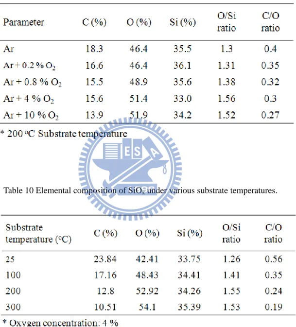
concentration. The element composition of thin films under various oxygen concentrations is
shown in Table 9. In addition, the relationship between films deposited at various substrate
temperatures, and O/Si ratio and C/O were also analyzed using 4% oxygen concentration
added to plasma, as shown in Figure 3.27. At a lower substrate temperature, 25oC, thin film
31
concentration evidently decreased from 23.8% to 10.5% when the substrate temperature
increased from 25oC to 300oC. The element composition of thin films under various substrate
temperatures is shown in Table 10. It could be because the thermal decomposition of the
carbon-containing group at higher substrate temperatures [Huang et al., 2009].
3.6 Contact Angle Measurements
SiOx thin film is one material available for producing a hydrophobic and
super-hydrophobic coating [Yang et al., 2009; Ji et al., 2009]. Its application includes
self-cleaning and reduced contamination. A rough surface and low surface energy are
important to enhance hydrophobicity of the surface. In our study, surface roughness changes
can be accomplished by controlled distinct experimental parameters, including oxygen
concentrations, substrate temperatures, and treatment passes. The SiOx film with a low surface
energy functional group (-CH3), was measured by an FTIR instrument as shown in Figure
3.24 (a). The image of silicon substrate was treated and untreated as shown in Figure 3.28, the
SiOx with super-hydrophobic surface of right side. Figure 3.29 shows that the effect of the
water contact angle of deposited films depends on controlling various oxygen concentrations
being added into the discharge. When oxygen was added to 0.2%, the surface roughness of the
film was 5.3 nm and the measurement of contact angle was 81.4o. A super-hydrophobic
32
150o, and the surface roughness was 29.7 nm. As the oxygen added to 2% (or more), although
the measurement of contact angle was higher than 150o, the powdery structure was formed
33
Chapter 4 Concluding Remarks
4.1 Summary
The deposition of SiOx films, from pure HMDSO, by means of argon mixed with oxygen
atmospheric-pressure plasma jet was studied. SiOx deposited under various test conditions,
and properties of thin film have been discussed. Results show that various oxygen
concentrations added into argon plasma and substrate temperature greatly affected the
properties of SiOx film. A higher deposition rate was obtained at higher oxygen concentrations,
but more oxygen addition (2-10%) caused the highly porous structure formation, the particles
of a hundred nanometer scale were observed. Meanwhile, the O/Si ratio increased with
oxygen addition.
It was found that the various substrate temperatures controlled in the deposition process
evidently affected the deposition rate, degree of porosity, and chemical composition of the
SiOx. Deposition rate decreased with increasing substrate temperature. Lower degree of
porosity and less OH in the film was obtained under the higher substrate temperatures, and
SiOx provided the excellent hardness surface. Carbon atoms in the film decreased, it could be
because the thermal decomposition of the carbon-containing group at higher substrate
temperatures.
34
films with the function group, -CH3, which may enhance the hydrophobicity of the surface. A
super-hydrophobic surface, water contact angle greater than 150o, formed when oxygen was
added to 0.8% (or more).
4.2 Recommendations of Future Work
According to this study, the future work is suggested as following,
1. We expect to find the suited condition to deposit the super-hydrophobic surface of SiOx
films on the glass as well as high UV-VIS transmission;
2. To compare the silicon oxide using various precursors, such as HMDSN, TEOS;
3. To compare the characteristic of SiOx films when oxygen be added in the post-discharge
region with the carrier gas for precursor;
4. The refractive index and dielectric constant of SiOx film shall be measured. And further,
SiOx films can be employed for a lot of applications in different fields such as corrosion
protective coating;
5. We shall develop the planar RF-APPJ system for continuous in-line processing of large
35
References
[1] Alexandrov S.E., McSporran N., and Hitchman M.L.,” Remote AP-PECVD of silicon dioxide films from hexamethyldisiloxane (HMDSO)”, Chemical Vapor Deposition, Vol. 11, Issue 11-12, pp. 481-490, 2005.
[2] Babayan S.E., Jeong J.Y., Tu V.J., Park J., Selwyn G.S., and Hicks R.F., “Deposition of
silicon dioxide films with an atmospheric-pressure plasma jet”, Plasma Sources Science
and Technology, Vol. 7, Issue 3, pp. 286-288, 1998.
[3] Babayan S.E., Jeong J.Y, Schütze A., Tu V.J., Moravej M., Selwyn G.S., and Hicks R.F., “Deposition of silicon dioxide films with a non-equilibrium atmospheric-pressure plasma jet”, Plasma Sources and Science Technology, Vol. 10, Issue 4, pp. 573-578, 2001.
[4] Barchiche C.E., Rocca E. and Hazan J., “Corrosion behaviour of Sn-containing oxide
layer on AZ91D alloy formed by plasma electrolytic oxidation”, Surface and Coatings
Technology, Vol. 2, Issue 17, pp. 4145-4152, 2009.
[5] Benedikt J., Raballand V., Yanguas-Gil A., Focke K., and von Keudell A., “Thin film deposition by means of atmospheric pressure microplasma jet”, Plasma Physics and Controlled Fusion, Vol. 49, Issue 12B, pp. B419-B427, 2007.
[6] Bour J., Bardon J., Aubriet H., Frari D.D., Verheyde B., Dams R., Vangeneugden D.,
36
atmospheric pressure for corrosion protection”, Plasma Processes and Polymers, Vol. 5,
Issue 8, pp. 788-796, 2008.
[7] Dowling D.P., Ramamoorthy A., Rahman M., Mooney D.A., and MacElroy J.M.D., “Influence of atmospheric plasma and gas composition on the properties of deposited siloxane coating”, Plasma Processes and Polymers, Vol. 6, pp. S483-S489, 2009. [8] Fujino K., Nishimoto Y., Tokumasu N., and Maeda K., “Silicon dioxide deposition by
atmospheric pressure and low-temperature CVD using TEOS and ozone”, Solid-State
Science and Technology, Vol. 137, Issue 9, pp. 2883-2887, 1990.
[9] Granier A., Vervloet M., Aumaille K., and Vallee C, “Optical emission spectra of TEOS and HMDSO derived plasmas used for thin film deposition”, Plasma Sources Science and Technology, Vol. 12, Issue 1, pp. 89-96, 2003.
[10] Ha H.K., Inomata K., and Koinuma H., “Plasma chemical vapor Deposition of SiO2 on
air-exposed surfaces by cold plasma torch”, Journal of the Electrochemical Society, Vol.
142, Issue 8, pp. 2726-2730, 1995.
[11] Hippler R., Kersten H., Schmidt M., and Schoenbach K.H., Low Temperature
Plasmas-Fundamentals, Technologies and Techniques, Vol. 2, 2nd, Wiley-VCH, 2008.
[12] Huang C., Liu C.H., Su C.H., Hsu W.T., and Wu S.Y., “Investigation of
atmospheric-pressure plasma deposited SiOx films on polymeric substrates”, Thin Solid
37
[13] Huang C., Liu C.H., Wu S.Y., “Surface characterization of the SiOx films prepared by a
remote atmospheric pressure plasma jet”, Surface and Interface Analysis, Vol. 41, Issue 1,
pp. 44-48, 2009.
[14] Ji Y.Y., Kim S.S., Kwon O.P., and Lee S.H., “Easy fabrication of large-size
superhydrophobic surfaces by atmospheric pressure plasma polymerization with
non-polar aromatic hydrocarbon in an in-line process”, Applied Surface Science, Vol.
255, Issue 8, pp. 4575-4578, 2009.
[15] Kasih T.P., Kuroda S.I., and Kubota H., “A nonequilibrium, atmospheric-pressure argon
plasma torch for deposition of thin silicon dioxide films”, Chemical Vapor Deposition,
Vol. 13, Issue 4, pp. 169-175, 2007.
[16] Konuma M., Film Deposition by Plasma Techniques, Springer-Verlag, Heidelberg, 1992
[17] Li S.Z., Lim J.P., Kang J.G., and Uhm H.S., “Comparison of atmospheric-pressure
helium and argon plasmas generated by capacitively coupled radio-frequency discharge”,
Physics of Plasma, Vol. 13, Issue 9, 2006.
[18] Matsuura M., Hayashide Y., Kotani H., and Abe H., “Film characteristics of APCVD
oxide using organic silicon and ozone”, Japanese Journal of Applied Physics Part 1, Vol.
30, Issue 7, pp. 1530-1538, 1991.
[19] Morent R., Geyter N.D., Jacobs T., Vlierberghe S.V., and Dubruel P., “Plamsa-polymerization of HMDSO using an atmospheric pressure dielectric barrier
![Figure 1.1 Schematic representation of the PECVD reaction process [Konuma, 2005].](https://thumb-ap.123doks.com/thumbv2/9libinfo/8252245.171743/61.892.196.776.526.993/figure-schematic-representation-pecvd-reaction-process-konuma.webp)