Physical Characterization and Electrical Properties
of Sol-Gel-Derived Zirconia Films
Hsin-Chiang You,a Fu-Hsiang Ko,b,
*
,zand Tan-Fu Leia a
Institute of Electronics Engineering, National Chiao Tung University, Taiwan b
Institute of Nanotechnology, National Chiao Tung University, Taiwan
We have developed a simple method for the preparation of ZrO2 ultrathin films; it involves a sequence of ZrCl4 precursor preparation in an ice bath, sol-gel spin-coating processing, baking, and annealing. The film thickness was controllable and tunable by altering the ZrCl4/hexanol ratio. High-resolution transmission electron microscopy共TEM兲 and thermal desorption spectrometry indicated that the fabricated ultrathin film was thermally stable at annealing temperatures as high as 900°C. Diffraction patterns of TEM indicated that the films obtained at various annealing temperatures were amorphous. Electron spectroscopy for chemical analysis 共ESCA兲 demonstrated an increase in the intensity of the signal for the Zr–O bonds upon increasing the annealing temperature, whereas those for the signals of carbon and chlorine decreased. The ESCA and TEM analyses also suggested that the thickness of the silicon dioxide film increased upon increasing the annealing temperature. The electrical properties, such as the breakdown field共12.5 MV/cm兲 and the gate current density 共⬍10−7A/cm2兲, of the sol-gel-derived ZrO
2ultrathin films obtained after annealing at 900°C suggested that they were good electrical insulators. These ZrO2thin films are expected to behave as capacitors and as coatings for insulating films.
© 2006 The Electrochemical Society. 关DOI: 10.1149/1.2186182兴 All rights reserved.
Manuscript submitted June 14, 2005; revised manuscript received January 26, 2006. Available electronically April 11, 2006.
Silicon technology has formed the basis of microelectronics and electronics systems for more than 30 years. In terms of productivity, the density of devices on a silicon chip has followed Moore’s law, doubling about every two or three years since about 1980. Many researchers are interested in scaling down electronics devices so that they may perform at higher speeds and be prepared at lower costs. Conventional SiO2gate dielectrics are reaching their physical thick-ness limit共1.5 nm兲; they cannot be used as complementary meta-loxide semiconductor devices because of the high direct-tunneling current and poor reliability. For further scaling of devices, it has been proposed that SiO2be replaced by high-k dielectric constant materials, such as ZrO2, HfO2, Ta2O5, Al2O3, TiO2, and silicates 共ZrSixOy and HfSixOy兲.1-8. In fact, dielectric films having higher
permittivity allow the use of thicker films of equivalent electrical thickness as silicon dioxide; this situation reduces the leakage cur-rent and improve the reliability of the dielectric films.
The most important properties of high-k dielectric materials that are necessary to maintain continuous increases in device perfor-mance and density are their low leakage current, low equivalent oxide thickness共EOT兲, high breakdown strength, high thermal sta-bility, and gate electrode compatibility. The EOT, teq, of an alterna-tive high-k dielectric can be obtained from the simple equation
teq=共Kox/Khigh-k兲thigh-k
where Kox and Khigh-k are the dielectric constants of silicon oxide and the high-k dielectric, respectively, and thigh-k is the physical thickness of the high-k material. Future downscaling will require high-k materials in which EOT values are reduced to nearly 0.7 nm.9 We must bear in mind that many of the characteristics of these
high-k dielectrics—such as their breahigh-kdown mechanism and hysteresis
phenomena—are quite different from those of conventional silicon dioxide. When the gate dielectric materials experience high tempera-tures 共⬎800°C兲, the thermal stability of the high-k dielectric on silicon is an important issue that must be addressed for future metal-oxide-semiconductor field effect transistor devices. The most suit-able range of dielectric constants is between 20 and 40. If the ma-terial has an extremely high k-value共⬎80兲, it will induce a large fringing effect. For the purposes of achieving a low leakage current, it is desirable to choose a dielectric material that possesses a large bandgap energy and a large band offset with respect to the Si sub-strate. ZrO2has a dielectric constant of 25, a wide bandgap, good
thermal stability, high hardness, a high melting point, chemical hard-ness, and a high refractive index.
Recently, numerous technologies have been developed for the preparation of various high-k films.10-13 Atomic layer deposition 共ALD兲, physical vapor deposition 共PVD兲, and chemical vapor depo-sition共CVD兲 methods have all been used to prepare insulating films for new technologies. In the ALD process, ZrCl4and H2O are used to prepare the ZrO2films. For the PVD process, a zirconium metal target is used for sputtering under ambient oxygen to deposit the ZrO2films. In the CVD method, ZrCl4is used as a precursor of the deposited ZrO2films.
The sol-gel method is an interesting and simple technique for preparing ceramic films.14-18 This approach can provide colloidal solvents or precursor compounds when metal halides are hydrolyzed under controlled conditions.18 In the sol-gel process, hydrolysis, condensation, and polymerization steps occur to form metal oxide networks. These reactions play fateful roles in modifying the final material’s properties. The most interesting feature of sol-gel process-ing is its ability to synthesize new types of materials that are known as “inorganic-organic hybrids.” Film formation through spin-coating is a simpler method than using ALD, PVD, or CVD because it requires the cheaper precursors and apparatus. In addition, the film can be fabricated in a normal pressure system instead of under high vacuum. Typically, ZrO2is an excellent heat-resistant and chemi-cally durable material that is used, for example, as a material for furnaces.19Although ZrO2generally provides good electrical insu-lation, no reports exist that describe the electrical insulation proper-ties of sol-gel-derived ZrO2ultrathin films.
In this paper, we applied different annealing conditions to sol-gel ZrO2 ultrathin films on silicon and used various characterization techniques to evaluate the properties and electrical performances of these deposited films.
Experimental
The materials were characterized using atomic force microscopy 共AFM兲, electron spectroscopy for chemical analysis 共ESCA兲, X-ray diffractometry共XRD兲, thermal desorption spectrometry-atmosphere ionization mass spectrometry 共TDS-APIMS兲, and high-resolution transmission electron microscopy 共HRTEM兲. Capacitance–voltage 共C–V兲 and current density–voltage 共J–V兲 analyses were also per-formed.
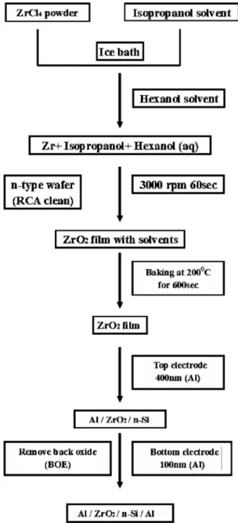
Figure 1 displays the main procedures used for sample prepara-tion. ZrO2 thin films were prepared using a sol-gel spin-coating method. ZrCl4共99.5%, Aldrich, USA兲 was used as the precursor for the synthesis of zirconia. Prior to film fabrication, the purity of ZrCl4was monitored using inductivity coupled plasma optical emis-*Electrochemical Society Active Member.
z
E-mail: fhko@mail.nctu.edu.tw
Journal of The Electrochemical Society, 153共6兲 F94-F99 共2006兲
0013-4651/2006/153共6兲/F94/6/$20.00 © The Electrochemical Society F94
sion spectrometry; apart from the signal for Zr, all other impurities were present at concentrations lower than 1000 ppm. The thin films were prepared through polymerization in an organic solution. A mother sol solution was first prepared by dissolving ZrCl4in isopro-panol共IPA; Fluka; water content ⬍0.1%兲 and hexanol 共Fluka; water content⬍5%兲 under vigorous stirring in an ice bath. The sol solu-tions were obtained after fully hydrolyzing ZrCl4 with a stoichio-metric quantity of water in IPA and hexanol to yield Zr/IPA/hexanol mixtures with molar ratios of 1:500:1000, 1:500:750, 1:500:500, and 1:500:250. The metal halide solution was then subjected to ultra-sonication at 0°C for 20 min to accelerate the gelling rate. The film thickness was determined using the ellipsometer. Film analyses 共AFM, ESCA, XRD, TDS-APIMS, TEM, C–V, and J–V兲 were con-ducted using the sample having a Zr IPA hexanol molar ratio of 1:500:1000.
The n-type wafers 共10–15 ⍀ cm, made in Japan兲, which were used as substrates for the metal insulator semiconductor 共MIS兲 structure, were RCA-cleaned to remove the native silicon oxide. ZrO2films were deposited by spin-coating at 3000 rpm for 60 s at ambient temperature共25°C兲 to give a thickness of ca. 9.3 nm on the
Figure 1. The sol-gel process used for the preparation of ZrO2films.
Figure 2. Cross-sectional TEM images of sol-gel-derived 共Zr + IPA
+ hexanol兲 ZrO2/Si structures annealed under an O2atmosphere at共a兲 200, 共b兲 600, and 共c兲 900°C.
n-Si共100兲 substrate. The spin-coater used was a TEL Clean Track model-MK8共Japan兲. These films were initially baked at 200°C for 10 min. One of the samples was then maintained at 200°C for 1 min for densification; the others were subjected to rapid thermal anneal-ing共RTA兲 at different temperatures 共500, 600, or 900°C兲 for 1 min under an oxygen atmosphere. ZrO2/n-Si structures were used in our experiments for the physical characterization of the zirconia.
Next, Al top electrodes having an area of 7.85⫻ 10−5cm2were deposited onto the top surface of the ZrO2by using a shadow mask and vaporizing a pure Al target. The thickness of the top electrode was 400 nm. A buffered oxide etch共BOE兲 was performed to remove the silicon back oxide and then the sample was thoroughly rinsed with deionized water. Finally, bottom electrodes were attached on the reverse side of the n-Si共100兲 substrates by vaporizing a pure Al target. The thickness of the bottom electrode was 100 nm. The di-electric properties were then determined for the MIS capacitors hav-ing an Al/ZrO2/n-Si/Al structure. This deposition technique allows the production of ultrathin gate dielectric films under excellent thickness control.
Results and Discussion
We studied the thicknesses of the smooth ZrO2films as a func-tion of the Zr/hexanol ratios. In this sol-gel process, the IPA solvent was more hydrophilic than hexanol. For this reason, we fixed the mole ratio of the IPA solvent with respect to the Zr ions at 1:500 共ZrCl4/IPA兲. We varied the hexanol content to provide various film thicknesses. The film thickness increased linearly upon decreas-ing the Zr/hexanol ratio from 1:1000 to 1:750 to 1:500 to 1:250. We obtained a smooth nanofilm共thickness 9.3 nm兲 at a Zr/hexanol ratio of 0.001. Prior to annealing, the real thicknesses of the smooth films obtained at Zr/hexanol ratios of 1:750, 1:500, and 1:250 were 10.7, 12.6, and 22.5 nm, respectively. The semi empirical linear fit between the thickness and the Zr/hexanol ratio关thickness
T共nm兲 = 4.55 + 4425.90⫻ 共Zr/hexanol兲 共correlation coefficient: R2= 0.9919兲兴 suggests that the film thickness is controllable and tunable by altering the Zr/hexanol ratio.
Figure 2a-c displays cross-sectional TEM images of the inter-faces of the ZrO2/Si structures annealed at 200, 600, and 900°C, respectively. The TEM image and its diffraction pattern in Fig. 2a indicate that the sol-gel-deposited film consists of a ca. 0.82-nm interfacial layer and a 9.3-nm-thick bulk ZrO2film, and the diffrac-tion pattern suggested that the ZrO2exhibited an amorphous struc-ture. Yamaguchi et al.9 observed the formation of an interfacial Zr-silicate layer after the pulsed-laser-ablation deposition of ZrO2. Wang and co-workers11 also proposed the presence of a Zr-silicate layer after atomic layer chemical vapor deposition of ZrCl4. We suggest that the interfacial layer in Fig. 2a may be attributed to such
a Zr-silicate. Very smooth interfaces exist in this sample. When we increased the annealing temperature to 600 and 900°C共Fig. 2b and c兲, the interfaces were also smooth and the ZrO2 films remained amorphous in structure, as judged from the diffraction pattern.
We used AFM to evaluate the surface quality of these sol-gel-derived zirconia films. The as-deposited共200°C兲 sample possessed a whole-area-film root-mean-square 共rms兲 roughness of 0.306 nm. After annealing at 500, 600, and 900°C under ambient oxygen for 1 min, the rms roughnesses were 0.157, 0.165, and 0.189 nm, re-spectively. The value of the surface roughness of the as-deposited ultrathin film after spin-coating was very low, and these films be-came even smoother after the annealing treatment. We determined the roughness of each sample at five different regions and found that the annealed samples remained smooth.
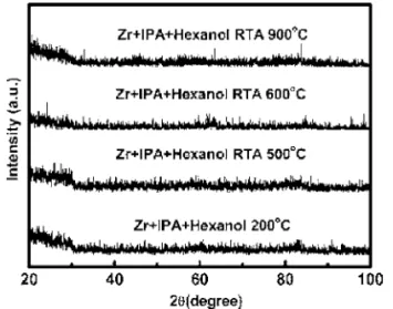
Next we investigated the ZrO2crystallinity using 1.5° glancing-angle XRD. High-k dielectric crystallinity is a concern because of possible problems arising from leakage paths and dopant/impurity diffusion along grain boundaries, as well as for the control of device uniformity. Figure 3 displays the XRD patterns of the ZrO2 films. Broad features are present in the XRD pattern of the as-deposited film; they did not change their appearance significantly after anneal-ing at temperatures up to 900°C. These results suggest that the samples have high thermal stability and that RTA treatment at 900°C for 1 min under an oxygen atmosphere does not result in the crystallization of ZrO2.
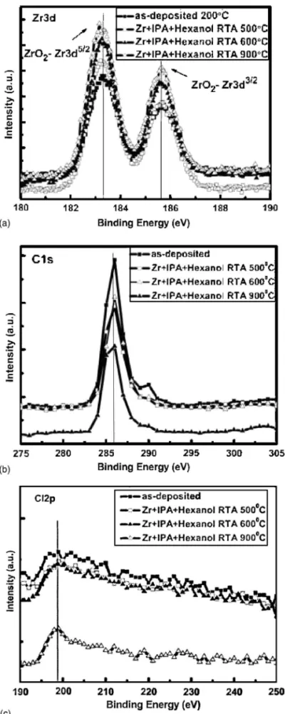
To determine the bulk properties of the deposited films, we used ESCA to examine the nature of the chemical bonding structures of these films. From the Zr 3d spectrum of the RTA samples in Fig. 4a, we observed clearly two typical peaks, Zr 3d5/2共183.2 eV兲 and Zr 3d3/2共185.6 eV兲, of ZrO2. RTA annealing under O2at 500, 600, and 900°C for 1 min led to remarkable changes in the ESCA spectra 共Fig. 4a兲. The intensities of the signals at 183.2 eV after annealing the as-deposited film at 500, 600, and 900°C were 1.24, 1.32, and 1.48 times higher, respectively, than that after baking at 200°C; similarly, the peak intensities at185.6 eV were 1.25, 1.38, and 1.54 times higher, respectively. That is to say, increases in the signals of the Zr–O bonds occur upon increasing the annealing temperature. As-deposited zirconia films exist mainly in the form ZrO2−␦ 共␦ ⬎ 0兲. Annealing under ambient oxygen can decrease the value of ␦, leading to the formation of ZrO2.8The electron binding energy of the C 1s orbital is 284 eV; this value increases to 286.5 eV when Cl is bound to C, as in Fig. 4b.20The C and Cl atoms both arise from the precursor or the solvents used during the preparation procedure. Annealing at 900°C in the oxygen-rich environment effectively re-duces the intensity of the C–Cl signal 共cf. Fig. 4b and c兲. This observation suggests that annealing is beneficial for enhancing the film’s quality and improving its electrical properties.
For ESCA analysis, the surfaces of these samples were sputtered away using a 2-kV argon beam 共scanning X-ray microprobe, Quantera SXM, ULVAC兲. Each sample was then eroded ⬃7 nm from the surface. In the spectrum of each RTA sample共Fig. 5兲, Si 2p peaks appears at 103.3 and 99.3 eV, corresponding to the binding energies of SiO2and Si–Si bonds, respectively.8It is obvious that the latter signal represents the silicon substrate. We found that the intensity of the peak representing the Si–O bonds in the annealed thin films increased upon increasing the annealing temperature共Fig. 5兲. This finding is consistent with our observations above regarding the TEM images共Fig. 2兲. The color at the interface region 共ZrO2/Si兲 lightened upon increasing the annealing temperature. This finding suggests that the Zr silicate at the interface led to phase separation at 900°C to form amorphous SiO2.8
As we mentioned above, C–Cl bonds existed in the ZrO2films; annealing at 900°C in the oxygen-rich environment significantly reduced their abundance. To verify this observation, we analyzed these samples through TDS-APIMS measurements. We ramped the desorption temperature of the TDS-APIMS system from room tem-perature to 800°C at 20°C/min under a N2carrier gas. We analyzed the surface out-gasses at molecular weights of 16, 44, and 82共Fig.
Figure 3. XRD data for ZrO2 films prepared under different conditions
共as-deposited and after annealing at the temperatures indicated兲.
F96 Journal of The Electrochemical Society, 153共6兲 F94-F99 共2006兲
6a-c兲. The film basically comprises Zr, Cl, C, H, and O elements derived from the preparation solvents and the precursor. The out-gassing molecular weights of 16 and 44 possibly represent carbon
elements in the forms CH4 and CO2, respectively. In addition, the chlorine components of the film combined with C atoms to form CCl2. We find that the organic elements of all of the samples dissi-pated violently at temperatures of ca. 400°C. As the annealing tem-perature increased, the intensity of the TDS-APIMS desorption peak gradually reduced. This result suggests that oxygen treatment at higher temperatures is beneficial for the separation of unstable carbon-containing compounds from the sol-gel-fabricated ultrathin film.
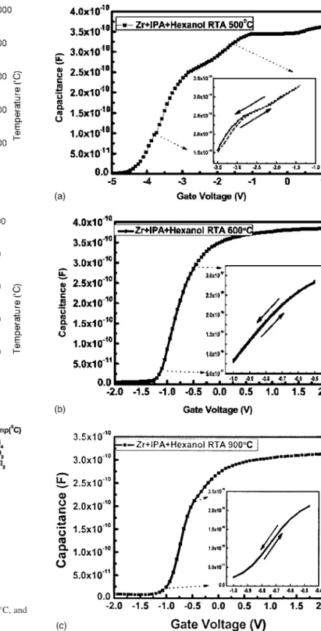
Figure 7 illustrates the high-frequency共1-MHz兲 capacitance vs gate voltage characteristics 共C–V curves兲 for the MIS capacitors prepared from sol-gel-derived ZrO2dielectrics under various anneal-ing conditions. For a high-k dielectric material, high-frequency C–V characteristics are important for calculating the equivalent oxide thickness共EOT兲. From Fig. 7a, we find that the shape of the C–V curve of the sample annealed at 500°C is poor; several steps exist in the curve, which is not very stable. In other words, the sample annealed at 500°C does not appear to have excellent electrical prop-erties because of the presence of unstable organic compounds re-maining in the film. This observation is consistent with our finding in Fig. 4b and 6a. When we raised the annealing temperature, the ZrO2 films exhibited good electrical properties, i.e., lower current densities and improved capacitance. Figure 7b provides detailed in-formation regarding the sample annealed at 600°C. The value of the capacitance of the RTA 600°C sample was 390 pF; this capacitor appears to be very stable. Table I lists the C–V characteristics of the RTA 600°C sample, which has an EOT value of 3.04 nm and a dielectric constant of 13.9. In addition, Fig. 7b displays hysteresis in the C–V characteristics of the samples in the absence of light. The solid line represents the C–V characteristics after measuring the curve by sweeping the voltage from accumulation to inversion and sweeping back共from +2.0 to −2.0 to +2.0 V兲; we observe that the shift is only 35 mV. We attribute this small shift to the reduction of unstable carbon-containing compounds after annealing.
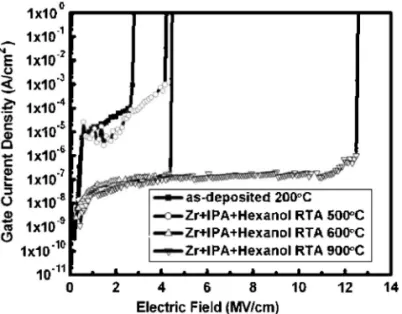
The capacitance of the film annealed at 900°C under an O2 at-mosphere was 310 pF共Fig. 7c兲. Thus, the capacitance of the RTA 900°C sample was lower than that of the RTA 600°C sample. From the ESCA signals of these samples, we find that the intensity of the peak for the Si–O bonds in the annealed thin film increased upon increasing the annealing temperature 共see Fig. 5兲. The interfacial oxide共SiO2兲 influences the capacitance and the EOT, which is an undesirable property. Nevertheless, the sol-gel-derived ZrO2 films annealed at 900°C display 共Fig. 8兲 an improved breakdown field 共⬎12 MV/cm2兲. Table I lists the C–V characteristics of the sample
Figure 4. 共a兲 ESCA spectra of as-deposited ZrO2films and after RTA
an-nealing at 500, 600, and 900°C in O2for 1 min共Zr 3d兲. ESCA spectra of 共b兲 Cl and共c兲 C atoms after annealing at different temperatures.
Figure 5. ESCA spectra共Si 2p兲 of ZrO2films eroded by ca. 7 nm using an
annealed at 900°C; the value of EOT was 3.91 nm and the dielectric constant was 12.8. We observe that as the annealing temperature increased, the EOT increased共from 3.07 to 3.91 nm兲 and the dielec-tric constant decreased共from 13.9 to 12.8兲. The solid line in the inset of Fig. 7c represents the C–V characteristics after measuring the curve by sweeping the voltage from accumulation to inversion and sweeping back共from +2.0 to −2.0 to +2.0 V兲. We observe a shift of 20 mV for the hysteresis phenomenon for the sample an-nealed at 900°C. Thus, the hysteresis phenomenon is lower than the dielectrics of the sol-gel-derived ZrO2film annealed at 600°C.
We obtained the electric field共E兲 in the J–E curve of Fig. 8 by using the equation E = V/tox, where V is the applied voltage and tox is the EOT determined through C–V measurement. The samples
annealed at 200 and 500°C did not have sufficiently high thermal budgets and thus, their breakdown electric fields were relatively low. The breakdown electric fields increased upon increasing the anneal-ing temperature. A high annealanneal-ing temperature removed unstable carbon-containing compounds from the ZrO2film and stabilized the thin film. The sol-gel-derived ZrO2films displayed excellent electri-cal performances because they did not crystallize during high-temperature RTA, even after annealing at high-temperatures as high as 900°C. In addition, the samples subjected to RTA treatment at 600
Figure 6. TDS-APIMS analyses of the共a兲 RTA 500°C, 共b兲 RTA 600°C, and
共c兲 RTA 900°C samples.
Figure 7. High-frequency 共1 MHz兲 C–V characteristics of the
sol-gel-derived ZrO2dielectrics after RTA at共a兲 500, 共b兲 600, and 共c兲 900°C under an O2atmosphere.
F98 Journal of The Electrochemical Society, 153共6兲 F94-F99 共2006兲
and 900°C displayed leakage current densities 共⬍10−7A/cm2兲 lower than those reported in the literature for amorphous ZrO2 films.8,11
Thin layers of zirconium dioxide that are used as dielectrics for capacitors or as gate oxides for MIS devices are subject to a mechanism known as time-dependent dielectric breakdown 共TDDB兲. This mechanism causes the dielectric to break down and electrically short after a certain duration of operation. The expected lifetime of a thin gate oxide under normal operating conditions should be several million years. Figure 9 displays a projected life-time operation of ca. 1.1 MV/cm for the Zr + IPA + hexanol RTA 500°C sample 共five replicate measurements for each point兲. The projected lifetime operation of the Zr + IPA + hexanol RTA 600°C sample is ca. 2.1 MV/cm, and that of the Zr + IPA + hexanol RTA 900°C sample is ca. 10.4 MV/cm. In this figure, we observe a large increment in the projection voltage for the 10-year lifetime when the Zr + IPA + hexanol sample was annealed at 900°C. This result oc-curs because the high annealing temperature stabilizes the ZrO2 film.
Conclusions
In this paper, we propose a sol-gel method for preparing ultrathin films that is attractive because of its low cost and because of the improved thermal and electrical properties of the films. The sol-gel method requires a lower degree of processing and provides highly homogeneous materials; the possibility exists to use annealing pro-cesses to stabilize the film. We prepared ZrO2 ultrathin films of amorphous phase through sol-gel processing using ZrCl4 as the metal halide. The ZrO2thin films not only display good electrical insulation 共breakdown fields of up to 12.5 MV/cm兲 but also im-proved thermal stability against crystallization共up to 900°C兲. These
ZrO2 ultrathin films, which are readily produced, may behave as suitable capacitors and coatings for insulating films.
Acknowledgment
This study was supported financially by the National Science Council, Taiwan, ROC, through contract no. NSC 94-2113-M-009-020.
National Chiao Tung University assisted in meeting the publication costs of this article.
References
1. Y. Ma, Y. Ono, L. Stecker, D. R. Evans, and S. T. Hsu, Tech. Dig. - Int. Electron
Devices Meet., 1999, 149.
2. W. J. Qi, R. Nieh, B. H. Lee, L. Kang, Y. Jeon, K. Onishi, T. Ngai, S. Banerjee, and J. C. Lee, Tech. Dig. - Int. Electron Devices Meet., 1999, 145.
3. R. E. Nieh, C. S. Kang, H. J. Cho, K. Onishi, R. Choi, S. Krishnan, J. H. Han, Y. H. Kim, M. S. Akbar, and J. C. Lee, IEEE Trans. Electron Devices, ED-50, 333 共2003兲.
4. C. H. Lee, H. F. Luan, W. P. Bai, S. J. Lee, T. S. Jeon, Y. Senzaki, D. Roberts, and D. L. Kwong, Tech. Dig. - Int. Electron Devices Meet., 2000, 27.
5. W. J. Qi, R. Nieh, B. H. Lee, K. Onishi, L. Kang, Y. Jeon, J. C. Lee, V. Kaushik, B. Y. Neuyen, L. Prabhu, K. Eisenbeiser, and J. Finder, VLSI Technical Digest, p. 40共2000兲.
6. T. Yamaguchi, H. Satake, and N. Fukushima, Tech. Dig. - Int. Electron Devices
Meet., 2001, 663.
7. Z. J. Luo, T. P. Ma, E. Cartier, M. Copel, T. Tamagawa, and B. Halpern, VLSI
Technical Digest, p. 135共2001兲.
8. J. Zhu, Z. G. Liu, M. Zhu, G. L. Yuan, and J. M. Liu, Appl. Phys. A: Mater. Sci.
Process., 80, 321共2005兲.
9. T. Yamaguchi, H. Satake, N. Fukushima, and A. Toriumi, Tech. Dig. - Int. Electron
Devices Meet., 2000, 19.
10. Y. Kim, G. Gebara, M. Freiler, J. Barneet, D. Riely, J. Chen, K. Torres, J. Lim, B. Foran, F. Shappur, A. Agarwal, P. Lysaght, G. A. Brown, C. Young, S. Borthakur, H. J. Li, B. Nguyen, P. Zeitzoff, G. Bersuker, D. Derro, R. Bergmann, R. W. Murto, A. Hou, H. R. Huff, E. Shero, C. Pomarede, M. Givens, M. Mazanec, and C. Werkhoven, Tech. Dig. - Int. Electron Devices Meet., 2001, 455.
11. J. C. Wang, S. H. Chiao, C. L. Lee, T. F. Lei, Y. M. Lin, M. F. Wang, S. C. Chen, C. H. Yu, and M. S. Liang, J. Appl. Phys., 92, 3936共2002兲.
12. J. P. Chang, Y. S. Lin, and K. Chu, J. Vac. Sci. Technol. B, 19, 1782共2001兲. 13. J. P. Chang and Y. S. Lin, J. Appl. Phys., 90, 2964共2001兲.
14. R. Caruso, A. D. Parralejo, P. Miranda, and F. Guiberteau, J. Mater. Res., 16, 2391 共2001兲.
15. K. T. Miller and F. F. Lange, J. Mater. Res., 6, 2387共1991兲.
16. E. S. González, P. Miranda, A. D. Parralejo, A. Pajares, and F. Guiberteau, J.
Mater. Res., 20, 1544共2005兲.
17. V. Kiisk, I. Sildos, S. Lange, V. Reedo, T. Tätte, M. Kirm, and J. Aarik, Appl. Surf.
Sci. 247, 412共2005兲.
18. C. J. Brinker and G. W. Scherer, Sol-Gel Science, Academic Press, New York 共1989兲.
19. A. J. Moulson and J. M. Herbert, Electroceramics, Wiley, New York共2003兲. 20. J. C. Vickerman, Surface Analysis, Wiley, New York共1997兲.
Table I. Properties of films annealed at 600 and 900°C.
Heat-treatment condition Dielectric constant共k兲 EOT共nm兲 Zr + IPA + hexanol, RTA 600°C, 1 min 13.9 3.04 Zr + IPA + hexanol, RTA 900°C, 1 min 12.8 3.91
Figure 8. Gate current density vs electric field共J–E兲 characteristics of the
ultrathin film after RTA treatment. Figure 9. TDDB lifetime projections for the Zr + IPA + hexanol samples after RTA at 500, 600, and 900°C, respectively.