Optical properties of a -plane InGaN/GaN multiple quantum wells on r -plane sapphire
substrates with different indium compositions
C. H. Chiu, S. Y. Kuo, M. H. Lo, C. C. Ke, T. C. Wang, Y. T. Lee, H. C. Kuo, T. C. Lu, and S. C. Wang
Citation: Journal of Applied Physics 105, 063105 (2009); doi: 10.1063/1.3083074
View online: http://dx.doi.org/10.1063/1.3083074
View Table of Contents: http://scitation.aip.org/content/aip/journal/jap/105/6?ver=pdfcov Published by the AIP Publishing
Articles you may be interested in
The defect character of GaN growth on r -plane sapphire J. Appl. Phys. 107, 073525 (2010); 10.1063/1.3369439
Exciton localization on basal stacking faults in a -plane epitaxial lateral overgrown GaN grown by hydride vapor phase epitaxy
J. Appl. Phys. 105, 043102 (2009); 10.1063/1.3075596
Improved a -plane GaN quality grown with flow modulation epitaxy and epitaxial lateral overgrowth on r -plane sapphire substrate
Appl. Phys. Lett. 92, 231902 (2008); 10.1063/1.2942391
Erratum: “Interfacial structure of a -plane GaN grown on r -plane sapphire” [Appl. Phys. Lett.90, 081918 (2007)] Appl. Phys. Lett. 90, 249901 (2007); 10.1063/1.2744473
Interfacial structure of a -plane GaN grown on r -plane sapphire Appl. Phys. Lett. 90, 081918 (2007); 10.1063/1.2696309
Optical properties of a-plane InGaN/GaN multiple quantum wells on r-plane
sapphire substrates with different indium compositions
C. H. Chiu,1,a兲 S. Y. Kuo,2 M. H. Lo,1C. C. Ke,1T. C. Wang,1 Y. T. Lee,1 H. C. Kuo,1,a兲 T. C. Lu,1and S. C. Wang1
1
Department of Photonics and Institute of Electro-Optical Engineering, National Chiao-Tung University, Hsinchu, Taiwan, Republic of China
2Department of Electronic Engineering, Chang Gung University, TaoYuan, Taiwan, Republic of China 共Received 6 October 2008; accepted 14 January 2009; published online 24 March 2009兲
A-plane InxGa1−xN/GaN 共x=0.09, 0.14, 0.24, and 0.3兲 multiple-quantum-wells 共MQWs兲 samples, with a well width of about 4.5 nm, were achieved by utilizing r-plane sapphire substrates. Optical quality was investigated by means of photoluminescence 共PL兲, cathodoluminescence, and time resolved PL measurements共TRPL兲. Two distinguishable emission peaks were examined from the low temperature PL spectra, where the high- and low-energy peaks were ascribed to quantum wells and localized states, respectively. Due to an increase in the localized energy states and absence of quantum confined Stark effect, the quantum efficiency was increased with increasing indium composition up to 24%. As the indium composition reached 30%, however, pronounced deterioration in luminescence efficiency was observed. The phenomenon could be attributed to the high defect densities in the MQWs resulted from the increased accumulation of strain between the InGaN well and GaN barrier. This argument was verified from the much shorter carrier lifetime at
15 K and smaller activation energy for In0.3Ga0.7N/GaN MQWs. In addition, the
polarization-dependent PL revealed that the degree of polarization decreased with increasing indium compositions because of the enhancement of zero-dimensional nature of the localizing centers. Our detailed investigations indicate that the indium content in a-plane InGaN/GaN MQWs not only has an influence on optical performance, but is also important for further application of nitride semiconductors. © 2009 American Institute of Physics.关DOI:10.1063/1.3083074兴
I. INTRODUCTION
InGaN-based semiconductors have been used intensively as light emitting diodes共LEDs兲 and laser diodes due to their wide direct band gap ranging from green to ultraviolet light.1 However, the quantum efficiency is limited in the conven-tional c-plane polar structure due to the built-in electric field called quantum confined Stark effect 共QCSE兲. This built-in electric field would decrease the oscillator strength of the electron-hole pairs and reduce the carrier recombination rate. Thus in highly efficient InGaN/GaN multiple quantum wells 共MQWs兲 based devices, the InGaN well has a thickness of less than 3 nm to avoid degradation of the light emission by the QCSE. Moreover, because of the low miscibility of InN in GaN, there exists partial phase segregation within InGaN-based structures.2This partial phase segregation and compo-sition inhomogeneity would result in exciton localization within some indium-rich regions.3 Consequently, the lumi-nescence efficiency could be enhanced due to the effective carrier confinement in the localization states. Such exciton localization effect is influenced by the quantum well thick-ness, indium compositions, and doping concentration. For
c-plane InGaN/GaN MQWs, the influence of indium
compo-sitions on the optical characteristics has been studied exten-sively in order to optimize InGaN/GaN MQW quantum efficiency.4,5
Recently, several groups have grown samples with non-polar structures in order to eliminate the built-in electric field.6Our group also reported the influence on optical prop-erties of a-plane In0.23Ga0.77N MQWs with different well width ranging from 3 to 12 nm and we found the photolumi-nescence共PL兲 intensity decreased as the well width was in-creased especially for those larger than⬃6–7 nm.7 Nonpo-lar InGaN/GaN MQWs containing less indium can be used to extend the light emission to the green spectral range due to the absence of QCSE, which is still a challenge for high efficiency InGaN/GaN MQW LEDs and lasers. Up to now, however, the structural and optical properties of nonpolar InGaN/GaN MQWs are still inferior compared to their ma-ture c-plane grown counterpart due to much higher disloca-tion densities when grown on r-plane sapphire substrates.
In this paper, the optical properties of the a-plane关112¯0兴 InxGa1−xN/GaN MQWs on r-plane sapphire substrates with different indium compositions共x⬃9%, 14%, 24%, and 30% with well width of ⬃4.5 nm兲 have been investigated by means of PL, cathodoluminescence共CL兲, and time resolved PL measurements共TRPL兲. The influence of indium compo-sition on luminescence efficiency in InGaN/GaN MQWs as well as polarization properties is discussed.
II. EXPERIMENT
The 1.5-m-thick a-plane 关112¯0兴 bulk GaN was grown by Aixtron 2400G3 multiwafer low pressure metal-organic chemical vapor deposition 共LP-MOCVD兲 on r-plane sap-a兲Authors to whom correspondence should be addressed. Electronic
ad-dresses: [email protected] and [email protected].
0021-8979/2009/105共6兲/063105/6/$25.00 105, 063105-1 © 2009 American Institute of Physics
phire substrates using conventional two-step growth technique.8 Four samples with identical structure and 10 pairs of 4.5-nm-thick InGaN well/18-nm-thick GaN barrier MQWs were under the same growth condition except for the growth temperature. The growth temperature for the four samples was controlled at 870, 850, 830, and 810 ° C, re-spectively. The anisotropic strain within nonpolar structures will result in more complex Poisson ratio. After high reso-lution x-ray diffraction measurements, we could estimate the indium compositions to be ⬃9%, 14%, 24%, and 30% for
InGaN/GaN MQW samples.9
III. RESULTS AND DISCUSSIONS
First, the power-dependent PL measurement of the four samples at room temperature was performed as shown in Fig.1共a兲. All samples were excited by a 325 nm He–Cd laser with an excitation power of 35 mW and the emitted lumines-cence light was collected through a 0.32 m spectrometer with a charge-coupled device detector. The focused spot size of the laser was estimated to be about 200 m in diameter. As illustrated in Fig.1共a兲, the room-temperature PL peak emis-sion energy of InGaN/GaN MQWs decreases from 2.89 to
2.36 eV through all samples despite various excitation power. Furthermore, all samples show extremely small shift in emission peak energy with increasing the pumping power from 0.4 to 35 mW. The integrated PL intensity was fitted based on the relation I⬃ P␣, where I is the integrated PL intensity, P is the excitation power density, and ␣ is the power index. Shown in Fig. 1共b兲 are the fitting results of integrated PL intensity. While increasing indium composition from 9% to 30%, the␣factors of the four samples were 1.04, 1.08, 1.04, and 1.01, respectively. From the negligible PL peak emission energy shift and nearly identical ␣factors, it is suggested that the QCSE is extremely small or absent in our a-plane InGaN/GaN MQWs with indium compositions varying from⬃9% to 30%.
Figure 2 shows the temperature-dependent PL spectra taken from 20 to 300 K at an excitation power of 30 mW. At low temperature, the spectra exhibit a multiple-peak feature and can be decomposed into two dominant peaks, higher-energy emission共denoted by PH兲 and lower-energy emission
共denoted by PL兲. As the temperature increases, the peak
in-tensity of PH quenches quickly and the PL becomes
domi-nant for all InGaN/GaN MQW samples. It is suggested that
PH is a MQW-related emission and PL is from the deep
localized states. This argument will be discussed by TRPL results later.
To further clarify the PL mechanism, the 20 K PL spec-tra were decomposed into a sum of two Gaussian curves, PH
and PL, mentioned above. Fitting results are shown in Figs.
3共a兲and3共b兲 for four InGaN/GaN MQWs samples. In Fig.
3共a兲, we can clearly see that both emission peak energies decreased as the indium concentration increased. On the other hand, the peak emission difference seems to be gradu-ally increased from 240 to 290 meV. The difference between these two emission peaks suggests that the higher the indium compositions, the deeper the localized centers existing in InGaN/GaN MQWs. Thus the carrier would be easier to mi-grate to the lowest state in the high indium concentration sample. This phenomenon could explain the enhanced peak intensity ratio of the PLto PHpeaks as indium concentration
increased. Figure 3共b兲 summarizes the full width at half maximum共FWHM兲 of these two peaks for all samples at 20 K. It is noteworthy that the FWHM of the PLpeaks keeps
constant in all samples while that of the PH peak increases
linearly with indium compositions. This broadening phenom-enon of the PL peak indicates that an increasing degree of
compositional and structural disorders with increasing in-dium concentration deteriorates the crystal quality in the quantum wells, which has been extensively reported.
In addition, the evolution with temperature of the peak shift of PL peak for the four samples investigated here is
given in Fig.3共c兲, where the peak positions at 20 K are the reference. The peak shift of PL varies as a function of tem-perature from 20 to 300 K and exhibits a continuous redshift. With increasing indium composition, the total redshift value at room temperature in Fig.3共c兲reduced from 85 to 30 meV. The smaller redshift may be due to more localization centers with higher indium compositions.10Thus the confinement of the localization would be improved as we increase indium composition, which is consistent with the result of Fig.3共c兲.
0 5 10 15 20 25 30 35 40 2.3 2.4 2.5 2.6 2.7 2.8 2.9 3.0 x=0.30 x=0.24 x=0.14 PL P eak Energy (eV ) Excitation Power (mW) In xGa1-xN/GaN x=0.09 (a) 0 100 200 300 400 αα=1.04 αα=1.01 αα=1.08 InxGa1-xN/GaN x=0.09 x=0.14 x=0.24 x=0.3
Intensity
(a.u.)
Power density (mW/cm2) αα=1.04 (b)FIG. 1. 共Color online兲 The power-dependent PL measurement of the four samples,共a兲 the emission wavelength vs the pumping power and 共b兲 the PL intensity vs the pumping density and fitted based on the relation I⬃ P␣.
063105-2 Chiu et al. J. Appl. Phys. 105, 063105共2009兲
It has been studied that the carrier could receive activa-tion energy to thermalize from the potential minima, the ra-diative or localized centers, to nonrara-diative or delocalized centers as the temperature is increased.11Therefore, it is ex-pected that the deeper localization with better confinement should have larger activation energy. In order to further verify that, the experimental temperature-dependent PL data were fitted by Arrhenius equation to investigate the carrier behavior during the thermal processes,12
I共T兲 = IO 1 + Aⴱexp
冉
− Ea KBT冊
+ Bⴱexp冉
− Eb KBT冊
,where I共T兲 is the temperature-dependent PL intensity, I0 is the PL intensity at 20 K, KBis Boltzmann’s constant, A and
B are the rate constants, and Ea and Eb are the activation
energies for two different nonradiative channels, which can be distinguished for the low temperature and high tempera-ture regions.13 The fitted activation energy of the four samples is listed in Fig.4. As expected, the activation energy gradually increases and reaches the maximum value of 110 meV when indium composition is 24%. It has been reported that several defects such as V-defects, stacking faults, and dislocations will be formed in the MQWs during sample growth, resulting in deterioration in the structural and optical properties of MQWs.14Consequently, as indium composition is continuously increased, large numbers of defects may exist in our samples. Photogenerated carriers will be easily trapped by high-density nonradiative centers before they reached the potential minimum. Thus the activation energy
) 2.2 2.4 2.6 2.8 3.0 3.2 3.4 N o rm al ize d P L Inten is ty (a rb . u nits) Energy(eV) 20 40 60 80 90 100 110 120 130 140 160 180 200 220 240 260 280 300 InxGa1-xN/GaN x=0.14 . u nits ity(a Intens liz Norma 2.2 2.4 2.6 2.8 3.0 3.2 3.4 PL ed PL rb Energy(eV) 20 40 60 80 90 100 110 120 130 140 160 180 200 220 240 260 280 300 InxGa1-xN/GaN x=0.09 PH
(a)
(b)
) rb. u n n sity PL Int a lize No 2.2 2.4 2.6 2.8 3.0 3.2 3.4 2.2 2.4 2.6 2.8 3.0 3.2 3.4 N o rm alize d PL In ten s ity (arb . u n its) Energy(eV) 20 40 60 80 100 110 120 130 140 160 180 200 220 240 260 280 300 InxGa1-xN/GaN x=0.30 rm d e (a its Energy(eV) 20 40 60 80 90 100 110 120 130 140 160 180 200 220 240 260 280 300 InxGa1-xN/GaN x=0.24(c)
(d)
FIG. 2.共Color online兲 The PL emission spectra under temperature varied from 1 to 300 K. 共a兲 –共d兲 imply the samples with In compositions varied from 9% to 30%.
of InGaN/GaN MWQs with 30% indium composition low-ered to 85 meV.
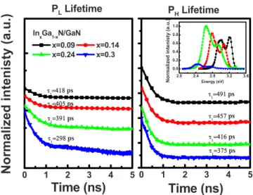
Furthermore, the TRPL measurements at 15 K were per-formed to investigate the effects of indium compositions on the carrier recombination mechanism as shown in Fig.5. The experimental data exhibit a nonexponential called stretched exponential decay shape, which is a characteristic of the emission from disorder quantum structures such as the local-ized states.15,16 The TRPL results can be fitted by the stretched exponential decay shape,
I共t兲 = I1共0兲exp
冉
− t 1冊
+ I2共0兲exp冉
−冉
t 2冊
冊
,where I共t兲 is the PL intensity at time t, is the dimension-ality of the localized centers, and 1 and 2 represent the initial lifetimes of the carriers. Normally, the fast decay term 1 is used represent PL since the PL intensity is limited by the fast decay component,17 so we labeled all fitted1 near the curves. From Fig.5, we found that the fitted lifetime of 1equals 418, 405, 391, and 289 ps in PLand 491, 457, 416,
and 375 ps in PHfor indium composition changing from 9%
to 30%. It first shows that the PLpeaks have shorter lifetime
than PHpeaks in all samples. The results of shorter lifetime
of PLcoincide with the stronger emission intensity than the PHshowing in the inset of Fig. 5, since it corresponds to a
higher recombination rate at low temperature. Therefore, it is reasonable to assign the PH and PL to MQWs-related and
localized states emission, respectively. Second, the carrier lifetime of PL slightly decreased as indium composition is
5 10 15 20 25 30 1.8 2.0 2.2 2.4 2.6 2.8 3.0 3.2 0.22 0.24 0.26 0.28 0.30 0.32 0.34 0.36 0.38 0.40 Peak at 15K P e ak energy (e V ) In composition (%) P L P H Emission difference (a) (b) 5 10 15 20 25 30 120 160 200 240 280 FHWM at 15K FWHM (meV) In composition (%) PL PH (c) 0 50 100 150 200 250 300 -80 -60 -40 -20 0 PL Peak S hi ft (meV ) Temperature (K) InxGa1-xN/GaN x=0.09 x=0.14 x=0.24 x=0.30
FIG. 3. 共Color online兲 The summary of the temperatudependent PL re-sults of the four samples with different In compositions.共a兲 shows the emis-sion wavelength and difference between high and low emisemis-sion peaks,共b兲 shows the FWHM of the dominate and high energy peaks, and共c兲 shows the dominate wavelength shift from 20 to 300 K.
0.00 0.01 0.02 0.03 0.04 0.05 Eb=85 meV Eb=110 meV Eb=95 meV
intensity
(a.u.
)
1/T (1/K)
InxGa1-xN/GaN x=0.09 x=0.14 x=0.24 x=0.3 Eb=89 meVFIG. 4.共Color online兲 The normalized PL intensity plotted as a function of 1/T for the samples with different In compositions. The symbols stand for the measurement results and the solid line means the fitted curve of the four samples. The number labeled near the curves represents the fitted activation energies. 2.0 2.4 2.8 3.2 3.6 0.0 0.2 0.4 0.6 0.8 1.0 Norm ali zed in ten ist y (a .u. ) Energy (eV) 0 1 2 3 4 5 0 1 2 3 4 5 PHLifetime ττ11=2=29898ps ττ11=3=39191ps ττ11=4=40505ps ττ11=4=41818ps In xGa1-xN/GaN x=0.09 x=0.14 x=0.24 x=0.3
Normalized
intenist
y
(a.u.
)
Time (ns)
PLLifetimeTime (ns)
ττ11=4=49191ps ττ11=4=45757ps ττ11==416416ps ττ11=3=37575psFIG. 5. 共Color online兲 The measured lifetime of PH and PL peaks for
samples with different In compositions at 15 K. The inset shows the mea-sured PL spectra of the four samples.
063105-4 Chiu et al. J. Appl. Phys. 105, 063105共2009兲
below 24%, but dropped from 391 to 289 ps as the indium composition increased from 24% to 30%. As expected, the integrated PL intensity is reversely proportional to the carrier lifetime as x is below 24%. However, contrary to our expec-tations, the PL intensity of the sample with 30% indium com-position drops to about only 1/5 compared to the lumines-cence intensity of the sample with 24% indium composition. It is known that the nonradiative lifetime is much shorter than radiative lifetime, so the appreciable reduction in life-time and PL intensity revealed the fact of large number of nonradiative centers in the sample with 30% indium composition.18 For the InGaN alloy system, nanoscale fluc-tuations in the local indium concentration are expected to form easily and produce more disorder. Therefore, the carrier recombination is probably determined by another nonradia-tive mechanism. Further evidence of indium phase segrega-tion by CL image mapping will be discussed later. In addi-tion, the lifetime extracted from the a-plane samples under 15 K is much shorter共⬍0.5 ns兲 than that of c-plane MQWs reported in previous literature关⬃5.8 ns 共Ref.6兲兴.
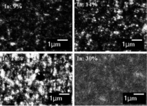
Taking luminescence efficiency into consideration, CL mapping measurement could provide constructive informa-tion. Figure6shows the CL images of the four samples with a JEOL-JSM 6500 scanning electron microscope under an accelerating voltage of 15 kV at room temperature. The four images were scanned at monitoring the respective peak emis-sion wavelength. At first glance, the nonuniform emisemis-sion patterns are observed from all samples, which were mainly due to the indium composition fluctuation and the phase separation.19 Interestingly, it is found that, with the increase in indium composition, the emission area and intensity gradually increase and, hence, exhibit a better uniformity emission pattern, except for the sample with highest indium compositions. It suggests that In0.24Ga0.76N/GaN MQWs sample has relatively higher luminescence efficiency among these samples.
In order to demonstrate the optical characteristic of non-polar MQWs, the non-polarization-dependent PL measurement was taken. Shown in Fig.7is the polarization ratio plotted as the function of indium compositions at 20 and 300 K. The degree of polarization 共DOP兲 is defined as DOP=I⬜− I储/I⬜ + I储, where I⬜ and I储are PL intensities represented for E⬜C and E储C. As we can see from Fig. 7, DOP decreased as temperature increased in all samples. This feature might be
explained that carriers in these samples have sufficient en-ergy to be thermally distributed to the other local minimums states. Accordingly, the DOP decreases with increasing temperature.20 In addition, DOP decreases with increasing indium composition. The decrease in the DOP might be at-tributed to the enhancement of zero-dimensional nature of the localizing radiative centers, most of which are the dotlike indium-rich region in MQWs. Therefore, with increasing in-dium compositions, more carriers would be confined at lo-calization centers which then reduces the DOP.21
IV. CONCLUSION
In summary, the optical properties of the samples grown by LP-MOCVD on r-plane sapphire with different indium compositions ranging from 9% to 30% were investigated. All samples manifest two distinguishable emission peaks, where the high-energy and low-energy peaks were attributed to quantum wells and localized states, respectively. No obvious emission peak shift is observed from the power-dependent PL measurement for all samples, which is the evidence to the absence of QCSE. While the indium composition was raised to 24%, the increase in activation energy and decrease in carrier lifetime implied that more and deeper localized states formed and contribute to better quantum efficiency. How-ever, the MQWs sample with 30% indium composition re-veals dramatic reduction in activation energy and lifetime at low temperature. The observation implied the large numbers of defects formed in high indium samples, consistent with earlier literatures. Besides, from the polarization-dependent PL measurement, the DOP reduced in increasing tempera-tures and indium compositions. The phenomenon might be related to the enhancement in zero-dimensional nature of the localized radiative centers. These results suggest that In0.24Ga0.76N/GaN MQWs sample has the relatively higher luminescence efficiency among these samples, which pro-vides useful guidance for the fabrication of high efficiency LEDs with a-plane InGaN/GaN MQW structures.
FIG. 6. Top view cathodoluminescence images of a-plane InGaN/GaN MQWs with different In compositions at corresponding dominate emission peak wavelengths. 5 10 15 20 25 30 35 20 30 40 50 60 70 80 Degree o f pola rization (%) In composition(%) 20K 300K
FIG. 7. 共Color online兲 The DOP plotted as the function of In compositions at 20 and 300 K, respectively.
ACKNOWLEDGMENTS
The authors thank Professor J. L. Shen of Chung Yuan Christian University for useful discussion. The work was supported by the MOE ATU program and in part by the National Science Council in Taiwan under Contract Nos. NSC 95-2120-M-009-008, NSC 95-2752-E-009-007-PAE, and NSC 95-2221-E-009-282, and Epistar Co. Ltd. in Taiwan.
1S. Nakamura and G. Fasol, The Blue Laser Diode共Springer, Berlin, 1997兲. 2I. Ho and G. B. Stringfellow,Appl. Phys. Lett.69, 2701共1996兲. 3R. W. Martin, P. G. Middleton, K. P. O’Donnell, and W. Van Der Stricht,
Appl. Phys. Lett.74, 263共1999兲.
4H. C. Yang, P. F. Kuo, T. L. Lin, Y. F. Chen, K. H. Chen, L. C. Chen, and
J.-I. Chyi,Appl. Phys. Lett.76, 3712共2000兲.
5A. Sasaki, S. I. Shibakawa, Y. Kawakami, K. Nishizuka, Y. Narukawa, and
T. Mukai,Jpn. J. Appl. Phys., Part 145, 8719共2006兲. InxGa1−xN/GaN. 6P. Waltereit, O. Brandt, A. Trampert, H. T. Grahn, J. Menniger, M.
Ram-steiner, M. Reiche, and K. H. Ploog,Nature共London兲406, 865共2000兲.
7T. S. Ko, T. C. Lu, T. C. Wang, M. H. Lo, J. R. Chen, R. C. Gao, H. C.
Kuo, and S. C. Wang,Appl. Phys. Lett.90, 181122共2007兲.
8T. C. Wang, T. S. Ko, T. C. Lu, H. C. Kuo, R. C. Gao, J. D. Tsay, and S.
C. Wang, Phys. Status Solidi 5,共c兲, 2161 共2008兲.
9S. Nakamura, G. Fasol, and S. J. Pearton, The Blue Laser Diode the
Complete Story, 2nd ed.共Springer, Berlin, 2000兲.
10S. F. Chichibu, T. Azuhata, T. Kitamura, Y. Ishida, H. Okumura, H.
Nakanishi, T. Sota, and T. Mukai,J. Vac. Sci. Technol. B19, 2177共2001兲.
11Y. H. Cho, G. H. Gainer, A. J. Fischer, J. J. Song, S. Keller, U. K. Mishra,
and S. P. DenBaars,Appl. Phys. Lett.73, 1370共1998兲.
12A. Yasan, R. McClintock, K. Mayes, D. H. Kim, P. Kung, and M. Razeghi,
Appl. Phys. Lett.83, 4083共2003兲.
13M. Leroux, N. Grandjean, B. Beaumont, G. Nataf, F. Semond, J. Massies,
and P. Gibart,J. Appl. Phys.86, 3721共1999兲.
14H. K. Cho, J. Y. Lee, C. S. Kim, and G. M. Yang,J. Electron. Mater.30,
1348共2001兲.
15X. Chen, B. Henderson, and K. P. O’Donnell,Appl. Phys. Lett.60, 2672
共1992兲.
16T. Onuma, T. Koyama, A. Chakraborty, M. Mclaurin, B. A. Haskell, P. T.
Fini, S. Keller, S. P. DenBaars, J. S. Speck, S. Nakamura, U. K. Mishra, T. Sota, and S. F. Chichibu,J. Vac. Sci. Technol. B25, 1524共2007兲.
17T. Onuma, A. Chakraborty, B. A. Haskell, S. Keller, S. P. DenBaars, J. S.
Speck, S. Nakamura, and U. K. Mishra, Appl. Phys. Lett.86, 151918 共2005兲.
18S. F. Chichibu, T. Onuma, T. Aoyama, K. Nakajima, P. Ahmet, T.
Chi-kyow, T. Sota, S. P. DenBaars, S. Nakamura, T. Kitamura, Y. Ishida, and H. Okumura,J. Vac. Sci. Technol. B21, 1856共2003兲.
19P. Waltereit, O. Brandt, M. Ramsteiner, A. Trampert, H. T. Grahn, J.
Menniger, M. Reiche, and K. H. Ploog, J. Cryst. Growth 227–228, 437 共2001兲.
20M. Kubota, K. Okamoto, T. Tanaka, and H. Ohta,Appl. Phys. Lett.92,
011920共2008兲.
21T. Koyama, T. Onuma, H. Masui, A. Chakraborty, B. A. Haskell, S.
Keller, U. K. Mishra, J. S. Speck, S. Nakamura, and S. P. DenBaars,Appl. Phys. Lett.89, 091906共2006兲.
063105-6 Chiu et al. J. Appl. Phys. 105, 063105共2009兲