against copper oxidation
Jui-Chang Chuang and Mao-Chieh Chen
Citation: Journal of Vacuum Science & Technology B 16, 3021 (1998); doi: 10.1116/1.590336
View online: http://dx.doi.org/10.1116/1.590336
View Table of Contents: http://scitation.aip.org/content/avs/journal/jvstb/16/6?ver=pdfcov
Published by the AVS: Science & Technology of Materials, Interfaces, and Processing
Articles you may be interested in
Comparative studies on the thermal stability and corrosion resistance of CrN, CrSiN, and Cr Si N ∕ Al N coatings
J. Vac. Sci. Technol. A 27, 873 (2009); 10.1116/1.3155396
Structure and optical properties of pulsed sputter deposited Cr x O y ∕ Cr ∕ Cr 2 O 3 solar selective coatings
J. Appl. Phys. 103, 023507 (2008); 10.1063/1.2831364
Cr N x and Cr 1 − x Al x N as template films for the growth of α -alumina using ac reactive magnetron sputtering
J. Vac. Sci. Technol. A 25, 1367 (2007); 10.1116/1.2756542
Mechanical behavior and oxidation resistance of Cr(Al)N coatings
J. Vac. Sci. Technol. A 23, 681 (2005); 10.1116/1.1946711
Suppression of native oxide growth in sputtered TaN films and its application to Cu electroless plating
as passivation layers against copper oxidation
Jui-Chang Chuang and Mao-Chieh Chena)
Department of Electronics Engineering and the Institute of Electronics, National Chiao-Tung University, Hsinchu 300, Taiwan, Republic of China
~Received 8 October 1997; accepted 18 September 1998!
Passivation layers of 200 Å sputtered Cr–O as well as reactive sputtered Cr–N–O were studied with respect to the passivation capability against thermal oxidation of Cu in flowing nitrogen and flowing oxygen ambients. In a flowing N2ambient, both Cr–O and Cr–N–O passivation layers were able to prohibit oxidation of Cu at temperatures up to 700 °C. In an O2 ambient, the passivation capability of Cr–N–O layer was found to be 500 °C, which is 150 °C higher than that of Cr–O layer. The superiority of the passivation capability of the Cr–N–O layer is presumably due to decoration of the surface defects and grain boundaries with nitrogen, which provide fast paths for oxygen and copper diffusion. © 1998 American Vacuum Society.@S0734-211X~98!11706-7#
I. INTRODUCTION
Copper ~Cu! has been studied extensively as a potential substitute for aluminum~Al! and Al alloys in multilevel met-allizations of semiconductor devices.1,2 Cu has beneficial factors compared with Al and Al alloys, such as low bulk resistivity1,3 ~1.7 vs 2.7 and .4.0 mV cm!, high melting point,3,4high electromigration resistance,5and low reactivity with commonly used diffusion barrier materials.1–5 How-ever, there are unfavorable factors compared with Al and Al alloys, for example, poor adhesion to dielectric layers,1 dif-ficulty in dry etching,6 fast diffusion in silicon and SiO2, deep level trap in silicon, and formation of Cu silicides at low temperatures. All of these drawbacks have detrimental effects on devices reliability.7–12In addition, copper oxidizes easily and forms nonconductive compounds at temperatures below 150 °C.13–16 Passivation layers against Cu oxidation have been studied, for example, self-aligned passivation by ~Al, Mg!,17,18 ~Ti, Cr!,19
and Nb,20 sidewall passivation21,22 by Mo and TiN, formation of surface silicide,23 and B-implanted oxidation resistant Cu layer.24
Chromium ~Cr! and its nitride films have been widely used as a scratch and corrosion passivation layer in field applications.25,26 Thermodynamic data3,27 show that it is easier to form Cr2O3 than copper oxides. Moreover, it has been shown that Cr2O3, which is the oxidation product of CrN and Cr2N, is thermally stable at temperatures above 700 °C.28 However, no study has been reported concerning the passivation capability of Cr-based films against oxidation of Cu layers for integrated circuit applications.
In this work, sputtered Cr–O and reactively sputtered Cr–
N–O films were deposited on Cu surfaces. The
Cr–O/Cu/SiO2 and Cr–N–O/Cu/SiO2 structures were ther-mally annealed in N2 and O2 ambients to investigate the passivation capability against Cu oxidation.
II. EXPERIMENTAL PROCEDURE
The starting materials used for sample preparation were
p-type, boron doped, 3-in.-diam Si wafers with a nominal
resistivity of 17–55 V cm. After an initial RCA cleaning,29 the Si wafers were thermally oxidized at 1050 °C in steam to grow 5000 Å of SiO2. A 2000-Å-thick Cu film was sputter deposited on the oxide layer. This was followed by deposi-tion of a 200 Å Cr or Cr oxynitride film on the Cu layer in the same sputtering system without breaking the vacuum. The Cr film was sputter deposited using a pure Cr target ~99.999% purity! in an Ar ambient, while the Cr oxynitride films were deposited by reactive sputtering using the same Cr target in a gas mixture of Ar and N2 with various flow rates. All the gases used were electronic grade. The base pressure of the deposition chamber was 1.031026Torr, and all films were deposited at a pressure of 7.8 mTorr without intentional substrate heating. Since Cr is an inherent oxygen absorber4,27and the base pressure of the deposition chamber was only modestly low, oxygen was inevitably incorporated into the deposited layers, leading to either Cr–O or Cr–N–O films. Table I summarizes the sample identification, sputter-ing condition, and some specific parameters for the sputtered Cr and Cr oxynitride films. The atomic concentrations of nitrogen and oxygen were determined by Auger electron spectroscopy ~AES! analysis. Wafers were diced into 1.5 31.5 cm2 pieces for further treatment. The diced samples were thermally annealed in a flowing N2ambient for 30 min, or in a flowing O2ambient for 50 min at temperatures rang-ing from 100 to 700 °C for the passivation studies. Electrical measurements and material analysis were used to character-ize the passivation capability. Sheet resistance (RS) was
measured using a four-point probe. Film thicknesses were measured using an a-step profiler and scanning electron mi-croscope~SEM!. A SEM was also used to investigate surface morphology. X-ray photoelectron spectroscopy ~XPS! and x-ray diffraction~XRD! analysis were used for phase identi-fication. Secondary ion mass spectroscopy ~SIMS! was used for depth profile analysis.
III. RESULTS AND DISCUSSION
A. As-deposited Cr–O and Cr–N–O films
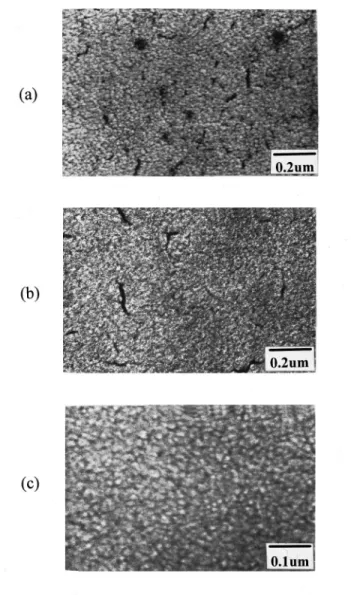
Figure 1 shows the surface morphology of the as-deposited Cr–O and Cr–N–O films. Cracks can be seen on the surface of sample A@Fig. 1~a!# and sample B @Fig. 1~b!#,
which were, respectively, not doped and lightly doped with nitrogen. For the nitrogen doped sample C, a smooth surface was observed @Fig. 1~c!#. The surface morphology of the Cr–O film can be improved by nitrogen incorporation.
XPS30 analysis indicated that oxygen was present throughout the Cr–O and Cr–N–O films, but not in the un-derlying Cu layer. ~The XPS instrument used in this study was the model: ESCA PHI 1600 of Perkin Elmer. All the XPS binding energies were calibrated using the binding en-ergy of surface absorbed carbon C 1s photoelectrons, which is 284.5 eV.30! The nitrogen of both samples B and C was determined to be in the Cr nitride (Cr2N) phase based on the binding energy of N 1s photoelectrons measured to be 397.4 eV. On the top surface, Cr 2p3/2 and O 1s photoelectrons were utilized to determine that oxygen was present only in the Cr2O3phase, whose binding energies were determined to be 576.8 and 531.4 eV, respectively, presumably resulting from the air exposure. However, inside the Cr–O and Cr– N–O layers for all samples, only unreacted oxygen was present based on Cr 2p3/2 and O 1s photoelectron binding energies of 574.4 and 531.0 eV, respectively.
The oxygen and nitrogen contents, as determined by AES analysis, along with the resistivity, as determined from the sheet resistance and thickness measurements, are tabulated in Table I for the as-deposited films. It can be seen that nitrogen incorporation resulted in reduced resistivity.
B. Thermal annealing in N2ambient
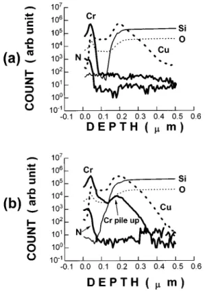
Figures 2 and 3 show the SIMS depth profiles for the as-deposited as well as the 500 °C annealed samples A and TABLE I. Deposition conditions and specific parameters of as-deposited
Cr–O and Cr–N–O films.
Sample identification A ~Cr–O! B ~Cr–N–O! C ~Cr–N–O!
Partial pressure of N2in sputtering gas~mTorr!
0 0.195 1.56 Deposition power~W! 100 150 150 Deposition rate~Å/s! 0.3 0.4 0.4 Resistivity~mV cm! 8.7 7.5 5.3 Nitrogen atomic concentration~%! 0a 0a 30 Oxygen atomic concentration~%! 35 35 25 a
Below detection limit.
FIG. 1. SEM micrographs showing surface morphology of as-deposited~a! sample A,~b! sample B, and ~c! sample C.
FIG. 2. SIMS depth profiles for sample A~a! as-deposited and ~b! 500 °C N2 annealed.
C, respectively. ~The penetration of Cu into SiO2 is com-monly observed because there is no barrier layer separating the sputter deposition of Cu on the SiO2 substrate.! For sample A, the Cu profile remained nearly unchanged after annealing@Fig. 2~b!# as compared with the as-deposited pro-file @Fig. 2~a!#, while the N and Cr profiles revealed signifi-cant change. The N signal in the passivation layer of the annealed sample increased two orders of magnitude over the as-deposited film. The Cr profile reveals a Cr pileup at the Cu/SiO2 interface. For sample C ~Fig. 3!, N2 annealing did not change the Cu or N profile, while a similar pileup of Cr was found at the Cu/SiO2 interface.
The 500 and 700 °C annealed samples of B as well as C were analyzed by XPS.30 Similar results were obtained for the B and C samples. Based on the measured binding ener-gies of Cr 2p3/2, N 1s, and O 1s photoelectrons, we deter-mined that the Cr in the Cr–N–O layer was a mixture of elemental and nitride (Cr2N) states, and only unreacted oxy-gen was present throughout the entire passivation layer. Be-cause no copper signal was found in the passivation layers, thermal annealing in N2only nitrided the passivation layer of sample B, and presumably only sintered that of sample C; these nitrided and/or sintered passivation layers protected the underlying Cu layer from being oxidized by the oxygen in-corporated in the passivation layer and the residual oxygen in the annealing ambient.
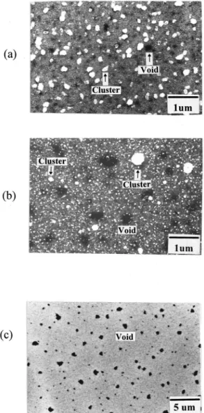
Figure 4 shows the surface morphology of sample B fol-lowing annealing in a N2ambient. Figures 4~a! and 4~b! are following a 500 °C anneal with Fig. 4~b! a 203 magnifica-tion of Fig. 4~a!. Figure 4~c! shows the surface morphology
following a 700 °C N2 anneal. Similar cluster and void for-mation was observed on the annealed samples of A and B. For sample B annealed at 700 °C, clusters were no longer visible, as shown in Fig. 4~c!. Figure 5 shows the surface morphology of sample C annealed in a N2ambient at various temperatures; voids are clearly observed on the surface, but clusters did not appear.
Voids were observed for all samples thermally annealed in a N2ambient at elevated temperatures. Voids~Figs. 4 and 5! could arise from the agglomeration of the film due to the mismatch of the thermal expansion coefficient between Cr– N–O and Cu as well as the volume difference of Cr and Cr2N. Another possibility is the Kirkendall effect
31
resulting from the higher diffusivity of Cr as compared with Cu.3,27 This could result in the movement of more Cr than Cu, lead-ing to a coalescence of vacancies into voids. The movement of Cr could explain the Cr pileup at the Cu/SiO2 interface observed in the SIMS profiles.
FIG. 3. SIMS depth profiles for sample C~a! as-deposited and ~b! 500 °C N2 annealed.
FIG. 4. SEM micrographs showing surface morphology for sample B an-nealed at~a! and ~b! 500 °C, and ~c! 700 °C. The micrographs ~b! and ~c! have a 20 times magnification of micrograph~a!.
For samples A and B, which were nitrogen deficient in the as-deposited passivation layers, the nitrogen for doping and/or nitridation came from the flowing N2ambient during the thermal N2annealing. It was easier to form Cr nitride on the film surface than inside the film because there were many more nucleation sites on the surface. Thus, the clusters that were observed in low temperature annealed samples A and B @Figs. 4~a! and 4~b!# were presumed to be Cr2N. As the annealing temperature was raised high enough, the Cr2N clusters nucleated into a continuous layer, thus no cluster was observed @Fig. 4~c!#. For sample Cs, whose Cr–N–O passivation layers contained plenty of nitrogen, thermal N2 annealing resulted in little change in the N profile ~Fig. 3! and no clusters were observed ~Fig. 5!; this is because the nucleation of Cr nitride occurred mostly inside the nitrogen sufficient Cr–N–O layer.
The electrical resistivity of all samples annealed in a N2 ambient reached a low value of approximately 3 mV cm, which was determined simply by taking the product of mea-sured sheet resistance and the layer thickness meamea-sured from the outermost surface to the Cu/SiO2interface. The
resistiv-ity is very likely overestimated using this approach. Since 1% ~atomic concentration! an increase of Cr in Cu would result in about a 4 mV cm resistivity increase,3,4,32 we esti-mate that less than 1% of the Cr diffused into the Cu after N2 annealing at 700 °C.
No Cu oxide was detected for any of the samples~A, B, and C! annealed in a N2 ambient at temperatures up to 700 °C by the analytical instruments used in this study. In-stead, the thermal N2annealing results in nitridation and sin-tering.
C. Thermal annealing in O2ambient
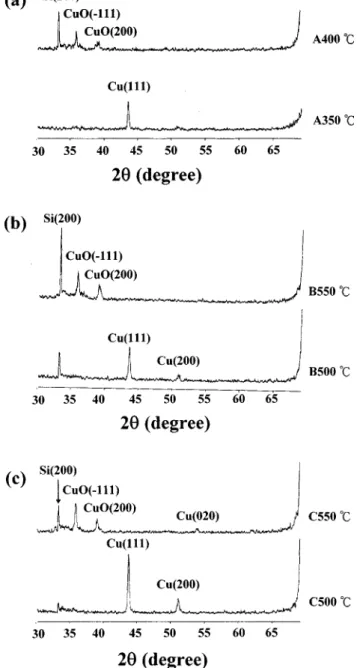
Figure 6 shows the XRD spectra for the samples ther-mally annealed in an O2 ambient at temperatures below as FIG. 5. SEM micrographs showing surface morphology for sample C
an-nealed at~a! 400 °C, ~b! 500 °C, and ~c! 700 °C in N2ambient.
FIG. 6. XRD spectra for~a! sample A, ~b! sample B, and ~c! sample C thermally annealed in O2ambient at temperatures below as well as above their respective temperatures of Cu oxide appearance.
well as above the temperature of copper oxide phase appear-ance. For sample A, which is a Cr–O layer without nitrogen doping, the effective range of passivation against Cu oxida-tion was found to be below 400 °C@Fig. 6~a!#. For sample B, which is a Cr–N–O layer with very low level nitrogen dop-ing, the effective range of passivation against Cu oxidation was raised to 500 °C @Fig. 6~b!#. For sample C, which is a Cr–N–O layer with a high level of nitrogen doping, the ef-fective range of passivation against Cu oxidation was also found to be up to 500 °C @Fig. 6~c!#.
Figure 7 shows the surface morphology for the samples annealed in an O2 ambient. Low temperature ~250 °C! an-nealing of sample A resulted in clusters and voids@Fig. 7~a!#. For sample B, clusters were not observed after annealing at temperatures below 450 °C, but appeared when the annealing temperature was raised to 450 °C@Fig. 7~b!#. For sample C, no clusters were found after annealing at temperatures up to 500 °C@Fig. 7~c!#.
XPS analysis with sequential ion milling provided an
in-depth profile30 of the 500 °C annealed sample B. On the outermost surface, the Cu 2p3/2, Cr 2p3/2, and O 1s photo-electrons, with binding energies at 934.0, 578.0, and 531.6 eV, respectively, were detected. As the surface region was sputter removed, the Cu 2p3/2 photoelectrons disappeared, while the binding energies of Cr 2p3/2 and O 1s photoelec-trons shifted to 576.8 and 531.4 eV, respectively, which be-long to the Cr2O3state. The results indicated that a thin oxide (CuCr2O4) layer was present on the outermost surface fol-lowed by a much thicker underlying layer of Cr2O3. No N 1s photoelectron signal was detected. Moreover, the Cu 2p3/2 photoelectrons underneath the Cr2O3 layer remained in the elemental state, indicating no oxidation of the underlying Cu layer.
The results of XPS analysis with sequential ion milling for the 500 °C annealed sample C showed that the nitrogen was present in both the elemental and Cr2N phases based on the N 1s photoelectron binding energies of 398.2 and 397.4 eV, respectively, as shown in Fig. 8. The surface was cov-ered with a Cr2O3outerlayer. A Cu signal was detected only underneath the Cr2O3layer, and the Cu 2p3/2 photoelectrons underneath the Cr2O3layer remained in the elemental state, indicating no oxidation of the Cu layer.
The surface defects provided easy diffusion paths1,5,7–12 for oxygen and copper through the Cr–O layer, such as was the case for sample A shown in Fig. 1~a!. With nitrogen incorporation into the passivation layer, the diffusion paths along the grain boundaries and the defects in samples B and C were decorated due to the nitrogen stuffing.12,33Moreover, thermal annealing in an O2 ambient resulted in formation of Cr oxide3,4,27,28 as well as healing of the defects and thus obstructing the diffusion of copper and oxygen. For sample B, however, because of the deficiency of nitrogen, Cu dif-fused to the surface through defects and reacted with Cr and oxygen to form CuCr2O4 on the outermost surface at the beginning of thermal annealing. As the diffusion paths of Cu were blocked by the formation of CuCr2O4 or impeded by the defect healing, oxidation of Cu ceased but oxidation of Cr continued.3,4,27,28For sample C, which has a much higher FIG. 7. SEM micrographs showing surface morphology for the samples
annealed in O2ambient~a! sample A annealed at 250 °C, ~b! sample B annealed at 450 °C, and~c! sample C annealed at 500 °C.
FIG. 8. Chemical states and binding energies of the N 1s photoelectrons for sample C annealed in O2ambient at 500 °C.
level of nitrogen doping than sample B and has a very smooth surface morphology @Fig. 1~c!#, annealing at 500 °C in O2 ambient resulted in only Cr2O3 formation on the sur-face because there was no easy path for outdiffusion of Cu. Therefore, no copper oxide phase should be detected before the passivation layer was completely consumed, and the re-sults of XPS analysis seem to support this presumption.
IV. SUMMARY AND CONCLUSION
Copper films passivated by a 200 Å sputter deposited Cr–O or reactively sputter deposited Cr–N–O layer were studied with respect to their passivation capability against thermal oxidation of Cu in flowing nitrogen and flowing oxy-gen ambients. The thermal N2 annealing is essentially a ni-tridation and sintering process. The electrical resistivity of samples thermally annealed in N2 reached a low value of about 3 mV cm, and we estimated that less than 1% ~atomic concentration! of Cr resided in Cu after N2 annealing at 700 °C. Both Cr–O and Cr–N–O passivation layers were able to prohibit oxidation of Cu at temperatures up to 700 °C. In an O2ambient, the passivation capability of Cr– N–O layer was found to be 500 °C, which is 150 °C higher than that of the Cr–O layer. Without nitrogen doping, there were cracks on the sputter deposited Cr–O layer, which pre-sumably provided fast diffusion paths for oxygen and cop-per. With proper nitrogen doping, the reactive sputtered Cr– N–O layer has a very smooth surface morphology. We assume that the nitrogen doping resulted in the formation of Cr nitride in the Cr–N–O layers as well as decorated the diffusion paths, thus efficiently improving the passivation ca-pability. Thermal annealing of the Cr–N–O/Cu/SiO2/Si structure in an O2ambient indicated that the nitrogen doped Cr–N–O layer is effective in serving as a passivation layer against Cu oxidation up to 500 °C.
ACKNOWLEDGMENTS
The authors wish to thank the Semiconductor Research Center of National Chiao-Tung University for providing ex-cellent processing environment. This work was supported by the National Science Council, Republic of China under Con-tract No. NSC-86-2215-E-009-040.
1
See, for example, Mater. Res. Soc. Bull. 18~1993!; 19 ~1994!, devoted to the topic of Copper Metallization for Microelectronics.
2K. P. Rodbell, E. G. Colgan, and C.-K. Hu, Mater. Res. Soc. Symp. Proc. 337, 59~1994!.
3CRC Handbook of Chemistry and Physics, 73rd ed., edited by D. R. Lide
~CRC, Boca Raton, FL, 1992!, Sec. 12.
4Binary Alloy Phase Diagrams, 2nd ed., edited by T. B. Massalski~ASM International, Material Park, OH, 1990!, pp. 1266, 1293, 1304, and 1446. 5
S. Shingubara, K. Fujiki, A. Sano, H. Sakaue, and Y. Horiike, Mater. Res. Soc. Symp. Proc. 338, 441~1994!.
6
Y. Igarashi, T. Yamanobe, and T. Ito, Thin Solid Films 262, 124~1995!. 7J. D. McBrayer, R. M. Swanson, and T. W. Sigmon, J. Electrochem. Soc.
133, 1242~1986!.
8Y. Shacham-Diamand, A. Dedhia, D. Hoffstetter, and W. G. Oldham, J. Electrochem. Soc. 140, 2427~1993!.
9D. Gupta, Mater. Res. Soc. Symp. Proc. 337, 209~1994!. 10
G. Raghavan, C. Chiang, P. B. Anders, S. M. Tzeng, R. Villasol, G. Bai, M. Bohr, and D. B. Fraser, Thin Solid Films 262, 168~1995!. 11
VLSI Technology, 2nd ed., edited by S. M. Sze~McGraw-Hill, Singapore,
1988!, p. 309. 12
S. Q. Wang, S. Suthar, C. Hoeflich, and B. J. Burrow, J. Appl. Phys. 73, 2301~1993!.
13
J. Li, J. W. Mayer, and E. G. Colgan, J. Appl. Phys. 70, 2820~1991!. 14M. O’Reilly, X. Jiang, J. T. Beechinor, S. Lynch, C. N. Dheasuna, J. C.
Patterson, and G. M. Crean, Appl. Surf. Sci. 91, 152~1995!.
15H. K. Liou, J. S. Huang, and K. N. Tu, J. Appl. Phys. 77, 5443~1995!. 16A. J. Griffin, Jr., S. E. Herna´ndez, and F. K. Brotzen, J. Electrochem. Soc.
141, 807~1994!.
17W. A. Lanford, P. J. Ding, W. Wang, S. Hymes, and S. P. Murarka, Thin Solid Films 262, 234~1995!.
18P. J. Ding, W. Wang, W. A. Lanford, S. Hymes, and S. P. Murarka, Appl. Phys. Lett. 65, 1778~1994!.
19J. Li, J. W. Mayer, Y. Shacham-Diamand, and E. G. Colgan, Appl. Phys. Lett. 60, 2983~1992!.
20
H. Itow, Y. Nakasaki, G. Minamihaba, K. Suguro, and H. Okano, Appl. Phys. Lett. 63, 934~1993!.
21
D. S. Gardner, J. Onuki, K. Kudoo, Y. Misawa, and Q. T. Vu, Thin Solid Films 262, 104~1995!.
22Y. Igarashi, T. Yamanobe, T. Yamaji, S. Nishikawa, and T. Ito, Jpn. J. Appl. Phys., Part 1 33, 462~1994!.
23S. Hymes, S. P. Murarka, C. Shepard, and W. A. Lanford, J. Appl. Phys. 71, 4623~1992!.
24
P. J. Ding, W. A. Lanford, S. Hymes, and S. P. Murarka, J. Appl. Phys. 74, 1331~1993!.
25F. Cosset, G. Contoux, A. Celerier, and J. Machet, Surf. Coat. Technol. 79, 25~1996!.
26C. Friedrich, G. Berg, E. Broszeit, and K.-H. Kloos, Surf. Coat. Technol. 74–75, 279~1995!.
27E. A. Brandes, Smithells Metals Handbook, 6th ed.~Robert Hartnoll, Bodmin, Cornwall, England, 1983!, pp. 8-21–8-25.
28
T. Kacsich and K.-P. Lieb, Thin Solid Films 235, 4~1994!. 29W. Kern and D. A. Puotinen, RCA Rev. 31, 187~1970!.
30Handbook of X-ray Photoelectron Spectroscopy, edited by G. E. Muilen-berg ~Perkin-Elmer Physical Electronics Division, Eden Prairie, MN, 1979!.
31
R. E. Reed-Hill, Physical Metallurgy Principles, 2nd ed.~Van Nostrand, New York, 1972!, pp. 386–390.
32C. Cabral, Jr., J. M. E. Harper, K. Holloway, D. A. Smith, and R. G. Schad, J. Vac. Sci. Technol. A 10, 1706~1992!.
33J.-C. Chiou, K.-C. Juang, and M.-C. Chen, J. Electrochem. Soc. 142, 2326~1995!.