國 立 交 通 大 學
電子工程學系電子研究所
博 士 論 文
砷化銦量子點之材料特性及雷射行為
InAs Quantum Dot:Material Characterization and Lasing
Behavior
研 究 生 :王 興 燁
指導教授 :李 建 平
砷化銦量子點之材料特性及雷射行為
學生:王興燁 指導教授:李建平
國 立 交 通 大 學
電子工程學系電子研究所
摘 要
本論文的目的在研究自組式量子點的成長,結構特性以及半導體雷射二極體的應 用。我們針對三個主要課題進行研究 : (1)利用離子通道量测技術來探測砷化銦量子點 的應變分佈(2)研究量子點雷射波長切換的行為(3)量子點在質變形緩衝層基板上的生 長行為。 在離子通道技術中,若使用較輕的離子(氫)當作離子源來研究自組式砷化銦量子點 的應變,會受限它超薄的厚度而無法獲得清楚的資訊。在我們的研究,我們使用了較重 的離子(碳)為離子源,所以應變的資訊可以被獲得。我們的結果顯示砷化銦量子點和砷 化鎵基板的晶格在垂直成長方向是相同的。砷化銦在成長方向的晶格則大於砷化鎵基板 子此一方向的晶格。在我們的研究中也分析退火處理後的量子點應變變化。結果顯示應 變鬆弛先發生在成長方向接發生在垂直成長方向。 從光譜的顯示,砷化銦量子點雷射會存在基態和激發態兩個雷射波長的光,如何使 單一量子點雷射在這兩個雷射能譜之間切換,對進一步量子點雷射的應用有莫大的幫 助。因此我們也研究基態和激發態兩個雷射波長的光相互切換的行為,在此研究分成兩 個部份,其一研究單一共振腔在不同雷射光能譜之間切換行為,另外我們也利用雙共振 腔來達成不同雷射光能譜之間切換行為。在單一共振腔量子點雷射,我們發現改變不同 的電流,共振腔長度以及操作溫度都可以讓雷射在不同雷射光能譜之間進行切換。若使 用雙共振腔雷射則可以使量子點雷射快速在這兩雷射波長之間切換。 本研究最後一部分是探討砷化銦量子點生長在質變形緩衝層基板上的生長行為,當 砷化銦量子點長在質變形緩衝層基板上,有一最大的優點是可以讓砷化銦量子點發出更 長波長的光,對進一步將砷化銦量子點雷射應用在光通訊上非常有用。由於質變形緩衝 層基板內的殘存應變會影響量子點的生長行為,而此一研究主題仍未被探討,因此我們就針對此一主題做了有系統的研究。結果發現,量子點會選擇性的生長在某些區域。這 種選擇性的生長來自於應變不均於分佈在質變形緩衝層基板。
InAs Quantum Dot:Material Characterization and Lasing Behavior
Student: Hsing-Yeh Wang Advisor: Dr. Chien-Ping, Lee
Department of Electronic Engineering and Institute of Electronic Engineering National Chiao Tung University
Abstract
The growth and the characteristic of self-assembled InAs quantum dots (QDs) and its laser applications are investigated in this dissertation. Three topics are covered: (1) understanding the structure of quantum dots (i.e., strain) through the strain measurement using ion channeling technique; (2) investigating the wavelength switching of quantum dots lasers; (3) understanding the behavior of InAs QD growth on the metamorphic structure.
Ion channeling technique using MeV C++ ions was used to study strain in self-assembled InAs QDs buried in GaAs matrix. Because of the use of heaving ions, we were able to observe an angular shift in the angular scan of the In signal relative to that of the Ga/As signal. This provided a direct evidence that the InAs lattice is larger than that of GaAs in the growth direction. Combing the channeling results in [100] and [110] directions and the photoluminescence emission spectrum, we conclude that the InAs QDs are under tensile strain in the growth direction and have the same lattice constant as that of GaAs in the lateral direction. Thermal annealing causes the strain to relax, first in the growth direction and then in the lateral direction as the annealing temperature increases. The photoluminescence spectra of the QDs before and after annealing indicate, however, that composition intermixing also takes place during annealing and is the dominant factor in determining the band gap energy of the QDs.
For InAs QD lasers, distinct peaks in the optical spectra reveal that both the ground state and the excited state transitions can participate in lasing action. The wavelength switching behavior (from the ground state to the excited state transition) of InAs QD lasers cavity was investigated in this study. For QD lasers with single cavity, the results show that wavelength switching could be achieved by driving the device at different currents, and changing the cavity length and the operation temperature. At low current, the ground state lasing threshold is reached. With increasing driving currents, the excited state lasing threshold is reached, which indicates two-state lasing transitions occurred. Then lasing transition switches
completely changed to the excited state transition. At room temperature, we observed a switching of the lasing wavelength from the ground state to the excited state transition at the critical cavity length (1100 μm). The excited state lasing threshold do not occur when the cavity length was longer than 1500 μm. The ground state (excited state) lasing threshold increases (decreases) with increasing operation temperature.
We also demonstrated two-state switching, between the ground state ~1.3 μm and the excited state ~1.2 μm, of an InAs QD laser using a two-section QD laser. Mode switching was achieved by adjusting the gain of each section by the current injected into that section. With a constant total current, we were able to switch between 1.2 μm emission and 1.3 μm emission simply by adjusting the current ratio applied to the two sections.
Finally, the growth behavior of InAs QDs on the metamorphic buffer layer had been studies in this study. The AFM and TEM images show the selective growth of QDs on the InGaAs layer. The growth behavior was controlled by the amplitude of the modulation of the growth surface. Two factors can affect the amplitude of the surface modulation of the growth surface. One factor is the amount of decreased indium content in the top layer above the metamorphic buffer layer. Another is the growth temperature of the metamorphic buffer.
In total, this study has hard offered abundant data in the growth behavior and the strain information of self assembled InAs quantum dots and its laser applications.
誌謝 完成這份論文,最要感謝的是我的指導老師李建平教授,他提供了一個優質的研究環 境,更潛移默化的培養我獨立研究的能力。在這段期間,他不僅給我學問上的指導,我 也從他身上學會許多待人處世的道理,因此這段期間可以說是我個人獲益最豐富的一段 期間。也要感謝林聖迪學長,他不僅在實驗上幫助我,更不吝惜的提供建議,使我的研 究成果更加優質。當然也要感謝這幾年一起工作學長學弟們,像李秉奇,林志昌、羅明 城、凌鴻旭、大君等,要是沒有你們幫忙與參與,我的研究必定是困難重重。還有牛寰、 陳建旭、楊仁盛及鄭旭傑,因為曾與你們一起研究,培養了深厚的情誼,過程中更使我 領悟到一些團隊工作所需能力,相信對未來必定有所幫助。 最後要感謝我的家人及太太劉靜芳,若沒有你們默默支持與鼓勵,真不知是否能完成這 份論文。今後若我真有什麼成就,你們才是這一切的推手。
CONTENTS
Abstract (Chinese) i
Abstract (English) iii
Acknowledgement v
Contents vi
Table Captions ix
Figure Captions x
Chapter 1 Introduction
1.1 Strain Measurement of Quantum Dots by Ion Channeling Technique 11.2 Wavelength Switching in Quantum Dot Lasers 3
1.3 QDs growth on the metamorphic structure 3
1.4 Organization of Dissertation 5
Chapter 2 Experimental techniques
2.1 Molecular Beam Epitaxy system 62.1.1 Introduction of System 6
2.1.2 Reflection High-Energy Electron Diffraction (RHEED) 9
2.1.3 Pre-growth Procedure and Growth Conditions 11
2.2 MeV ion channeling as instrument for materials analysis
12
2.2.1 Rutherford Backscattering Spectrum 12
2.2.2 Angular Scan Curve 15
2.2.3 Tetragonal Deformation of Thin-film in MeV Measurement 15
2.2.4 Ion Channeling Set-up 17
2.3 Optical Measurement 18
Chapter 3 Strain Study of Quantum Dots by Ion Channeling
Technique
3.1 Introduction 213.2 The Buried InAs Quantum dot was Probe by Heavy Incoming Ions 21
3.3 Sample structure and Measurement Condition 24
3.4 Results of Angular Scan Curves 25
3.5 The Strain State along Growth Direction 32
3.6 The Relationship between Optical properties and Strain State 33
3.7 Conclusion 34
Chapter 4 The wavelength switching Transition in quantum dots
lasers
4.1 Introduction 364.2 Device Growth 36
4.3 Device Process 38
4.4 Characteristic Measurement System 40
4.5 Lasing switching in single cavity QD lasers 41
4.5.1 Using Different Drive Currents 41
4.5.2 Cavity Length and Operation Temperature 43
4.5.3 Conclusion 48
4.6 The Wavelength Switching Transition in Coupled-cavity Lasers 49
4.6.1 Introduction 49
4.6.2 Sample Growth and Device Structure 50
4.6.3 Result and Discussions 51
4.6.4 Conclusion 54
Chapter 5 The Growth Behavior of InAs QDs on InAlAs/GaAs
Metamorphic Buffer Layer
5.1 Introduction 555.2 Strain Relaxation of the Metamorphic Buffers 55
5.3 Sample Growth 56
5.4 The Growth Behavior of the InAs QDs with Different Indium Composition 59 5.5 The Growth behavior of the InAs QDs with Different Growth
Temperatures of the Buffer Layer 69 5.6 Conclusion 72
Chapter 6 Summary
74Reference
76Vita
Publication List
Table Captions
Table 5.1 Final In content and growth temperature in graded buffer layer, In composition in the InAlAs inverse layer and InGaAs layers for all samples.
Figure Captions
FIG. 2.1 A schematic of our Gen II MBE system.
FIG. 2.2 The schematic representation showing the interaction of the Ewald sphere with reciprocal lattice rods in RHEED analysis of a two-dimensional surface net.
FIG. 2.3 Schematic of the energy spectrum of particles scattering from a solid composed of a substrate (M2,Z2) and the epilayer (M3,Z3). The left of this figure show the angular scan curves of the substrate and the epilayer.
FIG. 2.4 The deformation of the epi-layer causes the different off-normal crystal axes between the epi-layer and the substrate.
FIG. 2.5 The measured Si (substrate) and SiGe (strained epi-layer) angular scans of the [111] axis. (after L. J. M. Selen. et al., 2003)
FIG. 2.6 The whole scheme drawings of the channeling experiment
FIG. 2.7 The schematic structure of PL measurement system
FIG. 3.1 Calculated result of close-encounter probability of C++ (dot line) and He+ (solid line) ions impinging on a [100] GaAs surface versus the depth from surface.
FIG. 3.2 The structure of our samples. InAs QDs grown on the GaAs substrate. InAs QDs were embedded 50 nm below the surface.
FIG. 3.3 Schematic diagram of how a buried strained layer is probed by ion beam
FIG. 3.4 Backscattering spectrum shows the In and GaAs signal are separated completely. Tight figure shows the angular scan curve, the curve provide strain information. In signal is the integral over the whole In peak In backscattering spectrum from 1200 to 1300 channel. GaAs signal is integral from 800 nm to 40nm channel.
FIG. 3.5. Angular scan spectra along (a) [100] and (b) [110] axes of the as-grown QD sample. The angular shift was determined by the relative change in angle position of the half maximum of the In and Ga/As curves on either side of the channeling curves. From the sign of (∆θ)right -(∆θ)left, we determine which direction the
curves shift relative to each other. No obvious difference was observed between the curves of In and Ga/As in the [100] direction. In the [110] direction, we observe an angular shift of the In signal relative to the Ga/As signal toward the [100] direction.
FIG. 3.6. Angular scan spectra of the QDs annealed at 650oC. The In and Ga/As signal again match in the [100] direction. In the [110] direction, the angular shift of the In signal becomes larger than that of the as-grown sample.
FIG. 3.7. Angular scan spectra of the QDs annealed at 750oC. In the [100] direction, the In signal is narrower than that of the Ga/As signal. In the [110] direction, the angular scan spectra are similar to those of the sample annealed at 650°C.
FIG. 3.8. Photoluminescence spectra at 25 K of QDs before and after annealing.
FIG. 4.1. The growth sequence of laser is schematically shown. The hetero-structure for QDs were grown by MBE.
FIG. 4.2. The conventional ridge waveguide structure was fabricated with standard procedure.
FIG 4.3. The schematic diagram for the measurement of L-I characteristics
FIG. 4.4 The results L-I curve of QDs laser and the optical spectrum with varied bias currents, respectively. In the QDs laser, cavity width is 20 μm and cavity length is 1.4 mm.
(b)1.2mm(c)1.3mm(d)1.4mm(e)1.5mm. L-I curves were measured at various operation temperatures.
FIG. 4.6 The inverse of the slope efficiency is the function of cavity length.
FIG. 4.7 Schematic of the two-section laser structure
FIG. 4.8 Lasing mode distribution vs input currents to the two sections of the laser cavity.
FIG. 4.9 Lasing mode switching by adjusting the ratio of the currents injected into the two sections. The three spectra, corresponding to ground state, dual state, and excited lasing, were measured along a constant current line with a total current of 225 mA.
FIG. 5.1 The schematic drawing of the metamorphic structure of the samples and their indium composition profile.
FIG. 5.2 (a)AFM images with 5x5 μm2 scanned area. (b) the AFM images of 2x2 μm2
taken on the positions ‘a’, as indicated in Fig. (a).
Fig. 5.3 (a) AFM images with 5x5 μm2 scanned area. (b)The AFM images of 2x2 μm2
taken on the positions ‘a’, as indicated in (a). (c) surface height profile in (b).
Fig. 5.4 (a) AFM images with 5x5 μm2 VOF. (b)The AFM images of 2x2 μm2 taken on the
positions ‘a’, as indicated in (a).
FIG. 5.5 (a) The TEM images for sample B. The image reveals the selective growth of InAs QDs. The embedded QDs layer still exist QDs. The QD distribution for embedded layer is the same as the surface. (b) the region without QDs under higher magnitude. The embedded QDs layer don’t exist QDs. (c) the region with QDs using higher magnification.
growth. The QDs distribution for embedded layer is same as the surface. (b) TEM image with higher magnification.
Fig. 5.7 The low temperature photoluminescence measurement off sample A, B and C.
FIG. 5.8 (a) AFM images with 5x5 μm2 scanned area. (b) surface height profile.
FIG. 5.9 AFM images of sample with 5x5 μm2 scanned area. Result shows poor crystal
Chapter 1
Introduction
Quantum dots (QDs) have size quantization in three directions. The discrete nature of the energy levels and the associated density of states make QDs attractive for many device applications. For example, semiconductor lasers based on QDs have demonstrated in lower threshold current densities, low temperature sensitivity and higher gain [1]. Over the last decade there has been a large amount of interests in QD researches for further developments of opoto-electronic devices. One of interests is to develop semiconductor lasers in the wavelength range of 1.3 μm to 1.55 μm for fiber optical communications. Self-assemble InAs QD laser on GaAs substrate is one of important approaches for this purpose. In this dissertation, we present our InAs QD studies related to the development of powerful semiconductor lasers from three different aspects: (1) understanding the structure of quantum dots (i.e. strain) through the strain measurement using ion channeling technique; (2) investigating the wavelength switching of quantum dots lasers; (3) understanding the behavior of InAs QD growth on the metamorphic structure.
1.1 Strain Measurement of Quantum Dots by Ion Channeling Technique
Because of large lattice mismatched between InAs and GaAs substrate (i.e. 7%), the growth of thick epilayers is usually impossible. However, the formation of dislocation-free coherent islands of InAs on the GaAs has been observed [2-12]. This island formation has been attributed to the transition from a two-dimensional growth mode to a three-dimensional one. It is driven by the strain originated from the lattice mismatch between InAs and GaAs. Thus, the strain distribution in and around the dots not only governs the dot formation and
geometry, but it also has a strong influence on the electronic structure of the dots [13-15]. The information of strain distribution becomes important. Up to date, there are very limited experimental data available about the strain in and around the dots. Conventional high-resolution x-ray diffraction of InAs quantum dot layers has difficulty in obtaining the detail information on the strain distribution due to problems like insufficient light intensity, the lack of smooth interface, and the low degree of periodicity [16,17]. Grazing-incidence x-ray diffraction is able to clearly measure the structure characteristics of uncapped dots, but it is not easy to determine strain distribution of buried dots [18]. Techniques with atomic resolution have been used including transmission electron microscopy [19,20], atomic force microscopy [21,22] and scanning tunneling microscopy [23]. However, these techniques are either destructive or they cannot be used for samples with cap layers. As a result, the information of strain distribution of dots is still absent, particularly for buried dots.
Because the limitation of the above mentioned techniques in probing QD strain, the new approaches are necessary. Ion channeling technique is a powerful tool to probe the strain of quantum wells. This technique uses an ion beam operated in the energy range of MeV to bombard the sample. Under conditions of MeV ions and wavelength range of 10-12 cm, the crystal lattice is not regarded as a diffraction grating but rather as rows or sheets of atoms. The technique is highly sensitive to atomic displacements. For self-assembled quantum dots, the strain distribution is associated to the lattice displacement. By probing atomic displacement, the strain information can be obtained. Recently, one study has attempted to study the strain of QDs using this technique. However, the result was not very clear because the limited height of ultra thin QDs. In this dissertation, we explore the strain of QDs using the MeV ion channeling technique. But we replace the normally used protons by the heavy ions C++ as the ion source, which provides much better depth resolution. The strain in the QD layer has been obtained.
1.2 Wavelength Switching in Quantum Dot Lasers
Solid-state light emitting devices with the capability of electrically controlled wavelength switching may become important for read and write operations, chip-to-chip interconnects, mode-locked laser and wavelength division multiplexing. For InAs QD lasers, distinct peaks in the optical spectra reveal that both the ground state and the excited state transitions can participate in lasing action [24,25]. These distinctly separated levels, which are not encountered in quantum well lasers, are only observed in QD lasers. In chapter 4, dual state lasing (ground state~1.3 μm and excited state~1.2 μm) was observed in conventional single cavity ridge waveguide lasers. In addition, we also have demonstrated of electrically controlled wavelength switching in a couple-cavity QD laser.
1.3 QD growth on metamorphic structures
To this date, only InP/InGaAsP material system has been used for 1.3–1.55 μm telecommunication semiconductor lasers. The characteristics of such lasers are limited by several fundamental problems. One of the problems is the insufficient confinement of carriers in the active region [26,27] leading to a poor temperature stability and a high value of threshold current density. InAs/GaAs QDs laser at 1.3 μm with high temperature stability and low threshold current densities have been demonstrated. It is desirable to extent the wavelength of InAs/GaAs QDs lasers to 1.55 μm. Recently, reported papers have demonstrated InAs QDs laser can emit wavelengths at both 1.55 μm(ground state) [28,29] and 1.3 μm(first excited state)[30] using the structure of metamorphic buffers with GaAs substrates. It provides an opportunity for long wavelength, high performance lasers with GaAs substrates.
and the device layers. The buffers serve as the transition region for the lattice parameter to change from that of GaAs to a larger value by growing relaxed, compositionally graded epilayers. In other words, the metamorphic buffers behave as a virtual substrate that can be designed to accommodate the lattice parameter of the topmost structure. Device performance is influenced by the structure, composition and strain relaxation rate of metamorphic buffer. Most studies in InAs QDs grown on the metamorphic buffer focus on the relation of the emission wavelength and the metamorphic buffer layers. The growth behavior of InAs QDs on the metamorphic buffer is still under studies including the size, the shape and the position distribution of QDs. In this work, we present the growth behavior of InAs QDs including an interesting and unique finding discovered in this study.
1.4 Organization of Dissertation
In chapter 2, the experimental techniques in my research are presented. In Section 2.1 we introduce our Molecular Beam Expitaxy system and growth condition of sample. Section 2.2 describes the basic principle of the ion channeling technique. Section 2.3 describes the photoluminescence system.
In chapter 3, we study the strain in self-assembled InAs QDs buried in GaAs matrix using MeV C++ ion-channeling technique. Section 3.2 describes why InAs QDs was probed using heavy ions. Section 3.4 shows the angular scan curve. A little strain behavior was observed in this section. Section 3.5 presents how to determine the strain state along the growth direction. Section 3.6 shows the relationship between the strain state of InAs QDs and the optical property.
In chapter 4, we present wavelength switching transition of QD lasers. Section 4.2, section 4.3 and section 4.4 introduce the standard procedure of laser process and measurement system in this study. Section 4.5 presents the wavelength switching characteristic of InAs QD
lasers with single cavity. Various methods can achieve the ground to excited state lasing switching. Section 4.6 presented wavelength switching transition in couple cavity laser.
In chapter 5, we present InA QD growth on metamorphic hetero-structure. Section 5.2 explains that the indium composition profile affect the residual strain in the hetero-structure. Section 5.4 shows the growth behavior of InAs QDs on metamorphic buffer by adjusting the indium composition profile in the buffer layer. The results are presented from images of the atomic force microscopy and transmission electron microscopy. Section 5.3 shows the growth behavior of QDs was affected by growth temperature of the buffer layer.
In chapter 6, we concluded our researches. The further work also was mentioned in this chapter.
Chapter 2
Experimental Techniques
In this chapter, the experimental techniques in my research were presented. The contents consist of three parts: (1) the molecular beam epitaxy (MBE) system in our laboratory (2) Ion channeling theory, application for material analysis and system setup. (3) Photoluminescence measurement system.
2.1 Molecular Beam Epitaxy System
2.1.1 Introduction of System
Semiconductor Hetero-structures are important materials system for both fundamental physics researches and device applications. The growth of a perfect hetero-structure need own an abrupt interface, uniform and exact compositions of the grown materials with high quality, and a precise doping distribution. In the past decades, many epitaxy techniques have been developed for obtaining high-quality epi-layer and ideal hetero-structure growth. They are liquid-phase epitaxy (LPE), vapor-phase epitaxy (VPE), metal-organic vapor-phase epitaxy (MOVPE), and molecular beam epitaxy (MBE). Among all these techniques, MBE system has been testified to be the most powerful and reliable system due to its ultra-high vacuum (UHV) environment and relatively simple growth mechanism. The high controllability during growth has made it more and more valuable for various applications, especially for advanced researches.
MBE system in our lab is Vecco Gen II molecular beam epitaxy system. All samples in this dissertation were grown in this system. Fig. 2.1 shows the scheme of the system. The MBE system consists of three chambers, the entry/exit (E/E) chamber, the buffer chamber, and the growth chamber. Gate valves are used to connect and isolate the buffer chamber and the other two chambers. Oil-free pumping systems were used in MBE system in order to not containment the growth environment. In the entry/exit chamber, a turbo pump station and a sorption pump are for roughly pumping when we complete the processes of loading and unloading. A cryo-pump was used to maintain the chamber in 10-9 order. The buffer chamber mainly function is to pre-bake samples and isolated the growth chamber from the water in air. Therefore, the chamber generally main the 10-10 vacuum by a high efficiently ion-pump and an assistance TSP. The pumps in the growth chamber include an ion-pump, an cryo-pump and a TSP pump. Because the volume of growth chamber is bigger than other chambers, pumping rate of the pumps in the chamber are higher than in other chambers. The liquid nitrogen was injected into the cryo panel to assist the growth chamber with better vacuum when we grow the samples. Eight effusion cells are installed in growth chamber. Ground III elements were provided from two gallium dells, one aluminum cell and one indium cell. As2 and As4 were
supplied from arsenic cracker cell and arsenic kundsen cell, respectively. silicon and berullium effusion cell offer as n and p type dopant sources in this system. In our MBE system, material systems that could be grown include AlGaAs, InGaAs on GaAs substrates or AlGaAs, InGaAs, and AlInGaAs on InP substrates.
Besides, in the growth chamber, two analysis instruments are installed. One is the residue gas analyzer (RGA), and another is the reflection high-energy electron diffraction (RHEED) monitor. The RGA is used to analyze the residual gas in the chamber and, thereby, to help us to understand the cleanness in the growth chamber. By setting its detection range of the atomic mass unit (AMU) to that one of helium (He, 4), it can also serve as a very sensitive leak detector.
2.1.2 Reflection High-Energy Electron Diffraction (RHEED)
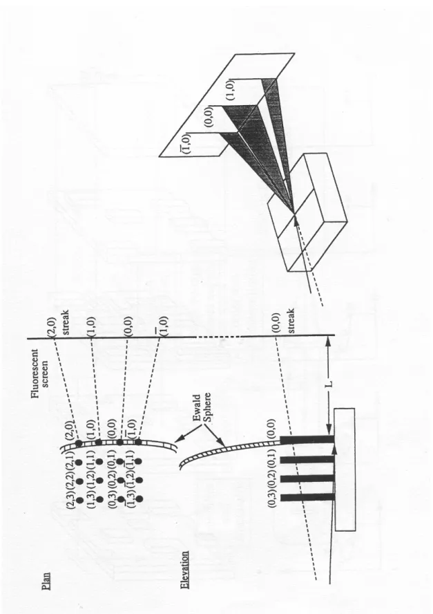
The RHEED allow us to in-situ monitor the surface construction of wafers and epi-layers. In RHEED analysis, a collimated monoenergetic electron beam is directed towards the surface at a grazing angle of about 2 degree and orthogonal to the molecular beam paths, the primary electron energy lies in the range 5~40KeV. Since the energy component perpendicular to the surface is of the order of ~100eV. The penetration depth of the incident electron beam is limited to only the first few atomic layers, as a result, the crystal surface acts as a two dimensional grating and diffracts the incident electron beam. A fluorescent screen placed diametrically opposite the electron gun recorded the diffraction pattern. Because the interaction (diffraction) of the electron beam is essentially with a two-dimensional atomic net for the crystal surface structure, we area concerned with its reciprocal lattice in the reciprocal space which is composed of rods that have a direction normal to the real surface. Fig. 2.2 shows the Ewald sphere and reciprocal lattice rods for a simples square net and the formation of diffraction lines on a plane screen, the surface condition of epitaxial layer can therefore be clearly indicated from the fine details of RHEED patterns.
FIG. 2.2. The schematic representation showing the interaction of the Ewald sphere with reciprocal lattice rods in RHEED analysis of a two-dimensional surface net.
By using RHEED, the construction of a few monolayers on the surface can be analyzed with the diffraction patterns. It makes desorption of native oxide on the surface easy and exact. It can determine whether lattice mismatched hetero-epitaxy retained the layer by layer growth. In general, the 2x4 or 2x8 patterns means the smooth surface during 2D layer growth and native oxide is removed. It is also useful for the growth of quantum dots (QDs), because the 2-D to 3-D transition in QDs formation on the surface could be observed easily from the RHEED pattern transition. Somehow, if the growth mode transformed from the two-dimensional layer by layer growth to the three dimensional island growths, which is the case for the self-assembled quantum dots, the RHEED patterns would change from streaky into spotty patterns. For hetero-structure growth, RHEED is useful tools.
2.1.3 Pre-growth Procedure and Growth Conditions
To maintain the cleanness of the growth chamber and to ensure the quality of grown samples, a standard treatment procedure for wafers before growth is important and necessary. The epi-ready GaAs wafers are mounted on Mo substrate holders with indium or indium-free springs and then put into E/E chamber for bake-out at 200oC, which can remove the water molecules absorbed during the loading procedure. After about two hours bake-out and four hours pumping down, the pressure of the E/E chamber can be lower than 10-8 torr. After that, we transfer the wafers into the buffer chamber, in which the pressure is about 1-5x10⁻¹⁰ torr typically. In this chamber, each wafer is heated to 400oC for over one hour and the chamber pressure is lower than 3x10⁻⁹ torr, in order to remove residual water and organic species. Finally, the wafer could be transferred into the growth chamber. Just before growth, the thin native oxide formed on the wafer surface is decomposed and desorpted by heating under enough arsenic flux. The desorption temperature are about 610oC for GaAs. It should be noted that, before the cells warmed up for sample growth, the growth chamber is cooled down with
the continuously flowed liquid nitrogen and then, typically, the pressure of the chamber lowers from about 3x10⁻⁹ torr to less than 2x10⁻¹⁰ torr.
The growth rate is typically around one µm/hr. The III-V BEP ratio (group V versus group III) and growth temperature must be kept within suitable range for different grown materials for high-quality epi-layers. In general, the growth temperature for AlAs, GaAs and AlxGa1-xAs materials on GaAs substrates are near 575oC for the all the samples studied in this dissertation. The III-V BEP ratio keeps around 10 and 20 for As2 and As4, respectively,
for the growth on GaAs substrate. However, 3-D quantum dots were grown under various growth conditions for the specific propose. They were described in respective chapters for clarity. For InAlAs metamorphic buffer layer, the growth temperature is near 400 oC in order to obtain better strain relaxation layer. The growth conditions depended on the structure recipes. The III-V BEP ratio was more than 20 for As2 in growing metamorphic structure.
2.2 MeV Ion Channeling as Instrument for Materials analysis
2.2.1 Rutherford Backscattering Spectrum
The arrangement of atoms determines the properties of materials. Ion-channeling analysis is a powerful technique to probe the arrangement of atoms in the solid crystal. Rutherford backscattering spectrum (RBS) can resolve the arrangement of lattices and provide angular scan curves, which reveal the deformation information of the epi-layer. In this subsection, we first describe RBS in detail.
In ion channeling technique, the sample is bombarded by using an ion beam operated in the MeV energy range. When a sample is bombarded with MeV ions, the energy of incoming ions transfers to atoms of the sample. The energy transfer depends on how close incoming ions approaches to the atomic nucleus. When the distance between the incoming ion and the atom is at the order of 1 A o, small amount of the energy transfer from incoming ions to the
valence electrons. The energy of incoming ions start losing gradually when the ions penetrate deeper into samples. At smaller distance than 1A°, incoming ions interact with inner electrons and have larger energy transfers. When the distance between the ion and the atom reaches minimum, i.e.the nuclear size, large energy transfers occur and result in the large angle scattering of the incident ion. The process with the large angle scattering of the incoming ion is called the close impact.
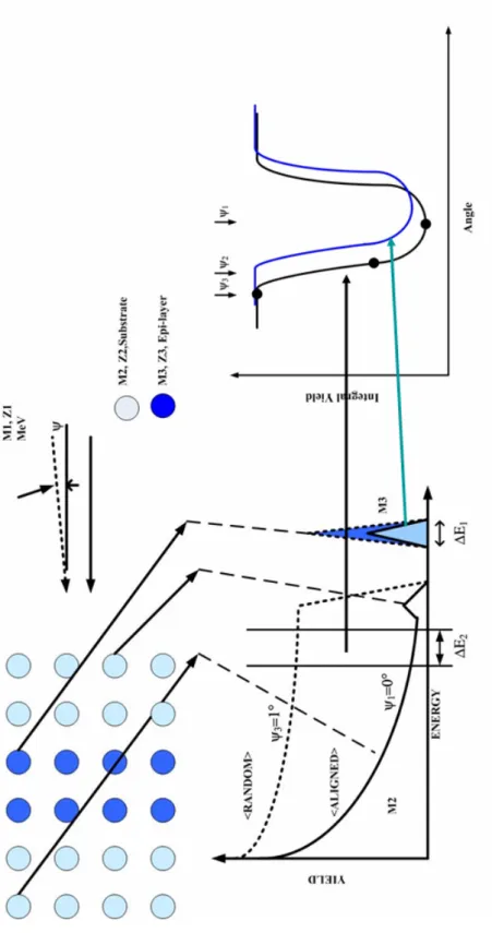
The energy of the incoming ion after large angle scattering event can be revealed by RBS. This energy is determined by the mass and the depth of atoms when the scattering event takes place. An example shown in Fig. 2.3 describes the RBS of an epi-layer structure. A MeV ion beam bombards a sample consisted of a buried epi-layer and a substrate. The atomic mass of the epi-layer is higher than that of the substrate. The bottom portion of Fig. 2.3 shows the RBS of backscattered ions detected by an energy-scan detector. The x-axis represents the energy of backscattered ions. The y-axis represents the scattering yield, which is the number of the backscattered ions. The energy of backscattered ions from the epi-layer with larger atomic mass is higher with finite energy width (i.e., the shadow area in the figure). The broad and continuous spectrum at lower energy represents the energy of backscattered ions from the substrate. The energy distribution of backscattered ions from the epi-layer is separable from the energy of backscattered ions from the substrate when atomic mass is high. Therefore, RBS is suitable for the analysis of heavy atoms in a light substrate.
FIG. 2.3. Schematic of the energy spectrum of particles scattering from a solid composed of a substrate (M2,Z2) and the epilayer (M3,Z3). The left of this figure show the angular scan curves of the substrate and the epilayer.
In Fig. 2.3, the ion beam enters at an incident angle (ψ) respect to the crystal axis within 1°. Less than 2% of incoming ions are backscattered when the incident ion beam aligns with the crystal axis. Thus, the scattering yield in RBS is low as the spectrum with mark, “ALIGNEN”, in the figure. The scattering yield increases when the incident angle of the ion beam increases. It reach maximum when the incident angle is 1° respect to the crystal axis (i.e. the dash line with mark <RANDOM> in the RBS of Fig.2.3)
2.2.2 Angular Scan Curve
A so-called angular scan is the integral of the scattering yield within an interest energy interval as a function of the angle between the incident ion beam and the crystal axis. The right portion of Fig. 2.3 shows the relationship between the angular scan curves and RBS. The angular scan curves of the epi-layer and the substrate are obtained from the energy interval ΔE1 and ΔE2, respectively, as shown with RBS plot. The integral yield from ΔE1 and ΔE2 is
minimum when the incident beam aligns with the crystal axis (angle=0°), and it increases with increasing incident angle.
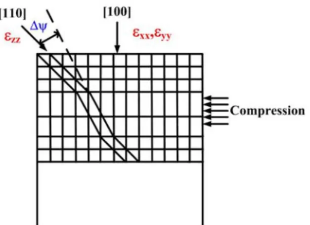
2.2.3Tetragonal Deformation of Epi-layer in MeV Measurement
The tetragonal deformation of the coherent strained epi-layer can be measured from the angular scan curve of the ion-channeling analysis, specifically, by comparing the two minimum yields of the angular scan curves from the strained epi-layer and the substrate. Fig. 2.4 shows deformation of the epi-layer causes the different off-normal crystal axes between the epi-layer and the substrate. It results in the incident angle of the ion beam different relative to the crystal axis of the epi-layer and the substrate. Because the minimum of the angular scan curve is generated when the ion beam is aligned with the crystal axis, so the minimum yield position of the strained epi-layer is different from that of the substrate.
FIG. 2.4. The deformation of the epi-layer causes the different off-normal crystal axes between the epi-layer and the substrate.
Fig. 2.5 shows angular scans for Ge in the strained epi-layer (Si0.8Ge0.2) and Si in the substrate.
In the figure, it indicates that the crystal axis is different between the strained epi-layer and the substrate such that the minima of the strained layer and the substrate are different. The shift between these two curves is to measure the tetragonal distortion in the Si0.8Ge0.2
epi-layer. Thus ion-channeling is an excellent tool for analyzing lattice deformations in crystalline semiconductor structures.
FIG. 2.5. The measured Si (substrate) and SiGe (strained epi-layer) angular scans of the [111] axis. (after L. J. M. Selen. et al., 2003)
2.2.4 Ion Channeling Set-up
An ion channeling experiment requires three basic components: a particle accelerator, vacuum chamber, detector of scattered particles, and an accurate crystal manipulator, a goniometer. In channeling experiment, ion beams are extracted in the energy range of 2-6MeV from the particle accelerator. The ions are transported to the scattering chamber through a beam line. In order to preserve a low angular spread in the ion beam, the pressure in the scattering chamber and the beam line is below 3x10⁻⁸ and 3x10⁻⁵ mbar, respectively.
A high precision goniometer is needed to obtain proper alignment of the target crystal axes or planes with the ion beam. Such a goniometer was designed and constructed at the National Tsing Hua University, with three axes of rotation and three directions of translation. The angular resolution of the goniometer is better than 0.005°. The detector is mounted on a stepper-motor controlled detector disk to obtain a high flexibility in the detector position and
angle, for RBS and transmission channeling experiments. A schematic drawing of the set-up is shown in Fig. 2.6.
2.3 Optical Measurement
Photoluminescence (PL) is a non-destructive characterization technique for optical property of semiconductor. The emission wavelength, peak intensity, and full width at half maximum are the most important for characterizing the quality of epitaxial layers. Fig. 2.7 depicts the schematic of our PL measurement. The exciting light is an Argon laser. The intense spectral emissions around 488 nm and 515 nm are well above the bandgap of investigated materials, such as GaAs, InGaAs, InAs and AlGaAs. The samples are kept in the Helium cryostat which provides for the various temperature measurements. The excitation laser is focused by one lens and the output luminescence is collected by another lens into the input slit of the spectrometer. High-pass filter is put in the input of the spectrometer to block the laser and light with wavelength below 600nm.
The spectrometer is SPEX-1404, 0.85 m double grating monochrometer with ultimate resolution of 0.006 nm. The grating used is 600 /mm with blazing wavelength around 1000 nm. The dispersed light is then imaged into the output slit for detection. Light detection is water-cooled Si photomultiplier or thermal-electrical-cooled InGaAs photodetector, respectively. Si photomultiplier cut off around 1100 nm, the InGaAs detector spans from 800 nm to 1600 nm. The lock-in detection technique is adapted in order to improve ratio of the signal and noise. The excitation light is chopped by a mechanical chopper at frequency of 200~800 Hz. The dispersed and modulated light is then resolved by the lock-in amplifier. The whole measurements are integrated and controlled by the computer.
Chapter 3
Strain Study of Quantum Dots by Ion Channeling Technique
3.1 Introduction
InAs self-assembled quantum dots (QDs) have been extensively used in optoelectronic devices, such as semiconductor lasers [31-33] and detectors [34,35]. The formation of the self-assembled QDs is driven by the strain originated from the lattice mismatch between InAs and GaAs [36]. The physical properties of the dots are strongly dependent on the amount of strain in and around the dots [37]. Strain study of InAs QDs had been deduced by x-ray and transmission electron microscope (TEM). However, the strain of these buried dots is difficult to measure and so far only a very few experimental studies have yielded quantitative information on the strain. MeV ion channeling has long been used in analyzing the atomic ordering in crystal structures and has been successfully applied for the study of strain in quantum wells. In this work, the strain distribution of self-assembled InAs QDs in GaAs was studied using channeling of MeV C++ ions. The strain relaxation of the QDs after thermal annealing was also studied using this technique.
3.2 The Buried InAs Quantum dot was Probe by Heavy Incoming Ions
L. J. M Selen, et al. [38] have studied the strain of buried InAs QDs using He+ MeV ion channeling. However, angular shift in the channeling spectrum caused by strains was not obtained. Because the limited height of QDs, the length of the atomic string along the ion path is not large enough to cause ion steering and a shift in the angular scan. Consequently, it was very difficult to obtain the strain information of the QDs by the angular scan. The experiment
only provided evidence for the presence of strain in and around the QDs. The detailed information of strains is largely unknown.
During ion channeling study, shadow cones are formed by the surface atoms. Only a few layers of atoms close to the surface may contribute to the surface peak. Let us call the thickness of this surface layer the shadow cone length. In the present case, where a thin but strained layer is buried in a crystal matrix, the interface atoms cast a shadow cone on the strained layer underneath from the incoming particles. If we want to investigate the strain by the strain induced steering of channeling ions, the thickness of the thin strained layer has to be larger than the shadow cone length. Then the shift in the angular scan of the backscattered yield provides information of the strain in the strained layer.
Basically, the length of the shadow cone depends on shadow cone radius, Rc, which is given
by E d e Z Z Rc 2 2 1 2 = (3.1)
where Z1 and Z2 are the atomic numbers of the incoming particle and the target atom,
respectively, E is the energy of the incoming particle, and d is the lattice spacing along the channeling direction. Generally, the shadow cone length is reduced if Rc is large [39]. For H+
or He+ ions, Rc is usually pretty small which gives rise to a large shadow cone length. This,
however, posts a problem for the quantum dot samples because the height of the quantum dots, typically only a few nanometers, is smaller than the shadow cone length. Eq. (1) reveals that the shadow cone radius can be increased by reducing the incoming ion’s energy or using heavier ions. Former method, such as medium energy ion scattering (MEIS), has been shown to be useful in analyzing surface structure of thin-films [40,41]. It only probes the surface region that makes it unsuitable for deeply buried thin films, such as QDs. In this study, we chose to use a heavier ion, C++, as incident particles. The shadow cone radius is increased and
the length reduced. We were able to use the shift of the angular scan curves to study the strain of the buried QDs.
To understand the effect of atomic mass of incoming particles on the shadow cone length, we calculated the shadow cone length in GaAs along [100] direction using 4MeV He+ and C++ as incoming particles using the simulation package, FLUX 7, authored by P.J.M. Smulders [42]. The calculated result is shown in Fig. 3.1. The solid and the dotted lines are the close-encounter probability of He+ and C++ ions, respectively. The horizontal axis is the depth from surface. The small Peaks in the carbon close-encounter probability at 28 and 72 angstrom, were caused by the oscillation of particle within the crystal. We can see that the shadow cone length is greatly reduced when C++ is used. At a depth of 15Å, the close encounter probability drops more than 100% because of the use of C++. This provides us the opportunity to look at the strain distribution in the thin QD layer.
FIG. 3.1. Calculated result of close-encounter probability of C++ (dot line) and He+ (solid line) ions impinging on a [100] GaAs surface versus the depth from surface.
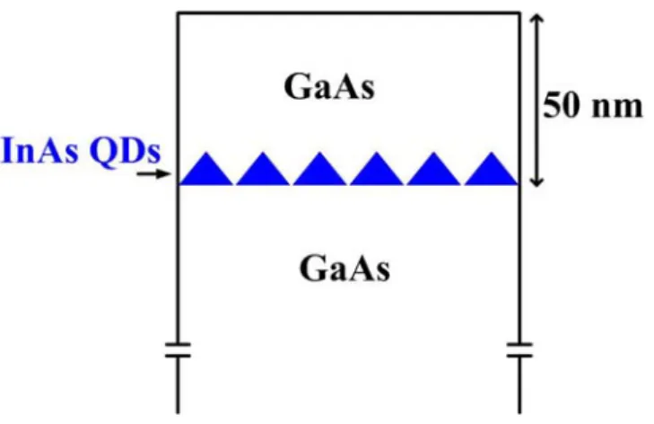
3.3 Sample structure and Measurement Condition
The samples of InAs QDs used in this study were grown by a molecular beam epitaxy (MBE) system. A buffer layer of 500 nm GaAs was grown first on a semi-insulating GaAs (100) substrate. Then InAs QD layers (each with 2.6 monolayers) was grown at a temperature of 520˚C. All samples were capped with a 50 nm thick GaAs layer. Arsenic pressure was 4–5×10⁻⁶ Torr. Growth rates were one μm/hr for GaAs and 0.056 μm/h for InAs. The InAs composition was influence by the growth rate of capped layer. Fig. 3.2 shows the schematic of the QDs samples.From the atomic force microscope (AFM) image, the density of QDs was determined to be approximately 1×1010 cm-2. RBS/w channeling measurement was performed by the 9SDH-2 Tandem accelerator at National Tsing Hua University. The beam divergence was less than 0.02°, defined by two sets of slits with 2.3 m apart. The ion beam current density was 200 nA/cm2 on the target. The sample was mounted on a three-axis goniometer with an angular resolution of less than 0.01°. Backscattered particles were collected by a PIPS detector at 160owith respect to the direction of the incident beam. The energy resolution of the system, determined by fitting the GaAs edge of the energy spectrum, was around 60 keV. This value is low enough to separate the surface peaks of Ga and As in the aligned spectrum (104 keV). To compliment the ion-channeling study, we also performed low-temperature (25 K) photoluminescence measurement using the 514.5 nm line of an argon ion laser. The signal was collected using a InGaAs detector and lock-in techniques.
FIG. 3.2. The structure of our samples. InAs QDs grown on the GaAs substrate. InAs QDs were embedded 50 nm below the surface.
3.4 Results of Angular Scan Curves
The angular scan of channeling experiment was performed along the [100] direction, which is normal to the sample surface, and the [110] direction, 45o to the surface normal direction. An angle scan for the [100] beam was performed along the(011)surface. Another angular scan was performed for the [110] direction beam along the (001) surface. In this way, we were able to probe the strain in the QDs in both the vertical and lateral directions. Fig. 3.3 shows schematically how the channeling beam probes a buried strain layer.
FIG.. 3.3. Schematic diagram of how a buried strained layer is probed by ion beam.
Backscattering spectrum shows the In and GaAs signal are separated completely. Figure 3.4 shows the angular scan curve, the curve provide strain information. In signal is the integral over the whole In peak In backscattering spectrum from 1200 to 1300 channel. GaAs signal is integral from 800 nm to 40nm channel.
FIG. 3.4. Backscattering spectrum shows the In and GaAs signal are separated completely. Tight figure shows the angular scan curve, the curve provide strain information. In signal is the integral over the whole In peak In backscattering spectrum from 1200 to 1300 channel. GaAs signal is integral from 800 nm to 40nm channel.
FIG. 3.5. Angular scan spectra along (a) [100] and (b) [110] axes of the as-grown QD sample. The angular shift was determined by the relative change in angle position of the half maximum of the In and Ga/As curves on either side of the channeling curves. From the sign of (∆θ)right -(∆θ)left, we determine which direction the
curves shift relative to each other. No obvious difference was observed between the curves of In and Ga/As in the [100] direction. In the [110] direction, we observe an angular shift of the In signal relative to the Ga/As signal toward the [100] direction.
We first looked at a sample with a single QD layer buried under a 50 nm GaAs cap. Fig. 3.5(a) and (b) show the angular scan of the In and the Ga/As signals for the as-grown sample along [100] and [110] directions. While the In signal is from the QDs and the wetting layer, the Ga/As signal was taken from the top 40 nm of the sample. The wetting layer is one monolayer and fully strained. The geometry of the wetting layer influences only the half width of the In angular scan (narrowing) and minimum yield for the [110] direction [38]. No significant difference was observed between the curves of In and Ga/As in the [100] direction. However, an angular shift was observed in the [110] scan, which indicates a lattice distortion in the buried QD layers. This is the first time that an angular shift was observed for samples with a buried strain QD layer.
The size of the dots, measured from TEM and AFM images, was about 4 nm in height and 20 nm in width. The calculated shadow cone length is 4 nm and 2.5 nm in the [100] and [110] directions, respectively. In [100] direction, because it is perpendicular to the strained layer, no angular shift in the angular scan can be obtained. Furthermore because the shadow cone length is about the same as the height of the QDs, according to the ion channeling theory [39], the In atoms in the QDs behave like In impurities in a GaAs matrix. The channeling behavior of the In signal from the QD layer is determined by the position of In atoms in the flux pattern emerged from the overlying GaAs capping layer. If the In atoms deviate from their equilibrium positions, they could cause the dip of the angular scan to be narrower. The fact that the angular scans of In and Ga/As are nearly identical indicates that there is no strain relaxation in the QDs in the lateral direction. For channeling along the [110] direction, because the shadow cone length is smaller than the QD size, it becomes possible to observe the lattice distortion directly from the shift of the angular scan spectrum. The angular shift was determined by the relative change in angle position of the half maximum of the In and Ga/As curves on either side of the channeling curves. From the sign of (∆θ)right -(∆θ)left, we
determine which direction the curves shift relative to each other.From Fig. 3.5(b), we indeed see a slight shift of the In signal relative to the Ga/As signal toward the [100] direction. This shift provides a directly evidence that the lattice of the InAs QDs is larger than that of the GaAs matrix in [100] or the crystal growth direction.
The effect of thermal annealing on strain relaxation in QDs was then studied. The as-grown sample was annealed at 650°C and 750°C for 30sec with a rapid thermal annealing furnace. The angular scan spectra after the sample was annealed at 650°C are shown in Fig. 3.6(a) and 3.6(b). In the [100] direction, we again did not see any difference between the In spectrum and the Ga/As spectrum. In the [110] direction, the angular shift of the In signal, however, becomes larger than that of the as-grown sample. So the InAs lattice remains the same in the lateral direction but becomes larger, less strained, in the growth direction after annealing. In other words, we start to see some strain relaxation in vertical direction.
The angular scan spectra of the sample annealed at 750°C are shown in Fig 3.7(a) and 3.7(b). The shape of the dip in the angular scans for the In signal in the [100] direction is clearly different from that of Ga/As. It has become narrower, which is a clear evidence of displaced In lattice. In the [110] direction, the angular scan spectra are similar to those of the sample annealed at 650°C. So annealing at 750°C caused the strain to relax not only in the vertical direction but also in the lateral direction. From these observations, we reach the following conclusion. The as-grown QDs have the same lattice constant as that of GaAs in the plane perpendicular to the growth direction. In the growth direction, the InAs lattice is larger than that of GaAs. After 650°C annealing, the InAs lattice of the QDs becomes larger or relaxed in the growth direction, but in the in-plane direction, the QDs remain strained with the lattice constant the same as that of GaAs. After 750°C annealing, however, the InAs lattice of the QDs not only relaxes in the growth direction but also becomes relaxed in the lateral direction.
FIG. 3.6. Angular scan spectra of the QDs annealed at 650oC. The In and Ga/As signal again match in the [100] direction. In the [110] direction, the angular shift of the In signal becomes larger than that of the as-grown sample.
FIG. 3.7. Angular scan spectra of the QDs annealed at 750oC. In the [100] direction, the In signal is narrower than that of the Ga/As signal. In the [110] direction, the angular scan spectra are similar to those of the sample annealed at 650°C.
3.5 The Strain State along Growth Direction
Therefore, from the channeling result, we know that the lattice constant of the InAs QDs is larger than that of GaAs in the vertical direction. However, whether they are under compressive strain or tensile strain is unknown. The effect of strain on the band gap energy of the QDs can be expressed as [43]
strain g unstrain QD g QD g E E E , = , , +Δ , (3.2)
where the strain induced band gap change, ΔEg ,strain, is expressed as
(
) (
)
(
)
[
]
2 ) ( 2 2 2 ,strain xx yy zz xx yy yy zz zz xx g E =α ε +ε +ε +β ε −ε + ε −ε + ε −ε Δ (3.3)The first term is the hydrostatic component and the second term the biaxial component. α and β, deformation potential coefficients of the hydrostatic and the biaxial components, are -6.08(α) and -1.8(β) for InAs. εij (i,j=x,y,z) are elements of the strain tensor. Since we have
seen that the in-plane lattice constant of InAs is the same as that of the GaAs matrix for the as-grown sample, the lateral strain components become
bulk InAs bulk InAs GaAs bulk InAs bulk InAs strain InAs yy xx a a a a a a , , , , , − = − = =ε ε (3.4)
Substituting in the lattice constants of GaAs and InAs, we obtain εxx=εyy = -0.067. Eq (3) is
then reduced to
ΔEg,strain =0.694−7.88εzz (3.5)
and the QDs band gap energy becomes
zz unstrain QD g QD g E E , = , , +0.694−7.88ε (3.6) The band gap energy of QDs, E , can be obtained from the photoluminescence
measurement. Fig. 3.11 shows the photoluminescence spectra of the QD sample before and after annealing. For the as-grown sample, Eg,QD,is determined to be 1.1eV. So the strain of the
QDs in the growth direction is
88 . 7 406 . 0 , , − = gQDunstrain zz E ε (3.7)
Since Eg,QD is lager than the bulk InAs band gap energy (0.416eV) because of the
quantum size effect, εzz must be positive. In other words, the QDs are tensile strained in the z
direction.
3.6 The Relationship between Optical properties and Strain State
The ion channeling results provide us with information on lattice distortion of the QDs before and after annealing. But they cannot tell us anything on the composition changes. The photoluminescence measurement, however, provides information on the band gap energy, which is influenced by both strain and composition.
The photoluminescence spectra shown in Fig 3.8 indicate that the emission peak of the QDs had a clear blue shift after the sample is annealed. This result, however, cannot be explained by the strain changes discussed above. From the channeling result, we know that annealing causes the strain of the QDs to relax, or the lattice to enlarge, first vertically then laterally. So the band gap should shrink after annealing. This should cause the photoluminescence emission to have a red shift. So the observed blue shift in the photoluminescence spectrum is obviously contrary to what is expected from the strain analysis. The reason for this discrepancy is attributed to the composition intermixing between the QDs and the surrounding GaAs during annealing as previously reported in [44]. The
intermixing obviously plays a bigger role than the strain effect in determining the photoluminescence emission spectrum when the QDs are annealed.
FIG. 3.8. Photoluminescence spectra at 25 K of QDs before and after annealing.
3.7 Conclusion
Ion channeling technique using MeV C++ ions was used to study strain in self-assembled InAs QDs buried in GaAs matrix. Because of the use of heaving ions, we were able to observe an angular shift in the angular scan of the In signal relative to that of the Ga/As signal. This provided a direct evidence that the InAs lattice is larger than that of GaAs in the growth direction. Combing the channeling results in [100] and [110] directions and the photoluminescence emission spectrum, we conclude that the InAs QDs are under tensile strain in the growth direction and have the same lattice constant as that of GaAs in the lateral direction. Thermal annealing causes the strain to relax, first in the growth direction and then
in the lateral direction as the annealing temperature increases. The photoluminescence spectra of the QDs before and after annealing indicate, however, that composition intermixing also takes place during annealing and is the dominant factor in determining the band gap energy of the QDs.
Chapter 4
The wavelength switching Transition in quantum dots lasers
4.1 Introduction
InAs self-assembled quantum dots (QDs) generally exhibit two distinct peaks in photoluminescence spectra corresponding to the ground and the excited state transitions. It is of great interest that whether these two transitions can have properties of the two distinct state lasing, which may be one important development in the laser research. The possibility of two-state lasing had been demonstrated in theory by Grundmann et al [45-46]. Simultaneous lasing at two well-separated wavelengths has been experimentally shown in self-assembled InAs QD lasers via ground state and excited state transitions [47-49]. However, the possibility of lasing switching between two wavelengths has not been completely studied. In this chapter, we present a detailed lasing switching behavior between the ground state and the excited state in InAs QD lasers. The lasing switching behavior is presented in two parts: (1) convention single cavity laser; (2) couple cavity laser system.
4.2 Device Growth
The QD lasers were grown on (100)-n+ GaAs substrates using molecular beam epitaxy (MBE). The epi-layer structures of the lasers consisted of, starting from the bottom, a 1.2 μm
1.2 mm n-Cladding Al0.6Ga0.4As
50 nm Al0.6Ga0.4As─Al0.2Ga0.8As
GaAs
50 nm Al0.6Ga0.4As─Al0.2Ga0.8As 1.2 mm p-Cladding Al0.6Ga0.4As
p+ Contact Layer GaAs
GaAs 3 QDs Layers with 6 nm In0.15Ga0.85As cap 1.2 mm n-Cladding Al0.6Ga0.4As 50 nm Al0.6Ga0.4As─Al0.2Ga0.8As GaAs 50 nm Al0.6Ga0.4As─Al0.2Ga0.8As 1.2 mm p-Cladding Al0.6Ga0.4As
p+ Contact Layer GaAs
GaAs
3 QDs Layers with 6 nm In0.15Ga0.85As cap
FIG. 4.1. The growth sequence of laser is schematically shown. The hetero-structure for QDs were grown by MBE.
thick n-type Al0.4Ga0.6As cladding layer with 3x1017 cm-3 Si doping, a 0.4 μm thick undoped
GaAs waveguide layer, a 1.2 μm-thick p-type Al0.4Ga0.6As upper cladding layer with 3x10¹⁷
cm-3 Be doping, and finally a 200 nm-thick p+ GaAs contact layer. The active region consists of three InAs QD layers, which reside in the middle of the waveguide layer. Each QD layer is capped by a 6 nm In0.15Ga0.85As layer. A 40-nm GaAs barrier layer is inserted between the
QD layers. In growth rate for QDs and capping layer is 0.056 μm/hr. The layer structure of the laser is schematically shown in Fig. 4.1.
4.3 Device Process
Conventional ridge waveguide structure was used for QDs laser fabrication. The cavity width is 20 μm. The cavity lengths are varied from 1000 to 1500 μm. Typically, the laser devices studied in this dissertation were processed with a standard procedure. To confine optical field in lateral direction, shallow mesa was necessary. First, the desired device patterns were processed by standard photo-lithography steps. That is, photo-resist coating, soft baking, exposure under UV light, development in developer solution, rinse in DI water and dry by pure nitrogen purge. After photo-lithography steps, p-type ohmic contacts of Ti/Pt/Au were deposited. All metal contacts were formed by E-gun evaporation, the chamber pressure was lower than 2x10⁻⁶torr. Before metal formation, the surface was treated with the following steps. First, to remove residue photo-resist, the surface was treated with UV/O3 stripper at temperature of 100oC for 2 minutes. The native oxide on the surface was etched by using the solution of HCl: H2O (1:1) for 30 seconds. After native oxide removal, the wafers were rinsed
in DI water and then dried by pure nitrogen. In order to prevent from re-oxidation of the surface in the air, the wafer was loaded into the E-gun chamber quickly after surface treatment. When the wafers were unloaded from E-gun evaporation, Lift-off in acetone (ACE) could made the p-contacts strip patterns appear.
The shallow mesa of the ridge lasers were formed by using wet chemical etching. In details, solution of H2SO4: H2O2: H2O (1:8:40) with an etching rate of about 20 nm/s was used for
mesa formation. All etching process was carried out at room temperature. For all conventional ridge waveguide structure, whether the lasers were single or couple cavity, etching stop in the interface between p-cladding and GaAs waveguide.
The metal alloy in n-ohmic contacts were different from the p-ohmic contacts, therefore, n-contacts were formed after the shallow mesa formation. To cleave lasers cavity with different length, the wafers should remove their thickness on substrate side before depositing
n-metal alloy. Generally, the 200 μm thick n-substrate should be removed with chemical wet-etching solution (NH3OH:H2O2=1:3). Ni/Ge/Au n-contacts were formed by E-gun
evaporation; the chamber pressure was also lower than 2x10⁻⁶torr. Before n-metal formation, the surface was also treated for removing native oxide. The steps had been expressed above. The rapid thermal annealing (RTA) step was performed after n-metal contact formation. The n-metal contact becomes ohmic contact after the RTA step. RTA temperature is 400oC for 30 second. Figure 4.2 shows the fabrication procedure of our lasers.
P-contact pattern Photo lithography Coating Photo-resist P-metal deposit P-contact pattern Photo lithography Coating Photo-resist P-metal deposit Lit-Off mesa formation with wet etching
Substrate thin-down and N-metal contact
Lit-Off
mesa formation with wet etching
Substrate thin-down and N-metal contact
FIG.4.2. The conventional ridge waveguide structure was fabricated with standard procedure.
4.4 Characteristic Measurement System
Laser light- current (L-I) measurements were performed under pulsed condition. The pulsed currents were generated by as HP8114A pulsed generator. The light output is detected by a calibrated Si or InGaAs PD with 9 volts reverse-biased. The injection current and the detection current are then gated and integrated by the Standford research system SR250 gated integrator and boxcar averager. In our experiment, the pulse width was 1 μs and the duty cycle was 5%. Fig. 4.3 shows the schematic of the L-I measurement system. The spectra of the quantum dot lasers were measured by an optical analyzer. The lasers were characterized in the temperature range of 20-60 oC.
4.5 Lasing switching in single cavity QD lasers
4.5.1 Using Different Drive Currents
Fig. 4.4 (a) and (b) show the output power and lasing spectra of an as-cleaved OD laser at different drive currents. The cavity width and length were 20 μm and 1400 μm, respectively. The laser was operated at 20°C. In Fig.4.4 (a), the L-I curve reveals that the ground state threshold is 44 mA. With increasing injected current, we observe that the slope of L-I curve changes at certain point. The lasing spectra at different driving currents have also been measured. The results are shown in Fig 4.4(b). The ground state transition appears around 1.23 μm at 44 mA. The output power of the ground state emission saturated with bias current at 120mA.With increased drive current to around 130mA, an additional spectral band appears around 1.124 μm, which corresponds to the wavelength of the first excited state transition. Between 130 mA and 190 mA, both the ground state band and the excited state band exist together. By comparing with the results in Fig.4.4(a), the change of the slope in L-I curve occurs at the point that the output power of the ground state emission saturated and the excited state lasing starts to take place. When the higher current I s used, the output power of the ground state lasing gradually disappears. Finally, the lasing completely switches from the ground state transition to the excited state transition.
In conclusion, the lasing wavelength of QD lasers depends on the driving current. The ground state lases first, followed by the excited state. Then, two-state lasing occurs. Finally, lasing wavelength switches to the excited state transition. The change of slope in L-I curve indicates that the ground state power saturated and the excited state lasing threshold reaches.
(a)
(b)
FIG. 4.4. The results L-I curve of QDs laser and the optical spectrum with varied bias currents, respectively. In the QDs laser, cavity width is 20 μm and cavity length is 1.4 mm.
4.5.2 Cavity Length and Operation Temperature
The L-I curves of QD lasers with various cavity lengths and operation temperatures are depicted in Fig. 4.5(a)-(e), where show mode switching for the cavity length varied from 1100 (Fig. 4.5(a)) to 1500 μm (Fig. 4.5(e)) with a step 100 μm and at various temperatures (20-40°C). Optical output power spectra are also monitored simultaneously, but the results do not show here. Fig. 4.5(a) shows that lasing threshold occurs at 80mA. Combined with the results of optical output spectra, we find that the laser only lases at the excited state transition. At such cavity length (i.e. 1100μm), the gain from the ground state transition is too small to compensate for the total loss. Fig. 4.5(b) represents the L-I curves of the 1200 μm long laser. At 20°C, a lasing threshold occurs at lower current than that in 1100 μm length laser (Fig. 4.5(a)). The slop of L-I curve changed at higher driving currents. The corresponding optical output power spectrum indicates that the lasing starts with the ground state transition. The excited state lasing starts at where the slope of L-I curve changes. When the temperature is raised to 25°C, only excited state lasing is observed.
Three L-I curves with three different temperatures (20°C, 25°C, 30°C) and the same laser cavity length (1300 μm) are shown in Fig.4.5(c). The ground state threshold occurs at 20 and 25°C operation temperature. At 30°C operation temperature, lasing changes from the ground state transition to the excited state transition. The wavelength switching between these two transitions occur at higher temperature. The change of the slope appears at lower current as the operation temperature increased. It indicates that the excited state threshold decreases with higher operation temperature. Fig. 4.5(d) and (e) show results at five different temperatures for cavity length at 1400 and 1500 μm, respectively. These results are similar to those in Fig. 4.5(c). The ground state (excited state) threshold increases (decreases) with increasing the operation temperature. When the temperature is higher than a certain temperature, only excited state lasing is observed. This certain temperature increases when

![FIG. 2.5. The measured Si (substrate) and SiGe (strained epi-layer) angular scans of the [111] axis](https://thumb-ap.123doks.com/thumbv2/9libinfo/8624173.191770/31.892.131.749.112.433/fig-measured-substrate-sige-strained-layer-angular-scans.webp)
![FIG. 3.1. Calculated result of close-encounter probability of C ++ (dot line) and He + (solid line) ions impinging on a [100] GaAs surface versus the depth from surface](https://thumb-ap.123doks.com/thumbv2/9libinfo/8624173.191770/37.892.129.763.528.1049/calculated-result-encounter-probability-impinging-surface-versus-surface.webp)
![FIG. 3.5. Angular scan spectra along (a) [100] and (b) [110] axes of the as-grown QD sample](https://thumb-ap.123doks.com/thumbv2/9libinfo/8624173.191770/41.892.267.671.110.850/fig-angular-scan-spectra-axes-grown-qd-sample.webp)
