國立交通大學
光電工程研究所
碩士學位論文
矽基板上矽奈米柱的形成與特性分析
Characteristics of Si nanopillars
Formatted on Si Substrate
研 究 生:林皇伸
指導教授:林恭如 教授
郭浩中 教授
中 華 民 國 九 十 五 年 七 月
光電工程研究所 國立交通大學 編號 : 碩 士 論 文
矽奈米柱在矽基板上的形成與特性
分析
研究生:林皇伸矽奈米柱在矽基板上的形成與特性分析
Characteristics of Si nanopillars Formatted on Si Substrate
研 究 生:林皇伸 Student:Huang-Shen Lin
指導教授:林恭如 Advisor:Gong-Ru Lin
郭浩中 Hao-Chung Kuo
國 立 交 通 大 學
光 電 工 程 研 究 所
碩 士 論 文
A ThesisSubmitted to Institute of Electronics College of Engineering National Chiao Tung University
in partial Fulfillment of the Requirements for the Degree of
Master
In Electro-Optical Engineering
June 2006
Hsinchu, Taiwan, Republic of China
博碩士論文電子檔案上網授權書
本授權書所授權之論文為授權人在 國立交通 大學(學院) 光電工程
系所_______組 九十四 學年度第 二 學期取得 碩 士學位之論文。
論文題目:矽奈米柱在矽基板上的形成與特性分析
指導教授:林恭如 與 郭浩中老師
茲同意將授權人擁有著作權之上列論文全文(含摘要),非專屬、無償
授權國家圖書館,不限地域、時間與次數,以微縮、光碟或其他各種
數位化方式將上列論文重製,並得將數位化之上列論文及論文電子檔
以上載網路方式,提供讀者基於個人非營利性質之線上檢索、閱覽,
或並下載、列印。
□讀者基於非營利性質之線上檢索、閱覽或下載、列印上開論文,應依著 作權法相關規定辦理。指導教授:
林恭如 & 郭浩中教授 授 權 人 研究生姓名: (請親筆正楷簽名)中 華 民 國 九十五 年 月 日
博碩士論文授權書
本授權書所授權之論文為本人在國立交通大學(學院)光電工程系所______組_ 九十四_學年度第_二_學期取得_碩_士學位之論文。 論文名稱:矽奈米柱在矽基板上的形成與特性分析
同意 □不同意 (政府機關重製上網) 本人具有著作財產權之論文全文資料,授予行政院國家科學委員會科學技術 資料中心、國家圖書館及本人畢業學校圖書館,得不限地域、時間與次數以 微縮、光碟或數位化等各種方式重製後散布發行或上載網路。 本論文為本人向經濟部智慧財產局申請專利(未申請者本條款請不予理會) 的附件之一,申請文號為:______,註明文號者請將全文資料延後半 年再公開。 --- □同意 □不同意 (圖書館影印) 本人具有著作財產權之論文全文資料,授予教育部指定送繳之圖書館及本人 畢業學校圖書館,為學術研究之目的以各種方法重製,或為上述目的再授權 他人以各種方法重製,不限地域與時間,惟每人以一份為限。 上述授權內容均無須訂立讓與及授權契約書。依本授權之發行權為非專屬性發行權 利。依本授權所為之收錄、重製、發行及學術研發利用均為無償。上述同意與不同意之 欄位若未鉤選,本人同意視同授權。 指導教授姓名:林恭如 研究生簽名: 學號:9324526 (親筆正楷) (務必填寫) 日期:民國 年 月 日 1. 本授權書 (得自 http://sticnet.stic.gov.tw/sticweb/html/theses/authorize.html 下載) 請以黑筆撰寫並 影印裝訂於書名頁之次頁。 2. 授權第一項者,請確認學校是否代收,若無者,請個別再寄論文一本至台北市(106-36)和平東 路二段 106 號 1702 室 國科會科學技術資料中心 王淑貞。(本授權書諮詢電話:02-27377746) 3. 本授權書於民國 85 年 4 月 10 日送請內政部著作權委員會(現為經濟部智慧財產局)修正定稿, 89.11.21 部份修正。 本案依據教育部國家圖書館 85.4.19 台(85)圖編字第 712 號函辦理摘 要
論文名稱: 矽基板上矽奈米針的形成與特性分析 校所別:國立交通大學光電工程研究所 頁數:2 頁 畢業時間:九十四學年度第二學期 學位:碩士 研究生:林皇伸 指導教授:林恭如 郭浩中老師 關鍵詞: 矽、奈米針、自我凝聚、鎳、活化性離子蝕刻、光激發、奈米、光性、 反射率、量子侷限 在本論文中,我們成功地利用二氧化矽薄膜當緩衝層,使得鎳的奈米顆 粒成功地快速凝聚在矽的基板上。因為矽的高熱導 148 W/m-K 造成熱快速散 逸,所以奈米鎳顆粒很難直接地聚集在矽的基板上。藉由厚度 200 Å 且熱導只 有 1.35 W/m-K 的二氧化矽當緩衝層,阻止了 NiSi2化合物的產生,和讓奈米鎳 顆粒因為在鎳和矽界面之間吸附力減小與熱的累積,更容易形成自我凝聚。 因此,奈米鎳顆粒可以加速形成,退火時間大大縮短到 22 秒。奈米顆粒的大 小和密度平均是 30 奈米和 7×1010 cm-2 。利用鎳在二氧化矽層上自我凝聚成的奈 米粒當奈米遮罩,經過活化離子式蝕刻後,可以在矽的基板上製造出大面積的矽 奈米針陣列,而針的大小可以被控制到小於 50 奈米。在我們的實驗中,矽奈米 針的最理想高寬比是 8。此時,針的平均大小和高度分別是 40 奈米和 400 奈米。 去除掉在矽的基板上的奈米粒和二氧化矽後,從矽奈米柱發出的光激發可以發現 到 400 到 600 奈米的可見波段和 750 奈米的近遠紅外波段。400 奈米到 600 奈米 的可見波段主要源自於氧的弱鍵結(WOB)、中性的氧化缺陷(NOV)與 E'缺陷。 更進一步地,因為矽奈米針持續氧化產生在光激發譜上的藍位移現象和產生在變 功率光激發譜上的強度飽和現象,所以成功地證實 750 奈米波段是量子侷限效應。其他在電性上,相較於矽的靶材,矽奈米針擁有較快的充放電速度、較低的 電阻和超低漏電流,而在光性,則明顯有較低的反射率。
ABSTRACT
Title:Characteristics of Si nanopillars Formatted on Si Substrate Pages: 2 Pages
School:National Chiao Tung University
Department:Institute of Electro-Optical Engineering
Time:June, 2006 Degree:Master
Researcher:Huang-Shen Lin Advisor:Prof. Gong-Ru Lin Prof. Hao-Chang Kuo
Keywords : Si 、 nanopillar 、 self-assemble 、 Ni 、 reactive ion etching 、 photoluminescence、nano、optical、reflective ratio
In this essay, rapid self-aggregation of Ni nanodots on Si substrate covered with a thin SiO2 buffered layer is investigated. Ni nanodots are hard to self-aggregate on highly heat dissipated Si substrate with a thermal conductivity of 148 W/m-K. Adding 200Å-thick SiO2 buffer with an ultralow thermal conductivity of 1.35 W/m-K prevents the formation of NiSi2 compounds, facilitates the self-assembly of Ni nanodots from enhanced heat accumulation and released Ni adhesion with Si. Formation of Ni nanodots can therefore be accelerated with size and density of 30 nm and 7×1010 cm-2, respectively, under an annealing time greatly shortened to 22 sec. With the advantage of the self-assemble Ni/SiO2 nano-dots based nano-mask, a large-area Si nano-pillar array with rod size of <50 nm can be formatted on Si substrate through the induced coupled plasma reactive ion etching (ICP-RIE) procedure. In our experiment, the optimum aspect ratio of the Si nanopillars is 8 with the average diameter of 40 nm and the average height of 400 nm. After removing Ni dots and the SiO2 film on the Si substrate, both the visible 400 nm-600 nm and near infrared 750nm photoluminescence from the Si nano-pillar sample were observed and analyzed. The visible emission 400 nm to 600 nm mainly originated from the weak oxygen bond
(WOB) the neutral oxygen vacancy (NOV) defects, and the E’ defects. Moreover, the peak wavelength of 750 nm is emitted from the quantum confining centers proven by the blue shift of the oxidizing Si nanopillars in the μPL and the saturating peak intensity in the power dependentμPL. Comparing to the bulk structure, the Si nanopillars owned the high charging and discharging speed、low resisters and no leakage current in electrics and the low reflectance in optics.
ACKNOWLEDGEMENT
碩士班二年的學習讓我獲益良多,首先我要感謝我的指導教授林恭如老 師和郭浩中老師,每當我的實驗陷入困境時,老師都會給我加油打氣並指引 我方向,讓我的論文成功地被國際期刊接受,還帶我出席國際會議增廣見識, 可見老師對學生的關心與用心栽培。接著,我要感謝林俊榮學長和高志強學 長,跟學長的討論總是讓我對半導體製程和原理的了解更清楚,也謝謝學長 們長期對我在實驗上的幫忙,我特別地感謝半導體實驗室的同學們對我的幫 忙,謝謝姚析宏學長教我 AFM,謝謝賴俊峰學長教我 micro PL,謝謝葉剛帆 同學教我鍍金屬和 RTA,謝謝游敏同學教我 PL,謝謝高宗鼎同學和林立凡學 弟幫我照 SEM,謝謝我的麻吉許意偵同學教我電性量測,謝謝大家在我心情不 好的時候陪我唱歌,謝謝王興宗老師的充電之旅和中秋烤肉,最後我要感謝 大家二年來的陪伴與照顧。CONTENTS
Page
Abstract (in Chinese)
iAbstract (in English)
iiiAcknowledgement
vContents
viList of Figures
viiiChapter 1 :
Introduction1.1 Review of Metallic Mask 1 1.2 Formation of Si Nanopillars 2 1.3 Photoluminescence of Si Nanopillar 2
1.4 Motivation 4
1.5 Structures of the essay 4
1.6 References 5
Chapter 2 :
Study of Ni Self-assembly2.1 Introduction 8
2.2 SiO2 Thickness 10
2.3 Annealing Temperature and period 11
2.4 Ni thickness 16
2.5 Conclusion 17
2.6 References 18
Chapter 3 :
Formation of Si Nanopillars3.1 Introduction 20
3.2 Experimental Process 21 3.3 Results & Discussions 22
3.3-1 Gas Flowing 22 3.3-2 Chamber Pressure 24 3.3-3 Etching Power 25 3.3-4 Etching Time 30 3.4 Conclusion 31 3.5 References 32
Chapter 4 :
Optical and Electrical Characteristics of Si nanopillars
4.1 Introduction 34
4.2.1 Experimental 35 4.2.2 Structure Damage Dependent PL 37
4.3 Reflection 41
4.4 Current-Voltage and Capacitance-Voltage Curve 43
4.5 Conclusions 49 4.6 References 50
Chapter 5 :
Summary 5.1 Summary 52 Curriculum Vitae 54 Publication list 55LIST OF FIGURES
Fig2.1 Self-aggregation of Ni nanodots on Si substrates without or with SiO2 buffered layer of different thickness.
Fig2.2 SEM images of Ni nanodots after annealing for 30s and 120s at 850℃ shown in 2.2(a) and 2.2(b). Apparently the density of dots for
shorterer annealing time is denser by comparing the plots in 2.2(c).
Fig2.3 The size and density of Ni dots as a function of the annealing time when the thickness of SiO2 is 200Å. The 22 sec annealing time at 850℃ is
the optimum item for the densest density and the smallest diameter.
Fig2.4 The size and density of self-aggregated Ni nanodot as a function of annealing time.
Fig2.5 SEM images of Ni dots after different annealing temperature for 120s. Apparently the density of dots at lower annealing temperature is denser.
Fig2.6 SEM images of Ni dots formed from different thick Ni layer at 850 oC for 120 s. Apparently, the density of dots with the thinner deposition of Ni layer is denser.
Fig3.1 Schematic illustration of Si nano-pillar arrays using Ni/SiO2 as
nano-masks formation. The reaction products after RTA and ICP-RIE etching, leading to the formation of Si nano-pillar arrays.
Fig3.2 The SEM images of Si nanopillars formed under three different flowing of etching gas CF4
Fig3.3 The SEM images of Si nanopillars formed under four different flowing of etching gas Ar.
Fig3.4 The SEM images of Si nanopillar formed at three different etching pressures.
Fig3.5 (a) shows the apparently triangle shape of Si nano-pillar. (b) The sharper sidewall of Si nanopillar. (c) A sharp side-wall of Si pillar with insufficient height.
Fig3.6 Different ratio of ICP power over bias power has different influence on the vertical level of Si pillars’ side-wall.
Fig3.7 The different magnitude of power with the same ratio of bias and ICP power.
Fig3.8 The cross section SEM images of the Si nanopillars were formed at the different RF power from 50 W to 200 W
Fig3.9 The cross section SEM images of the Si nanopillars were formed at the different bias power from 0 W to 75 W.
Fig3.10 The cross section SEM images of Si nanopillars were etched for different time from 3 min to 9 min.
Fig4.1 The PL measurement is set up with the 325nm He-Cd laser、a pair of mirrors and focal Lenses、a beam splitter、a Triax320 spectrometer、 photonic multiplying tube.
Fig4.2 (a) SEM image of Si nano-pillars after removing the Ni and SiO2 l ayers at the etching-power ratio of 2 for 3 min. (b) AFM data including 3-D 45°view angle image and the height profile. (c)
Photoluminescence of Si nano-pillars in (a) and decomposed by two Gaussion fits at 418 and 451 nm.
Fig4.3 (a) Photoluminescence of Si nano-pillars for different pumping power densities. (b) Peak intensity for different pumping power densities.
Fig4.4 The experimental setup contains the confocal microscopy and
micro-photoluminescence (μ-PL) system that can focus the laser beam to 1μm.
Fig4.5 Power dependent photoluminescence of Si nanopillar array pumped by 325 nm HeCd laser and detected by PMT. The inset is the peak
intensity of 750 nm under the various pumping power density. From the inset, the saturation of the peak is observed.
Fig4.6 The different reflectance comes from different Si structures inclusive of bulk、capped with Ni and SiO2 layer、Ni dots formed after RTA、 Si pillars capped with Ni and SiO2、pure Si nanopillar array.
Fig4.7 The reflections of Si substrate were measured from the 20 degree to 89 degree. The pR stands for p-polarization (TM mode);the sR stands for s-polarization;the uR stands for circle- -polarization.
Fig4.8 The comparing I-V curves of different Si structures includes bulk、Ni layer on Si、Ni dots on Si、Si nanopillars with Ni caps、pure Si nanopillars.
Fig4.9 Fig 4.9 (A) The capacitance under different gate voltage. (B) Energy band diagrams and charge distributions of an ideal MOS diode in (B)-(a) accumulation, (B)-(b) depletion, and (B)-(c) inversion.
Fig4.10 Effect of a sheet charge within the oxide. (A)-(a) Condition for VG = 0. (A)-(b) Flat-band condition. Effect of a oxide charge and interface
traps on the C-V characteristics of an MOS diode.
Fig4.11 The C-V curves are measured from Si bulk and Si nanopillar array.
CHAPTER 1
Introduction
1.1 Review of Metallic Mask
In order to produce Si nanopillar array, the E-beam lithography was the most common way to fabricate the nano mask. However, the process of the E-beam lithography is high cost and low efficiency. Nowadays, the metallic nanodot arrays such as Au、Al、Ni or Ag [1.1-1.4] have been extensively used as nanoscale masks to fabricate quantum confined Si nanodots, or been employed in resonant surface-plasma-wave based bio-photonic sensing applications. In particular, the self-assembly of Ni nanodots has also caused researching interests due to its potential applications in field-emission and bio-magnetic sensing. Previously, Lee et al. [1.2] employed the Ni nanodot mask with diameter and density of about 41 nm and 5.3×109 cm-2 to form Si nanorods. However, the disadvantage is that the self-aggregation of the Ni nanodots from Ni film coated on Si substrate usually takes up to 10 min even by rapid thermal annealing (RTA) process at 700oC in N2 ambient. It was mentioned in previous experiment that the self-aggregation of evaporated Ni film on pure Si wafer is hard to initiate without long-term annealing process, and the density of the formatted Ni nanodots is too sparse for applications. Such a long-term annealing inevitably leads to an unintentional doping or diffusion of the coated Ni into Si substrate during self-assembly procedure. On account of the larger thermal conductivity, the Si substrate that reduces the heat accumulating on the interface of Ni and Si, and the self-aggregating speed is slowed down due to the relatively good adhesion between the Ni and Si interface. It is noticed that the thin nitride layer such as Si3N4 [1.3] or TiN [1.5-1.6] layers could prevent the formation of NiSi2 compounds [1.7] and retain the thermal power on the Si surface. In this essay, we propose for the first time the quick
formation of Ni nanodots on Si substrate covered with a thin buffered SiO2 layer because the insufficient heat accumulation and strong adhesive problems happened at the Ni/Si interface can be solved by depositing a thin layer of SiO2 on Si substrate prior to the Ni evaporation and RTA processes.
1.2 Formation of Si nanopillars
The Si nano-pillar array has been shown to have the potential for many applications such as being photonic crystals [1.8], data storage [1.9], field electron emitter [1.10], nanoscale transistors [1.11-1.12] and light emitting devices [1.13]. The reactive ion etching [1.14] and thermal growth with the catalyst [1.15] were employed as two major procedures to obtain Si nano-pillar array with the aid of self-assembled metal nano-dot mask patterns such as Au、Ag or Ni. However, the diameter and the growing direction of Si nanowires are hard under the control. The etching procedure is the only choice to form not only straight but also thin Si one dimension structures. With the novel approach, the formation of the Si nanopillar array can be mostly realized by the induced coupling plasma reactive ion etching (ICP-RIE) of oxide-covered Si substrate capped with the mask of self-assembled Ni nanodots. Yoo et al. have made use of Ni nano-dot mask to form Si nano-pillars with diameter and height of about 41nm and 472nm, respectively. Nevertheless, the disadvantage of their results is that the density is too sparse to enhance the luminescence, and the self-aggregation of the Ni nano-dot from a Ni film coated on a Si substrate usually takes up to 10 min even by a rapid thermal annealing (RTA) process at 700oC in the N2 ambient [1.2]. The
1.3 Photoluminescence of Si Nanopillars
have extended by the construction of one-dimension silicon structures. [1.16-1.20] Theoretical studies of realized Si quantum wires confirm that there is a transition from the indirect to a direct gap material in Si, induced by electron confinement in nanostructures. [1.21-1.23] The theoretical result may be tested by the fabrication of well controlled and ordered nanostructures which are expected to give luminescence too, if the theoretical results are valid. The fabrication of this type of nanostructure presents the additional interest that they are produced by technology, so an additional step is made towards Si based optoelectronic devices, integrated on the same substructure with the microelectronic circuit. Early in 1996, Nassiopoulos et al. has been invented the electroluminescent device based on Si nanopillars. [1.24] The Light emission in the visible range was observed in forward bias when the voltage exceeded 12–14 V. The characteristics of this EL signal were similar to the PL signal observed from the same sample. A mechanism of EL emission related to high electric field electronic transport through the wires is suggested. In 1998, Papadimitriou et al. also fabricated highly anisotropic Si nanopillar array with the aspect ratio 25:1 and the diameters <100 nm by lithography and etching and also by several cycles of thermal oxidation and oxide removal by HF dip.[1.25] The anisotropic Si nanopillar array emitted photoluminescence in the range of 500-600nm. Moreover, the photoluminescence efficiency and energy position depended on the wavelength and the polarization state of the initial laser beam. This dependence was explained as originating from quantum confinement effects. In 2004, Yanagiya et al. tired to grow Si nanowires on sapphire with the width 50nm and the height 1nm by using disilane (Si2H6) gas-source molecular beam epitaxy (MBE). [1.26] The visible photoluminescence from the Si quantum wires was observed at the peak wavelength 750nm at 9 and 300 K. However, the PL intensity at 9 K is over 20 times larger than that of 300 K and the PL emission peak barely shifts between 9 and 300 K.
1.4 Motivation
The main motivation in our experiment is to form dense Si nanopillars with high aspect ratio on Si substrate and to research the most appealing topic----the Si emission. Instead of the e-beam or lithographic techniques, the sample and cheap way was realized by using the self-assembled metal dots. From section 1.1, it was obvious that many metals can congregate to dot form after annealing such as Au、Al、Ag、Ni and so on. We took advantage of Ni dots as our mask for its hardness and low cost comparing to Au、Ag and Al during the etching process. In 2005, proposed by Lee et al. [1.2], Ni nanodot array was utilized as a mask and the Si nanopillar array was manufactured successfully. However, the process of Ni dot formation took 10 min that was a long period and the density of the Ni dots wasn’t dense enough. Since the diameter and density of Si nanopillars are both controlled by ones of the Ni nanodots, we investigated a special way to fabricate the dense and small Ni nanodots without taking long period. By consulting the method in ref. 1.4, we inserted the buffer layer of SiO2 between the Ni film and Si substrate.
1.5 Structures of this essay
The main topics of this essay are the formation of the Ni nanodots、the process of the Si nanopillar array、the optics and electrics of the Si nanopillars that separately are discussed in chapter2、chapter3 and chapter4. In chapter2, we will study how to achieve the dense and small-sized Ni dots aggregated on Si substrate inclusive the impacts of annealing temperature、annealing time、Ni thickness and the most weighty buffer layer----SiO2. In chapter3, we will debate the conditions for getting Si nanopillars with the high aspect ratio including the discussion of the etchant gas flowing、pressure、
power and time. After the manufacture of the Si nanopillars, the following mission is to make a understanding of it in the optical and electrical aspects that is arranged in chapter4. Depending on these special characteristics of Si nanopillars, we must be able to improve the medical or communicating technologies such as bio-sensors、emitters or memory and then rich our life.
1.6 Reference
[1.1]
Y. Homma, P. Finnie, T. Ogino, H. Noda, and T. Urisu, J. Appl. Phys. 86, 3083 (1999).
[1.2] D. Crouse, A. Y.-H. Lo, E. Millar, and M. Crouse, Appl. Phys. Lett. 76, 49 (2000).
[1.3] J. S. Lee, S. K. Kim, G. Y. Yeom, J. B. Yoo, and C. Y. Park, Thin Solid Films 475, 41 (2005).
[1.4] H. W. Huang, C. C. Kao, T. H. Hsueh, C. C. Yu, C. F. Lin, J. T. Chu, H. C. Kuo, and S. C. Wang, Mat. Science & Eng. B 113, 125 (2004).
[1.5] J. Narayan and S. Oktyabrysky, J. Appl. Phys. 92, 7122 (2002). [1.6] J. Narayan and B. C. Larson, J. Appl. Phys. 93, 278 (2003).
[1.7] H. Zhou, D. Kumar, A. Kvit, A. Tiwari, and J. Narayan, J. Appl. Phys. 94, 4841 (2003).
[1.8] V. Poborchii, T. Tada, and T. Kanayama, Opt. Commun. 210, 285 (2002). [1.9] K. Sunouchi, H. Tkato, N. Okabe, T. Yamada,T. Ozaki, S. Inoue, K.
Hashimoto, K. Hieda, A. Nitayama, F. Horiguchi, and F. Masuoka, in IEDM Tech. Dig. 23 (1989).
[1.10] A. V. Karabutov, V. D. Frolov, A. V. Smakin, and G. A. Shafeev, IEEE Proceedings of the 14th International Vacuum Microelectronics Conference
(IVMC2001) 115 (2001).
[1.11] M. Terauchi, N. Shigyo, A. Nitayama, and F. Horiguchi, IEEE Trans. Electron. Dev. 44, 2303, (1997).
[1.12] F. D. Bauer, Solid-State Electron. 48, 705 (2004).
[1.13] A. G. Nassiopoulos, S. Grigoropoulos, and D. Papadimitriou , Appl. Phys. Lett. 69, 2267 (1996).
[1.14] C. W. Kuo, J. Y. Shiu and P. Chen, Chem. Mater. 15, 2917 (2003)
[1.15] S. H. Xu, Z. H. Xiong, L. L. Gu, Y. Liu, X. M. Ding, J. Zi and X.Y. Hou, Appl. Phys. A 76, 589 (2003).
[1.16] H. I. Liu, N. I. Maluf, R. F. Peace, D. K. Biegelsen, N. M. Johnson, and F. A. Ponce, J. Vac. Sci. Technol. B 10, 2846 (1992).
[1.17] A. G. Nassiopoulos, S. Grigorpoulos, D. Papadimitriou, and E. Gogolies, Appl. Phys. Lett. 66, 1114 (1995).
[1.18] S. Grigorpoulos, E. Gogolies,A. D. Tserepi, and A. G. Nassiopoulos, J. Vac. Sci. Thechnol. B 15, 640 (1997).
[1.19] J. Westwater, D. P. Gossian, S. Tomiya,Y. Hirano, and S. Usui, Mater. Res. Bull. 452, 237 (1997).
[1.20] A. S. Chu, S. H. Zaidi, and S. R. J. Brueck, Appl. Phys. Lett. 60, 905 (1993). [1.21] N. T. Bagraev, E. I. Chaikina, L. E. Klyachkin, I. I. Markov, and W. Gehlhoff,
Superlattic. & Microstruture 23, 337 (1998).
[1.22] S. Horiguchi, Superlattice & Microstructure 23, 355 (1998).
[1.23] Y. Zheng, C. Rivas, R. Lake, and T. B. Boykin, IEEE Trans. on Electron Devices. 52, 1097 (2005).
[1.24] A. G. Nassiopoulos, S. Grigoropoulos and D. Papadimitriou, Appl. Phys. Lett.
69, 2267 (1996).
[1.26] S. I. Yanagiya, M. Matsui, M. Yoshimoto, T. Ohnishi, K. Yoshida, K. Sasaki and H. Koinuma, Appl. Phys. Lett. 71, 1409 (1997).
CHAPTER 2
Study of Ni Self-assembly
2.1 Introduction
The key issue about the formation of Si nanopillar array is how to fabricate the nanomask. Many kinds of fabrication processes have been proposed particularly using electron beam (e-beam) lithography [2.1-2.3]. However, e-beam lithography is a time-consuming, complicating and expansive process. Recently, the Al, Au or Ag based metallic nanodot arrays [2.4-2.7] have been extensively used as nanoscale masks to replace the e-beam lithography for fabricating quantum confined Si nanowires, or been employed in resonant surface-plasma-wave based bio-photonic sensing applications [2.8]. In particular, the self-assembly of Ni nanodots has also caused researching interests due to its potential applications in field-emission, nanomagnetic materials and bio-magnetic sensing. Previously, Lee et al. [2.5] employed the Ni nanodot mask with diameter and density of about 41 nm and 5.3×109 cm-2, respectively, to form Si nanorods. Nevertheless, the disadvantage is that the self-aggregation of the Ni nanodots from Ni film coated on Si substrate usually takes up to 10 min even by rapid thermal annealing (RTA) process at 700oC in N2 ambient [2.6]. It was mentioned in previous experiment that the self-aggregation of evaporated Ni film on pure Si wafer is hard to initiate without long-term annealing process. Besides, the density of the formatted Ni nanodots is too sparse for applications. This is mainly due to the larger thermal conductivity of the Si substrate that reduces the heat accumulating on the interface of Ni and Si, and due to the relatively good adhesion between the Ni and Si interface that slows down the self-aggregating speed. Besides, such a long-term annealing inevitably leads to an unintentional doping or diffusion of the coated Ni into Si substrate during self-assembly procedure. It is noticed that the thin nitride layer
such as Si3N4 [2.7] or TiN [2.9, 2.10] layers could prevent the formation of NiSi2 compounds [2.11] and retain the thermal power on the Si surface. Huang et al. proposed that the Ni cluster became smaller and denser at the same annealing condition as the Ni initial thickness decreases and that the dimension of the GaN nanorods would be smaller with the aid of the Si3N4 layer than the one without the Si3N4 layer [2.7]. D. Aurongzeb et al. declared that the presence of the native oxide plays a key role in Ni dot formation and that the activation energies of 0.09±0.02 and 0.31±0.05Ev are observed to form Ni cluster [2.11]. In this experiment, we propose for the first time the quick formation of Ni self-assembly on Si substrate covered with a thin buffered SiO2 layer. The insufficient heat accumulation and strong adhesive problems happened at the Ni/Si interface can be solved by depositing a thin layer of SiO2 on Si substrate prior to the Ni evaporation and RTA processes.
In experiment, the RCA cleaning process is employed to completely remove the dusty particles and native oxide from the p-type [100] Si wafer. Subsequently, a buffered SiO2 layer with thickness of 200 Å is deposited by plasma enhanced chemical vapor deposition (PECVD) under standard recipe. A 50Å-thick Ni film is thermally evaporated on the SiO2 covered Si substrate using an E-beam evaporating system with Ni deposition rate of 0.1 Å/s at an applied current of 70 mA. Afterwards, the rapid thermal annealing (RTA) process is performed at 850oC under flowing N2 ambient with a fluence of 5 sccm to form randomized Ni nanodot pattern on the SiO2 covered Si substrate. The morphology of Ni nanodot array is analyzed using scanning electron microscope (SEM, Hitachi FE-SEM S-5000).
In this chapter, besides the thickness of SiO2, there are other parameters that control the distribution of Ni dots -- the thickness of Ni layer、annealing holding temperature and annealing holding period. Especially, the thickness of Ni layer affects the size distribution of Ni dots the most.
2.2 SiO
2Thickness
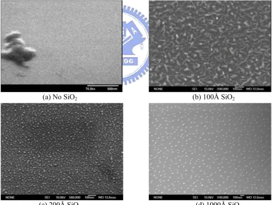
From the introduction, we know Lee et al. [2.6] have employed the Ni nanodot mask with diameter and density of about 41 nm and 5.3×109 cm-2, to form Si nanorods, but the disadvantage was that the self-aggregation of the Ni nanodots from Ni film coated on Si substrate usually takes up to 10 min even by rapid thermal annealing (RTA) process at 700oC in N2 ambient [2.6]. In order to improve the self-assembling process, we propose the quick formation of Ni nanodots on Si substrate covered with a thin buffered SiO2 layer. Figure 2.1 is the SEM image of the Ni nanodots self-aggregated on the SiO2 covered Si substrate with different SiO2 layer thickness under RTA at 850oC for 120 sec. As expected, Fig. 2.1(a) confirms that the Ni nanodots are unable to self-aggregate on pure Si wafer during such a short-term RTA process. On the contrary, we observe the apparent self-assembly of Ni nanodots on all of the SiO2 covered Si substrates. With a SiO2 thickness of 100 Å, the Ni layer initiates its self-aggregation to form a long strip, as shown in Fig. 2.1(b). However, the heat accumulation on such a thin SiO2 layer during RTA is still insufficient to complete the reshaping of Ni nanodots. By increasing the thickness of SiO2 layer from 100 Å to 200 Å, a coherent aggregation of Ni nanodots with almost half-sphere morphology can be seen in Fig. 2.1(c). Besides, the average diameter and the dnsity of the Ni nanodots are around 30 nm and 1011 cm-2 with the 200Å SiO2 under the Ni layer. If the thickness of the SiO2 layer enlarges to 1000 Å in Fig. 2.1(d), the size of Ni nanodots becomes larger about 40 nm than those obtained on thinner SiO2 film covered Si substrate in Fig. 2.1(c), whereas the Ni nanodot density greatly reduces to 1010 cm-2. It is thus concluded from the aforementioned results that the self-aggregation of Ni nanodots can be completed as the thickness of SiO2 increases to >200 Å, which is mainly attributed to the enhanced
heat accumulation effect happened in the thicker SiO2 layer during RTA. Apparently, the self-aggregation of Ni on SiO2 covered Si substrate is better than that on pure Si substrate due to their distinguishable difference in thermal conductivity (Si of 148 W/m-K and SiO2 of 1.35 W/m-K) [2.13]. Therefore, the SiO2 buffered layer can efficiently terminate the thermal dissipating from Ni layer to Si substrate such that the self-assembly of Ni nanodots can finished at a shorter annealing period. Therefore, the insufficient heat accumulation and strong adhesive problems happened at the Ni/Si interface can be solved by depositing a thin layer of SiO2 on Si substrate prior to the Ni evaporation and RTA processes. Comparing to the precious Korean results [2.6], we successfully increased the Ni dot density and shorten the annealing time.
(a) No SiO2 (b) 100Å SiO2
(c) 200Å SiO2 (d) 1000Å SiO2
Fig. 2.1Self-aggregation of Ni nanodots on Si substrates without or with SiO2 buffered layer of
different thickness.
2.3 RTA Temperature and time
The thin Ni film evaporated on the SiO2 film can easily to be conglomerated, resulting in the formation of Ni nanodot array on SiO2 substrate. Whether we change the annealing temperature or annealing time, both the thermal energy of annealing can be adjusted. From our experimental results, 850oC is the proper temperature for RTA annealing. As if the annealing temperature is too high, the Ni and Si atoms could obtain sufficient power to compose the SiNi2 compounds [2.12]. However, if the annealing temperature is too low, it spends more annealing time to congregate Ni film into randomized two-dimensional nanodot array. In the following experiments, we choose to fix the annealing temperature and vary the annealing time during RTA process.
(a) 30(s) (b)120(s)
(c) The diameter distribution of Ni nanodots
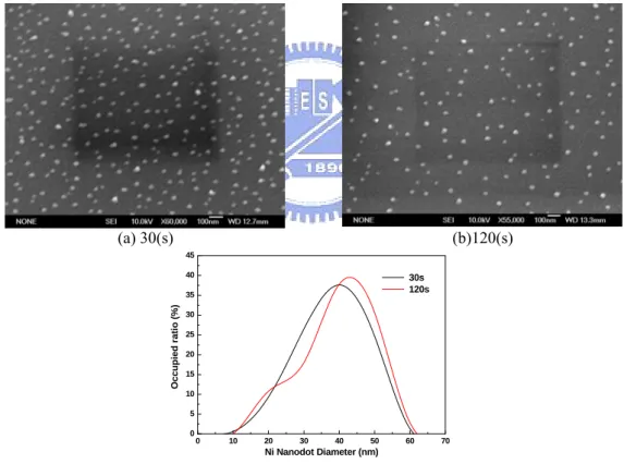
Fig. 2.2 SEM images of Ni nanodots after annealing for 30s and 120s at 850℃ shown in 2.2(a) and 2.2(b). Apparently the density of dots for shorterer annealing time is denser by comparing the plots in 2.2(c).
As shown in Fig. 2.2, we compare the variation in size and density of Ni dots assembling on 1000Å SiO2 layer under two different annealing periods. The average
0 10 20 30 40 50 60 70 0 5 10 15 20 25 30 35 40 45 Occu p ied r ati o (% ) Ni Nanodot Diameter (nm) 30s 120s
size and density of Ni nanodots annealing at 850oC for 30 sec are 37 nm and 1×1010 cm-2, respectively. Nonetheless, the average size and density of Ni nanodots annealing at 120 sec significantly increase to 40 nm and 7×109 cm-2. Fig.2.2(c) showed the peak Ni nanodots diameter shifted from 40 nm to 45 nm when the annealing time increased from 30 sec to 120 sec. This again confirms the trend of enlarging size and decreasing density under long annealing time. The Ni atoms can get more thermal energy to complete their precipitation process under longer annealing time. However, after rapid thermal annealing at 850oC between 20 and 26 sec, the Ni dots were formed on the 200Å SiO2 film shown in Fig.2.3.
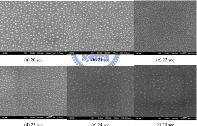
(a) 20 sec (b) 21 sec (c) 22 sec
(d) 23 sec (e) 24 sec (f) 25 sec
Fig. 2.3 The size and density of Ni dots as a function of the annealing time when the thickness of SiO2
is 200Å. The 22 sec annealing time at 850℃ is the optimum item for the densest density and the smallest diameter.
The shape of Ni nanodots becomes hemisphere-like with an average diameter varying from 33 nm to 75 nm, respectively. A largest density of 7.2×1010 cm-2 for the Ni nanodot with smallest size of 33 nm can be obtained after annealing at 850℃ for 22 sec. Figure 4 interprets the variation SEM image of Ni nanodot self-assembled at gradually lengthened annealing durations. The Ni film initially breaks into large strips
and slowly approaches a hemispheric shape with increasing RTA time, eventually these small Ni nanodots would congregate to larger nanodots if the annealing time prolongs to >30 sec. At annealing time between 22 and 26 sec, there is also a similar tendency on the size and density of Ni nanodots as compared to those shown in Fig. 2.3.
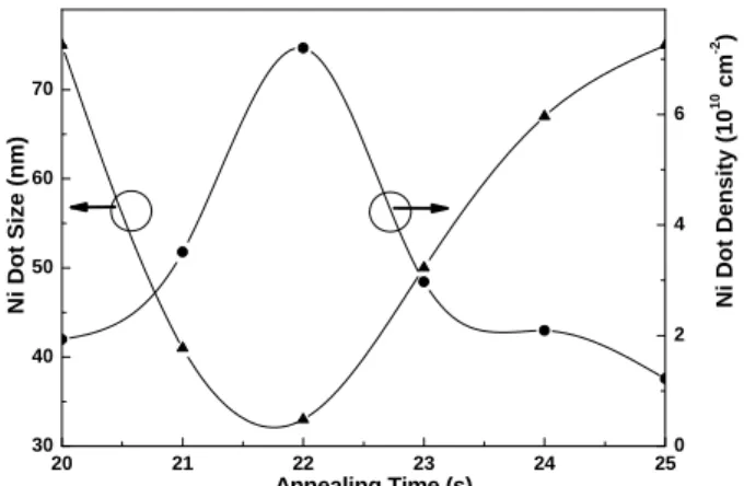
20 21 22 23 24 25 30 40 50 60 70 0 2 4 6 Ni Dot Size (n m) Annealing Time (s) Ni Dot Density (10 10 cm -2 )
Fig. 2.4 The size and density of self-aggregated Ni nanodot as a function of RTA annealing time.
In more detail, the size and distribution of the Ni nano-dots on the SiO2 film are mainly determined by thin oxide film thickness, RTA temperature, RTA time and Ni thickness. From the diagram of curves of Fig. 2.4, the optimum time is 22 seconds. The optimum annealing condition for Ni nanodot formation with highest density and smallest size are therefore set as 850oC for 22 seconds in our RTA annealing process. Such a sample has also been chosen as the Ni nano-mask for etching Si-nano-pillars. In addition, we also observe that the diameter of Ni nanodots becomes smaller with a decrease in the thickness of the deposited Ni layer [2.14].
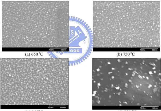
Following the annealing time, the annealing temperature is also a key point to aggregate Ni dots. A suitable annealing temperature can save annealing time and make the self-assembled Ni nanodots small and dense enough at the same time. In order to prove our intuition, we fixed the annealing time at 120 seconds、the thickness of Ni layer at 50Å、the thickness of SiO2 at 200Å and studied the effect of annealing temperature for Ni self-assembling. Then, the SEM images in Fig. 2.5 show the result that the Ni would gather to larger dots after the higher temperature annealing. However,
the density of Ni dots would decrease with the higher annealing temperature. So, too high annealing temperature such as 950℃ would be hard to control the dense and small Ni dots. On the contrary, the small-sized and dense Ni dots could be obtained after the lower temperature annealing but the annealing time needs to increase for completing the Ni self-assembling. As known from our experiment, it would take 100 seconds、60 seconds and 20 seconds at least to self-assemble Ni separately at the annealing temperature 650℃、750℃ and 850℃. The most appropriate annealing temperature is 850℃because Ni can self-assemble into the small size and high density the most quickly.
(a) 650 oC (b) 750 oC
(c) 850oC (d) 950 oC
Fig. 2.5SEM images of Ni dots after different annealing temperature for 120 s. Apparently the density of dots at lower annealing temperature is denser.
In more detail, the size and distribution of the Ni nano-dots on the SiO2 film are mainly determined by thin oxide film thickness, RTA temperature, RTA time and Ni thickness. From the diagram of curves of Fig. 2.4, the optimum time is 22 seconds. The optimum annealing condition for Ni nanodot formation with highest density and smallest size are therefore set as 850oC for 22 sec in our RTA annealing process.
Such a sample has also been chosen as the Ni nano-mask for etching Si-nano-pillars. In addition, we also observe that the diameter of Ni nanodots becomes smaller with a decrease in the thickness of the deposited Ni layer [2.14].
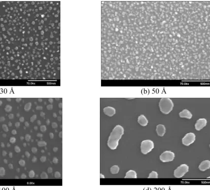
2.4 Ni thickness
Besides the factors of the SiO2 thickness 、annealing time and annealing temperature, we also observed that the diameter of Ni nanodots varied in the different thickness of the deposited Ni layer [2.7]. After analyzing the SEM images in Fig. 2.6, there is an apparent trend about the size and the density of Ni dots. When the Ni deposition is thicker under the same annealing conditions, the Ni would aggregate into larger dots and the dot number would decrease. Otherwise, the diameter of Ni dots exist a slight linear relation with the deposited Ni thickness. The approximately average diameters of Ni dots in Fig. 2.6(a) 、 (b) 、 (c) 、 (d) separately are 60nm、50nm、100nm and 200nm. Between the Fig 2.6(a) and Fig 2.6(b), the average diameters of Ni dots are nearly the same but the Ni dot number in Fig 2.6(a) is enormously smaller than in Fig 2.6 (b). This phenomenon is possibly caused by the uniformity of Ni deposition by e-beam evaporation. The depositing uniformity will be hard to control if the thickness of the deposited layer is small and close to the deposition rate. In addition, the information given by the SEM image in Fig 2.6 is that the shape of Ni dots will approach to circle if the thickness of Ni deposition is thinner. This is because the Ni self-assembling is more complete. The thicker the Ni deposition, the more time it will take to finish the Ni self-assembling. Eventually, the conclusion is that the optimum Ni thickness is 50Å to form the densest and smallest Ni nanodots as the etching mask.
(a) 30 Å (b) 50 Å
(c) 100 Å (d) 200 Å
Fig. 2.6SEM images of Ni dots formed from different thick Ni layer at 850 oC for 120 s. Apparently
the density of dots with the thinner deposition of Ni layer is denser.
2.5 Conclusion
In conclusion, we successfully demonstrate a rapid self-assembly method for aggregating Ni nanodots on Si substrate by using a highly heat-accumulated and less-adhesive SiO2 buffered layer. The Ni nanodot is relatively difficult to be self-aggregated on the Si substrate without SiO2 buffered layer due to the highly heat dissipated feature of Si substrate with a thermal conductivity of 148 W/m-K. The 200Å thin SiO2 layer prevents the formation of NiSi2 compounds and facilitates the self-assembly of Ni nanodots from retaining the thermal power on the SiO2 layer due to its ultralow thermal conductivity of only 1.35 W/m-K. The required annealing time for synthesizing the Ni nanodots with comparable density and size is greatly shortened to <30 seconds. The self-aggregated Ni nanodots with highest density and smallest size of 7.2×1010 cm-2 and 33 nm, respectively, are obtained at the optimized RTA condition at 850oC for 22 sec. The larger size and smaller density of Ni nanodots will be obtained after RTA if the SiO2 film or the Ni layer becomes thicker. Raising the RTA
temperature 、lengthening the RTA time and depositing thick SiO2 film or Ni layer will concurrently cause the effects of size enlargement and density dilution.
2.6 Reference
[2.1] A. G. Nassiopoulos, S. Grigoropoulos, E. Gogolides, and D. Papadimitriou, Appl. Phys. Lett. 66, 1114 (1995)
[2.2] P. B. Fischer, K. Dai, E. Chen, and S. Y. Chou, J. Vac. Sci. Technol. B 11, 2524 (1993)
[2.3] H. I. Liu, D. K. Biegelsen, N. M. Johnson, F. A. Ponce, and R. F. W. Pease, J. Vac. Sci. Technol. B 11, 2523 (1993)
[2.4] Y. Homma, P. Finnie, T. Ogino, H. Noda, and T. Urisu, J. Appl. Phys. 86, 3083 (1999).
[2.5] D. Crouse, A. Y.-H. Lo, E. Millar, and M. Crouse, Appl. Phys. Lett. 76, 49
(2000).
[2.6] J. S. Lee, S. K. Kim, G. Y. Yeom, J. B. Yoo, and C. Y. Park, Thin Solid Films
475, 41 (2005).
[2.7] H. W. Huang, C. C. Kao, T. H. Hsueh, C. C. Yu, C. F. Lin, J. T. Chu, H. C.
Kuo, and S. C. Wang, Mat. Science & Eng. B 113, 125 (2004).
[2.8] K. M. Klein, Z. Jiantao, A. Gewirtz, D.S. Sarma, S. Rajalakshmi, S. K. Sitaraman, 2005 Proceedings. 55th Electronic Components and Technology (IEEE Cat. No. 05CH37635). IEEE. 1, 538-71 (2005)
[2.9] J. Narayan and S. Oktyabrysky, J. Appl. Phys. 92, 7122 (2002) [2.10] J. Narayan and B. C. Larson, J. Appl. Phys. 93, 278 (2003).
[2.11] D. Aurongzeb, S. Patibandla, M. Holtz and H. Temkin, Appl. Phys. Lett. 86, 103107 (2005)
[2.12] H. Zhou, D. Kumar, A. Kvit, A. Tiwari, and J. Narayan, J. Appl. Phys. 94, 4841 (2003).
[2.13] J. Zhao, J. Sullivan, J. Zayac, and T. D. Bennett, J. Appl. Phys. 95, 5475 (2004).
CHAPTER 3
Formation of Si Nanopillars
3.1 Introduction
Because of the using variety, Si one dimensional structures were extensively researched in the fabrication and analysis.[3.1-3.3] There are two major ways to form the Si one dimensional structure which are the thermal growth with the catalysis Au or Fe [3.4-3.5] and the dry etching by reactive ion etching [3.6-3.8]. The disadvantages of the thermal growth are the unable control for the diameter and the growing direction comparing to the dry etching. The reactive ion etching and electrochemical etching were employed as two etching procedures to obtain Si nano-pillar array. Traditional approaches for fabricating sub-micron or nano- Si structures, such as the Si nano-pillars, mainly rely on the electron-beam (E-beam) lithography [3.9], which provides accurate size and shape control. The production of <10-nm nano-pillar array under the assistance of E-beam lithography has been reported by Toshihiko and Papadimitriou. However, it is impractical to employ the E-beam lithography for large-scale fabrication due to its high cost and low writing speed. Nowadays, noble metal (Au or Ag) based nano-dot arrays have been extensively used as nano-masks to replace the E-beam lithography. Recently, Ni has been considered as an alternative to the noble metals. The Ni nano-dot mask is not only easy to control its size but also cheap in its formation process as compared to that of the e-beam lithography. In ref. 3.3, using the Ni nanodots as an etching mask, the Si nanopillars were performed by ICP-RIE with the etching gases carbon tetrafluoride (CF4) and sulfur hexafluoride (SF6). The diameter and height of the formed Si nanopillars are about 41 nm and 472 nm with the aspect ratio higher than 10. Nevertheless, their results can be improved that the density is too sparse to enhance the luminescence, and the self-aggregation of the Ni nano-dot from a
Ni film coated on a Si substrate usually takes up to 10 min even by a rapid thermal annealing (RTA) process at 700oC in the N2 ambient. With the novel approach, the formation of the Si nano-pillar array can be mostly realized by the reactive ion etching of oxide-covered Si substrate edcapped with the mask of self-assembled Ni nanodots. A Si nano-pillar array has been shown to have the potential for many applications such as being photonic crystals [3.10], data storage [3.11], field electron emitter [3.12], nanoscale transistors [3.13-3.14] and light emitting devices [3.15]. Otherwise, the light emitting efficiency could also be enhanced with the aid of the quantum confined Si nano-pillars.
3.2 Experimental Process
In previous experiment, it is hard to achieve the aggregation of evaporated Ni film on pure Si wafer. This is because the adhesion between Ni and Si is too good to be make Ni self-assembled. Such a problem can be solved by depositing a thin layer of SiO2 between Ni and Si. In our case, a buffered layer of 200Å-thick SiO2 is deposited by plasma enhanced chemical vapor deposition (PECVD) under standard recipe. Afterwards, a 50nm-thick Ni film is evaporated on the SiO2/Si substrate using an E-beam evaporating system with Ni deposition rate of 0.1 Å/s at an applied current of 70 mA. Subsequently, the rapid thermal annealing (RTA) process at 850oC for 22 seconds under the N2 flowing gas of 5 sccm is performed to format randomized Ni nanodot pattern on SiO2/Si substrate. The average diameter and density of Ni nanodots are 33nm and 7.2×1012 cm-2. By using the Ni nano-dot pattern as an etching mask, the Si substrate is dry-etched in a planar type ICP-RIE system (SAMCO ICP-RIE 101iPH) at RF frequency of 13.56 MHz. The ICP has a reactive chamber connected to a load-lock chamber, wherein the etching gas mixture of CF4 and Ar gases were introduced into the reactive chamber through individual electronic mass flow
controllers (MFCs). The flowing rate of each gas is adjusted within an accuracy of about a standard cubic centimeter min (sccm). An automatic pressure controller is placed near the exhaust end of the chamber to control the chamber pressure. The gas mixture condition of CF4/Ar = 40/40 sccm with the ICP/Bias powers set at 100W/50W and chamber pressure of 0.66 Pa during an etching duration of 5~7 minutes. If the etching parameters such as source power, bias power, and pressure and gas composition are investigated and optimized, Si nano-pillar arrays with tunable diameters of smaller than 100 nm can be formed. The fabricating process is shown in Fig. 3.1. After etching by ICP-RIE, the SiO2 and Ni on the Si nanopillars would be removed by dipping in the HF solution and HNO3 solution. Then, the pure Si nanopillar sample must be stored in the methyl alcohol to avoid the oxidation day by day. For analyzing the morphology of Ni nano-dot, the dimension and density of the Si nano-pillar array were estimated by the scanning electron microscope (SEM, Hitachi FE-SEM S-5000) and the standard atomic force microscopy (AFM).
Fig. 3.1 Schematic illustration of Si nano-pillar arrays using Ni/SiO2 as nano-masks formation. The
reaction products after RTA and ICP-RIE etching, leading to the formation of Si nano-pillar arrays.
3.3 Results & Discussions
3.3-1 Gas flowing
The choices of gases for etching are very weighty because the etching rate and selectivity are extremely distinct by using the different etching gases. [3.15] In the
p-Si sub SiO2 200Å Ni 50Å Si- sub SiO2 RTA ICP Si-sub
magnitude and ratio of the nixing gases are also the key point to get high etching rate and selectivity. SF6、CF4、CHF3、Ar、O2 and N2 are the gases mainly to etch Si and SiO2. [3.6-3.8] SF6、CF4 and CHF3 are the major etching sources and the etching rate can be enhanced by addition of Ar、O2 and N2. As for etchant gas, we chose the O2, CF4 and Ar at the beginning of experiment. CF4 is the main gas for etching SiO2 and Si. Ar is also main gas able to increase the vertical-etching potential. In our opinion, O2 is the mirror gas which should speed up the etching rate. Nevertheless, the aid of O2 isn’t apparent and the oxygen plasma causes a lot of defects such weak oxygen bond and the neutral oxygen vacancy in the Si nano-pillars analyzed from the photoluminescence. On account of the above reason, we have not used O2 as etchant gas.
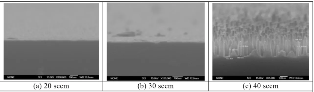
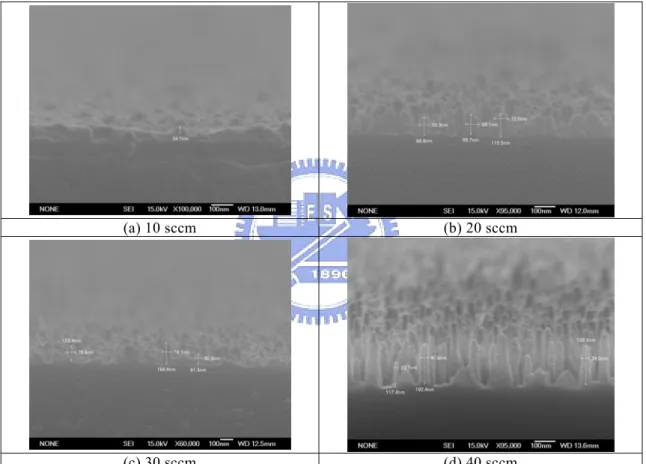
In our all etching process, the gaseous mixture of CF4 and Ar were adopted. If the etching pressure、rf power、bias power、 etching time and Ar flowing are fixed at 0.66 pa、100 W、50 W、7 minutes and 40 sccm (standard cubic centimeter), we can clearly observe that the optimum etching depth of Si nanopillars occurred at the CF4 flowing 40sccm from Fig. 3.2. The average diameter and length of the Si nanopillars are 35 nm and 170nm and the aspect ratio is nearly 5.
(a) 20 sccm (b) 30 sccm (c) 40 sccm
Fig 3.2 The SEM images of Si nanopillars formed under three different flowing of etching gas CF4.
various Ar flowing from 10sccm to 40sccm. From Fig. 3.2, we can find that the etching depth of Si nanopillars would be shallow if the Ar flowing were too small. So we can get the optimum depth of Si nanopillars happened with the Ar flowing 40 sccm in our experiment because the etching rate can be enhanced by addition of Ar. The average diameter and length of the Si nanopillars are 35 nm and 170nm and the aspect ratio is nearly 5.
(a) 10 sccm (b) 20 sccm
(c) 30 sccm (d) 40 sccm
Fig 3.3 The SEM images of Si nanopillars formed under four different flowing of etching gas Ar.
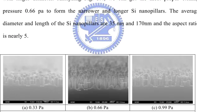
3.3-2 Chamber Pressure
One of the major factors affecting the etching results is the etching pressure during the etching process. If the pressure is too high, the etching rate will becomes too fast. If the etching rate is too high, the selectivity between the mask and the Si
will decline and the side etching will also be serious to cut the Si nanopillars. So, the Si nanopillar won’t be formed under the high etching pressure. As our experience, the etching pressure can’t be more than 1.5 pa. On the contrary, the etching rate is too slow to etch Si in a few periods under the high etching pressure. In a conclusion, the appropriate etching pressure is very significant during the etching process. As shown in Fig. 3.4, we can observe that the etching depth is proportion to the etching pressure but not linearly. But the diameter of the Si nanopliars is the smallest at the 0.66 pa pressure. This is mainly resulted from the side etching. The diameter of the Si nanopillars would be decreased by the highly side effect, but too high side effect would cut the Si nanopillars with the small diameter and leave the Si nanopillars with larger diameter. Analyzing Fig. 3.4, we can get the most proper etching pressure 0.66 pa to form the narrower and longer Si nanopillars. The average diameter and length of the Si nanopillars are 35 nm and 170nm and the aspect ratio is nearly 5.
(a) 0.33 Pa (b) 0.66 Pa (c) 0.99 Pa
Fig. 3.4 The SEM images of Si nanopillar formed at three different etching pressures.
3.3-3 Etching Power
To perform the Si nanopillar formation, the key issue is the proper magnitude of the etching power. There are two kinds of powers included in the ICP-RIE equipment that are the rf and bias power. The rf power decides the isolating level of the etching gases
and the dc bias power controls the vertical level of the side wall. In this experimental process, the experimental tests for the two powers are the ratio and magnitude. From the 45° view angle of the SEM images in Fig. 3.5, we can compare the different formation of Si nanopillars at the instinct power ratio. In this comparison, we chose the optimum results which are the largest length. So, the etching time is also different for the different power ratio. The etching time is 3 min、5min and 50 s when the rf/bias power is 300(W)/100(W)、200(W)/100(W) and 200 (W)/200(W).
(a) 300(W)/100(W) (b) 200(W)/100(W) (c) 200(W)/200(W)
Fig. 3.5 (a) shows the apparently triangle shape of Si nano-pillar. (b) The sharper sidewall of Si nanopillar. (c) A sharp side-wall of Si pillar with insufficient height.
Figure 3.5(a) shows that the by-product appears and the shape of Si nano-pillar resembles a pyramid when the ratio is 3. Then the density is the smallest and the diameter is the largest. The cause is isotropic etching erodes the smaller pillar, and the reason for a pyramid shape is that the vertical etching-rate is not bigger than the side etching-rate so the diameter of the pillar becomes bigger after longer etching time. Finally, the etching rate is dominated by the power. So we are sure the ratio of 3 is too big to get a straight pillar. Figure 3.5(b) shows the success of the formation of Si nanopillars with a perpendicular sidewall at the ratio of 2. The density and diameter of Si nanopillars are 2.8×1010 cm-2 and 29 nm. Figure 3.5(c) shows the straight but short Si nanopillars at the ratio of 1. This is because the vertical etching is too big to balance the etching selection between Ni and Si, we can see the Ni mask disappeared during the etching.
0 1 2 3 4 4 8 12 16 20 24 28
Power Ratio (ICP power / Bias power)
D e nsit y (*10 9 cm -2 ) 30 40 50 60 A verage diamet er (n m)
Fig. 3.6 Different ratio of ICP power over bias power has different influence on the vertical level of Si pillars’ side-wall.
In another word, the appropriate ratio of bias and ICP power is the key point to get sharp sidewall and large height of Si nanopillars. After analyzing the SEM data in Fig. 3.6, we can know the ratio of bias power over ICP power had great influence on the character of Si nano-pillars such as the diameter and the density. In summary, we know that the ratio of 2 is the most suitable for the formation of Si nanopillars. From Fig. 3.7 we can know if the magnitude is bigger, the Si nano-pillars will be longer and the size of them will be wider. The average size of bias/ICP power at 100(W)/200(W) is 29 nm and the average one at 50(W)/100(W) is 44nm. The average height of 100(W)/200(W) is 150nm and the one of 50(W)/100(W) is 250nm. From the cross-session image in Fig. 3.7, Si nanopillars with high aspect-ratio were formed at the bias/ICP power of 2 whatever the magnitude of the powers is.
(a) 100(W)/200(W) (b) 50(W)/100(W) Fig. 3.7 The different magnitude of power with the same ratio of bias and ICP power.
After testing the generally proper rf / bias power ratio and magnitude, the individual effect of the rf and bias powers were also studied. In this part, the etching mask is the Ni nanodots forming after the RTA at 850℃ for120 s and the density of Ni nanodots is about 5x1011 cm-2. Analyzing from Fig 3.8, it is clearly that the magnitude of rf power affects the etching rate and selectivity a lot. Nevertheless, the etching rate is tradeoff with the etching selectivity. In Fig. 3.8 (a), the etching selectivity is high but the etching rate is very low when the rf power is 50 W. The average depth is about 100nm. In Fig.3.8 (b), the etching selectivity and rate are good and the average depth is 170 nm when the rf power is 100 W. In Fig. 3.8 (c), the etching selectivity and rate are the optimum tradeoff for the largest depth of 400nm when the rf power is 150 W. In Fig. 3.8(d), the Si nanopillars disappeared for the low etching selectivity and high etching rate. So, the rf power of 150 W is the most appropriate for balancing the etching selectivity and rate. The average diameter and length of the Si nanopillars are about 50 nm and 400 nm, so the aspect ratio is about 8.
(a) 50 W (b) 100 W
150 (W) 200 (W)
Fig. 3.8 The cross section SEM images of the Si nanopillars were formed at the different RF power from 50 W to 200 W
For the dry etching by ICP-RIE, the vertical etching is controlled by the bias power. And it affects the etching rate and selectivity more sensitively than rf power. After observing the SEM images in Fig. 3.9, the Si nanaopillars were almost formed at the bias power of 50 W. In Fig. 3.9 (a), the etching depth is nearly 0 nm at the bias power 0 W. From Fig. 3.9(a)-(c), the etching depth is proportion to the magnitude of the rf power. But, the Si nanopillars were etched over on the account of too huge power in Fig. 3.9 (d). Finally, we get the most suitable magnitude of bias power is 50 W. The average diameter and length of the Si nanopillars are 35 nm and 170nm and the aspect ratio is nearly 5.
(a) 0 W (b) 25 W
(c) 50 (W) (d) 75 W
Fig. 3.9 The cross section SEM images of the Si nanopillars were formed at the different bias power from 0 W to 75 W.
3.3-4 Etching Time
By the intuition, the etching depth will be longer if the process takes more time to
etch. From Fig. 3.10 (a)-(c) the etching result matches the intuition. However, the etching time extending over the optimum time would over etch the Si nanopillars. Because the Ni mask also etched by plasma, the long-timed etch would remove the Ni completely. The Si nanopillars without Ni cap would shorten during the etching process. In our etching process, the optimum etching time is 7 min when the pressure 、CF4/Ar flowing and rf/bias power are 0.66 pa、40(sccm)/40(sccm) and 100(W)/50(W). The average diameter and length of the Si nanopillars are 35 nm and 170nm and the aspect ratio is nearly 5.
(a) 3mins (b) 5mins
(c) 7mins (d) 9mins
Fig. 3.10 The cross section SEM images of Si nanopillars were etched for different time from 3 min to 9 min
3.4 Conclusion
Si nanopillars with high aspect ratio were formed on Si substrate with the self-assembled Ni nanodots by ICP-RIE. The etching depth was proportion to the magnitude of CF4 flowing、Ar flowing、the chamber pressure、the etching time、 the bias power and the rf power, but the etching selectivity between the Si and Ni dots is completely opposite. Because of the tradeoff of the etching depth and the etching selectivity, there is an optimum value to every etching parameter. In our experiment, the optimum aspect ratio of Si nanopillars happened with the average diameter and depth of 50 nm and 400 nm in our experiment when the gas flowing of CF4 and Ar、the bias/rf power、the chamber pressure、the etching time were set at
40sccm、40sccm、50(W)/150(W)、0.66pa and 7 min. Comparing to the results of the Korean [3.7], the density of the Si nanopillars in our experiment is over ten times larger than the Korean because of the Ni nandot mask of the high density. Limited to the size of the Ni nanodots, the average diameter of the Si nanopillars is in the range of 30 nm to 50 nm.
3.5 Reference
[3.1] D. Papadimitrioum and A. G. Nassiopoulou, J. Appl. Phys. 84, 1059 (1998)
[3.2] T. V. Torchynska, J. A. Hernandez, A. I. D. Cano, F. G. B. Espinoza, Y. Goldstein, A. Many, J. Jedrzejewskii, L. Y. Khomenkova, B. M. Bulakh and L.V. Scherbina, Phys. Stat. Sol. 2, 382 (2003)
[3.3] D. D. D. Ma, S. T. Lee and J. Shinar, Appl. Phys. Lett. 87, 033107-1 (2005)
[3.4] Y. Homma, P. Finnie, T. Ogino, H. Noda and T. Nrisu, J. Appl. Phys. 86, 3083 (1999)
[3.5] Y. L. Chueh, L. J. Chou, S. L. Cheng, J. H. He, W. W. Wu and L. J. Chen, Appl. Phys. Lett. 86, 133112 (2005)
[3.6] C. W. Kuo, J. Y. Shiu and P. Chen, Chem. Mater. 15, 2917 (2003) [3.7] M. J. Kim, J. S. Lee, S. K. Kim, G. Y. Yeom, J. B. Yoo and C. Y. Park,
Thin Solid Films 475, 41 (2005)
[3.8] T. Tada and T. Kanayama, J. Vac. Sci. Technol. B 16, 3934 (1998)
[3.9] V. Poborchii, T. Tada, and T. Kanayama, Opt. Commun. 210, 285 (2002). [3.10] K. Sunouchi, H. Tkato, N. Okabe, T. Yamada,T. Ozaki, S. Inoue, K.
Tech. Dig. 23 (1989).
[3.11] A. V. Karabutov, V. D. Frolov, A. V. Smakin, and G. A. Shafeev, IEEE Proceedings of the 14th International Vacuum Microelectronics Conference (IVMC2001) 115 (2001).
[3.12] M. Terauchi, N. Shigyo, A. Nitayama, and F. Horiguchi, IEEE Trans. Electron. Dev. 44, 2303, (1997).
[3.13] F. D. Bauer, Solid-State Electron. 48, 705 (2004).
[3.14] A. G. Nassiopoulos, S. Grigoropoulos, and D. Papadimitriou , Appl. Phys. Lett. 69, 2267 (1996).
[3.15] W. Beyer, M. Lejeune, J. Muller, U. Zastrow, M. Albert, T. Robler, Proceedings of 3rd World Conference on Photovoltaic Energy Conversion (IEEE Cat. No.03CH37497) 2, 1584 (2003)
Chapter 4
Optical and Electrical Characteristics of Si
nanopillars
4.1 Introduction
The increasing interest in low dimensional Si structures for potential applications in optoelectronics has given rise to significant progress on the development of both the fabrication process and the related physical mechanisms for versatile Si nanostructures. [4.1-4.5] Theoretical studies of Si quantum wires confirm that there is a transition of the band structure from indirect to direct bandgap in Si nanostructures due to the electron confinement in nanostructures, [4.6-4.8] which may be corroborated by characterizing the luminescent spectroscopy of the well controlled and ordered nanostructures. The intriguing electrical, optical, mechanical, and chemical properties, suggest that Si quantum wires may be used for developing field emitting devices [4.9]、surrounding gate transistors [4.10]、2-D photonic crystal slab [4.11] and bio-sensors, [4.12] etc.
In 1998, Papadimitriou et al. fabricated highly anisotropic Si nanopillar array with an aspect ratio of 25:1 and a diameter <100 nm by using nano-lithography and dry-etching after several cycles of thermal oxidation and oxide removal procedure.[4.13] The anisotropic Si nanopillar array emits photoluminescence (PL) at wavelength of 500-600nm, while the PL efficiency and wavelength were found to be corrected with the wavelength and the polarization state of the pumping laser. Such a dependence was attributed to the quantum-confined polarization effects In 2004, Yanagiya et al. tired to grow Si nanowires on sapphire with a diameter of 50 nm and a height of 1 nm by using a disilane (Si2H6) gas-source based molecular beam epitaxy (MBE). [4.14]. Visible
low- and room-temperature PL from the Si quantum wires was observed at central wavelength of 750 nm. The PL intensity at 9 K is blue-shifted and is 20 times larger than that at 300 K. On the other hand, Nassiopoulos et al. have implemented the electroluminescent (EL) device based on Si nanopillars in 1996. [4.15] Visible light emission was observed under a forward bias the voltage exceeding of 12–14 V. The EL characteristics were similar to the PL, which is attributed to a high electric field electronic transporting through the Si nanowires.
In this chapter, we discuss the power dependent PL of the original and oxidized Si nanopillar array. The surface reflection of Si nanopillar array on Si substrate are analyzed and compared with that of the bulk Si wafer. Furthermore, the current-voltage and capacitance-voltage characteristics of Si nanopillar array are also studied.
4.2.1 Experimental
The measuring setup is shown in the Fig. 4.1. A HeCd laser at 325 nm employed as the pumping source, and a Triax 320 spectrometer, with a photomultiplextor tube (PMT) are employed to analyze the PL of Si nanopillars. The spot size and pumping power of the laser are set as 100 μm and 25 mW, respectively. A notch filter is installed to reject the scattered pumping laser from sample surface. To avoid the gradual oxidation effect, the Si nanopillar sample is dipped in methyl alcohol before diagnosis. The sample is dried in the air for 2 minutes prior to the measurement.
Fig. 4.1 The PL measurement is set up with the 325nm He-Cd laser、a pair of mirrors and focal Lenses、 a beam splitter、a Triax320 spectrometer、photonic multiplying tube.
To pump the Si nanopillar array at higher intensity, a confocal microscope based micro-photoluminescence (μ-PL) system is introduced. The sample is placed on a 2-D stage that can be scanned by a piezoelectric feedback controller with a position accuracy of less than 3 nm. A 3-D stepping motor controlled stage was used to align the microscopes collinearly. A 15x UV objective lens with a numerical aperture 0.32 is used to collect the PL from the sample into a monochromator-PMT link through an optical fiber with core diameter of 25 μm and 600 nm, respectively. A high-resolution digital camera is used to record the microscopic images of the sample. The optical resolution of the confocal microscope is about 1 μm and determined by the core-diameter of the optical fiber. The pumping power of 25 mW corresponds to an intensity of 31800 W/mm2 under a strongly focused condition.
Sample Jobin-Yvon Triax 320 Spectrometer 3 32255 nnmmHHee--CCddLLaasseerr Mirror 1 Mirror 3 P PMMTT
Focal lens 1 Focal lens 2 Mirror 2 Stage 360nm High Pass Filter Power density: 300 W/cm2 Range
Fig. 4.4 The experimental setup contains the confocal microscopy and micro-photoluminescence (μ-PL) system that can focus the laser beam to 1μm.
4.2.2 Structural Damage Dependent PL
After removing the mask made by Ni nanodots and SiO2 film on Si substrate, the height and density of the Si nanopillars are measured as 30-100 nm and about 5.4×1010 cm-2 by using atomic force microscopy and scanning electric microscopy. The as-etched Si nanopillars exhibit strong PL at blue-green wavelength instead of near-infrared region due to the strong surface damage occurred during the ICP-RIE process with the etching gas O2. Such a visible PL has previously been attributed to the oxygen defects accompanied with the oxygen plasma destruction.
Height 68.8 Height 29.6
(a) (b)
Fig. 4.2 (a) SEM image of Si nano-pillars after removing the Ni and SiO2 layers at the etching-power
ratio of 2 for 3 min. (b) AFM data including 3-D 45°view angle image and the height profile.
3 5 0 4 0 0 4 5 0 5 0 0 5 5 0 6 0 0 0 2 0 0 4 0 0 6 0 0 8 0 0 1 0 0 0 1 2 0 0 1 4 0 0 1 6 0 0 1 8 0 0 C e n t e r W i d t h H e i g h t -4 1 8 . 6 2 3 9 . -4 3 1 1 1 5 8 . 6 4 5 1 . 5 9 8 4 . 4 7 6 5 6 9 . 8 9 In t e n s it y ( c o u n t .) W a v e l e n g t h ( n m )
Fig. 4.3 Photoluminescence of Si nano-pillars in (a) and decomposed by two Gaussion fits at 418 and 451 nm.
Previously, the luminescent centers in the SiO2: Si+ corresponding to the visible PL was comprehensively investigated which the weak oxygen bond (WOB) and the neutral oxygen vacancy (NOV) defects at emitting wavelengths of around, 415 nm and 455 nm, respectively [4.16-4.19]. The Si nano-pillar sample presents a strong and broad PL spectrum between 400 and 450 nm. After decomposing with a multi-Gaussian function, two principle luminescent centers at 418 and 451 nm with corresponding linewidths of