A 0.8-8 GHz 9.7 mW Analog-Digital Dual-Loop Adaptive-Bandwidth DLL
Based Multi-Phase Clock Generator
Tsung-Te Liu and Chorng-Kuang Wang
Graduate Institute of Electronics Engineering, and Department of Electrical Engineering, National Taiwan University, 106 Taipei, Taiwan R. 0. C.
E-mail: [email protected], [email protected]
Abstract
This paper presents an implementation of a lowjitter wide-range multi-phase clock generator using a delay- lucked loop (DLL) for ultra-wideband (UWB) application.
The analog-digital dual-loup adaptive-bandwidth structure in conjunction with a complementary phase detector
(PD)
ensures low-jitter clock generation over a wide fi.equency range. The selffeedback technique reduces the power consumption of the level-shifter circuit 50% a1 least. The 0.18-pm CMOSprotatype ahibits the maximum cluckjitter of 3 . 9 ~ s (rms) and 2 8 . 7 ~ ~ (pk-pk) at an output clock rate of 1.6 tu 8 GHz (50-250 MHz inputreference frequency) and consumes 9.7 mWfrom a 1.8-V supply at 8 GHz.
1.
IntroductionOne critical aspect of VLSI implementation of pulse- based UWB radio is the accurate generation of timing signals to support reliable data communications [I]. Phase-locked loops (PLLs) and delay-locked loops (DLLs) have been typically employed to generate the required accurate high-frequency system clock from a low- frequency, precise, and stable oscillator. Usually, DLLs are easier than PLLs to implement the clock generator. A DLL is unconditionally stable and only needs one capacitor in its first-order loop filter. Moreover, a DLL offers better jitter performance than a PLL because phase errors induced by supply or substrate noises do not accumulate over many cycles in the delay line
[Z].
The adaptive-bandwidth architecture is often adopted in the design of the DLL to ensure optimum performance over a wide frequency range and across process, voltage, and temperature (PVT) variations [3], [4]. However, these conventional DLLs would lose the adaptive-handwidth characteristic and generate more jitters inherently if the DLL output signal swing which is proportional to loop control voltage approaches the device threshold [ 5 ] , [6]. Therefore, the conventional adaptive-bandwidth design still suffers from large performance variation when the DLL needs to operate across a wide frequency range.This paper describes an adaptive-handwidth DLL for the low-jitter wide-range multi-phase clock generation in UWB application. The proposed analog-digital dual-loop structure maintains the output signal swing at a sufficiently high voltage level to ensure jitter performance over a wide operating frequency range. The This work was supported in part by MediaTek hc. Hsin Chu, Taiwan 300.
complementary phase detector (PD) and self-feedhack level shifter are introduced to further improve the jitter performance and reduce the power consumption respectively.
2.
DLLArchitectureI
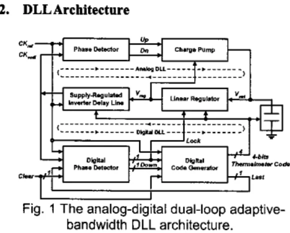
Fig. 1 T h e analog-digital dual-loop adaptive- bandwidth DLL architecture.
I
The proposed dual-loop DLL shown in Fig. 1 is
composed of a digital DLL and an analog DLL. The
digital DLL first judges delay relationship between the
input reference clock CK,<,and delayed clock from the last stage of delay line CKVcd, by digital phase detector which signals the following digital code generator to generate digital control word of 4-bits thermometer code. The delay of the delay line can he coarsely tuned by the digital control code word through sequentially turning off four additional parallel banks of delay line placed around the main delay line. The lock-in process within digital DLL would continue until the delay of the delay line has been placed in the optimum lock-in range of the analog DLL.
The analog DLL then takes over the loop and finely tunes the delay of the delay line to eliminate the remaining phase error. The linear PD, the charge pump (CP), the loop filter, the linear voltage regulator, and the supply regulated delay line comprising 16 pseudo-differential delay elements compose the analog DLL.
Fig. 2 shows the detailed timing diagram of the dual- loop DLL when the DLL starts from reset state. The four additional parallel banks of delay line are initially all turned on (corresponding to the code word 0000) and the delay of the delay line is set to its minimum delay in order to avoid harmonic-locking problem. The digital code generator then keeps updating the digital control code word to increase the delay of the delay line by sequentially turning off the parallel banks of the delay line. If the delay of the delay line is larger than one period of CKr4 the
digital phase detector would immediately respond by activating the Lock control signal and setting the digital
control code word to its prior value. The analog DLL takes control of the loop from this time with minimum phase error, which means that it can finally lock to the highest possible loop control voltage at steady state. This two-step lock-in process ensues the proposed DLL can keep good jitter performance while achieving a wide operating
frequency range. .. , :: 1 8 /i j : m . . .. , ,
-
, . ,, ., ,. . v.. c 1 M 1 U ~ ~ l o C u W+
-oYrsu-r-nn-
Fig. 2 Timing diagram of the dual-loop DLL. The loop bandwidth of the charge pump based DLL can be expressed as [3]:
(1) 1
w N = I , . KDL . FREF . -
CL
where
IC"
is the charge pump current, CL is the loop filter capacitor, KDL is the delay line gain, and FmTF is the frequency of the input reference clock. In the analog- digital dual-loop DLL architecture, because the delay of the delay line is controlled by both the number of the tumed-on delay line hanks and the regulated supply voltage, KDL is related to the value of the digital control code word D,,rf and loop control voltage V,, by:where K , is a proportional constant and V , is the threshold
voltage of the transistor. If the charge pump is biased with
VCel and the number of capacitors in the loop filter is determined by D,,,,, it can be shown:
I C H = K 2 . (VcrA - 7'
y
(3)
(4)
CL = K3 ' D,,d
where K2 and K3 are proportional constants. By combining (1)-(4), the loop bandwidth of the dual-loop DLL is then given by:
Equation ( 5 ) indicates w x
is
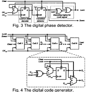
directly proportional to FREF, which means the dual-loop DLL has the adaptive- bandwidth characteristic similar to the conventional analog adaptive-bandwidth DLLs [ 3 ] , [4]. Therefore, the dual-loop DLL possesses all the advantages of the adaptive-bandwidth architecture no matter which digital control code word Dcni is chosen to acquire locking. 3. Circuit Design3.1. Digital Phase Detector and Code Generator Fig. 3 shows the schematic of the digital phase detector, which is composed of a lock-in state decoder, a
transition detector, and decoding logics for Lock signal. The present lock-in state can be determined by sampling
CK,, at the rising edge of as shown in Fig. 2. The Lust signal generated by the digital code generator is activated when the delay of the delay line has reached the maximum value (corresponding to the code word I I I I ) in the lock-in process of the digital DLL. Fig. 4 shows the schematic of the digital code generator, which consists of six code cells to produce 4-hit thermometer code. The additional two cells are used for pipelining in order to increase the timing margin allowed for circuits to response.
-
II I
... , ... .
Fig. 3 The digital phase detector.
Fig. 4
3.2. Complementary Phase Detector
Fig. 5 The complementary phase detector
4
(a) (b)
Fig.
6
(a)
Complementary PD and (b) conventional PD with CP.Fig. 5 shows the schematic of the complementary PD
circuits, which are based on one basic dynamic logic PD
cell and its complement. The complementary property is established by using the complementary input signals and interchanging the positions of the two dynamic logics. The additional inverters interposed between dynamic logics help the PD periodically to produce a chain of short pulses in the locked state which can reduce the dead zone of the PD effectively. The complc_mentary PD can directly generate two control signals Up and Dn with zero skew difference to sense the following CP circuit charging or discharging the loop filter, as shown in Fig. 6(a). The conventional approach shown in Fig. 6(h) uses Ln additional inverter and a transmission gate to produce Up and Dn control signals. However, the delays caused by the inverter and the transmission gate are usually hardly matched under PVT variations, which causes additional ripples on the loop control line and thus results in a deterministic jitter of the DLL output when the loop is locked.
3.3. Supply-Regulated Delay Line
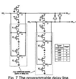
Fig. 7 The programmable delay line. The delay line shown in Fig. 7 is based on simple CMOS inverter stages with weak cross-coupled inverters to minimize skew. The CMOS inverter delay element has lower power consumption than the delay element based on source-coupled differential pair. The loop control voltage
V,, can adjust the delay by varying thc supply voltage of the delay line through linear regulator. Four additional parallel banks of delay line with different weights are placed around the main delay line for digital tuning. If the delay of the delay line needs to be large, the low-weighted digital control code word can be automatically selected to
turn off the corresponding parallel delay line banks due to the operation of digitat DLL. The change of delay from digital tuming effectively reduces the required dynamic range of the loop control voltage and extends the operating frequency range of the DLL. This approach prevents the loop control voltage from being below I V and thus ensures low-jitter performance of the DLL over a wide operating frequency range.
3.4. Self-Feedback Level Shifter
Fig. 8 shows the schematic of the improved self- feedback level-shifter circuit. The output signals CK+
and CK- from the supply regulated delay line only have
the swings between loop control voltage V,,r, and ground. A level shifter is used to convert the V,,,, level signal to full VDD level if a rail-to-rail clock is required. Conventional level-shifter circuit based on the current mirror amplifier topology consumes a lot of power and usually becomes most power-hungry part in the clock generator. The substantial reason is that the diode- connected devices M5 and Mi keep drawing static currents every half clock cycle. The PMOS switches Mg-
M,, and M,,-M,,, which are controlled by the feedback
level-shifted output clock signals Out+ and Out-, are inserted in the current mirror amplifiers to eliminate this problem. These switches dynamically turn off the static current paths after one inverter delay time when the level-shifted output clock signals reach to VDD level. The self-feedhack technique effectively reduces the power consumption of the level-shifter circuit over the entire operating frequency 50% at least.
Fig. 8 Schematic of self-feedback level shifter.
t i - -4
Fig. 9 Die photo of the DLL. 4. Experimental Results
The analog-digital dual-loop DLL has been designed and fabricated in a 0.l8-pm CMOS technology. As shown in the die photo in Fig. 9, the DLL core area is 0.2 nun2 (640 pm x 310 pm). The experimental results show that the DLL can operate in a frequency range from 25 to 250
MHz which corresponds to an output clock rate of 0.8 to 8 GHz with a 1.8-V supply. Fig. I O depicts the measured transfer curve of the delay line, which consists of five partially overlapping sub-curves. The jitter performance of the DLL output at 125MHz is demonstrated in Fig. 11. The jitter histogram measures 2.1-ps rms and 14.9-ps peak-to-peak jitter characteristics with the loop control voltage V,,?, 1.4 V and a digital control code word 1100.
In order to demonstrate thc advantage of the dual-loop structure, the digital DLL is disabled and the digital control code word 1000 is set externally for comparison. The output rms jitter and peak-to-peak jitter would be increased to 2.9 ps and 21.6 ps respectively with the loop control voltage Vc,,, falling to 1.1 V, as demonstrated in
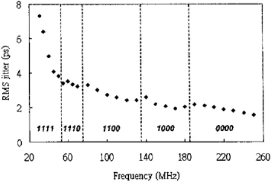
Fig. 12. Fig. 13 shows the measured mis jitter characteristics of the dual-loop DLL over different operating frequencies and corresponding digital control code words. The performance degradation at low operating frequency is due to clean low-frequency input reference clock not available especially below 45MHz. Table 1 summarizes the performance of the proposed DLL.
Q 40 c
Process Operating voltage Operating frequency range Output multi-phase clock rate
RMS jitter Peak-to-peak j itter Power dissipation Active area
\
-
-11101 +IO001-
-ww/
... ~;L~+““~
...
I 0.18-um 1P6M CMOS process 1.8v
25 MHz -250 MHz 0.8 GHz-
8 GHz 2.1 ps @ 125 MHz I .6 ps @ 250 MHz 14.9 ps @ 125 MHz 12.1 ps @! 250 MHz 1.6 mW @? 25 MHz 9.1 mW @, 250 MHz 0.2 m 2,
I I 2 1.4 I .6LOOP C0”tIOl “Oltage (V)
Fig. 10 Measured
transfer curve of
the delay line.Fig. 11 DLL output
jitter
histogram at 125MHz
(analog V,,= 1 . I V a n d digital
control
codeI?Oa).
Fig. 12 DLL output
jitter
histogramat
125 M H z when the digitalDLL
is
disabled(analog V,,=
1.1
V
and digital control code700~7).
5. ConclusionAn analog-digital dual-loop adaptive-bandwidth DLL is proposed to achieve a low-jitter characteristic over a wide operating kequency range and across PVT variations. The deterministic jitters induced by the unnecessary ripples on the loop control line are eliminated by employing the complementary phase detector (PD). The level-shifter circuit reduces the power consumption over the entire operating frequency 50% at lest by using a self-feedback technique. The output multi-phase clucks of the DLL achieve an equivalent sampling clock rate spanning from
0.8 GHz tu 8 GHz, which is sufficient for most UWB system applications. Because of the analog-digital dual- loop architecture, the proposed DLL can easily improve the performances such as operating frequency range and jitter characteristic with little extra hardware, which will benefit greatly from future scaling-down CMOS process.
![[2016-Fall] WNFA lab3 - JJY](data:image/gif;base64,R0lGODlhAQABAIAAAP///wAAACH5BAEAAAAALAAAAAABAAEAAAICRAEAOw==)