國 立 交 通 大 學
材料科學與工程學系碩士班
碩士學位論文
以準分子雷射退火改善於高分子基板上之氧化銦錫薄膜與基板對光
學能隙影響之探討
Investigations of Excimer Laser Annealing on ITO deposited on
polymer substrates and substrate effect on the optical band gap
shifting
研 究 生 :Dang Thi Thuy Chi
指導教授:呂志鵬 博士
以準分子雷射退火改善於高分子基板上之氧化銦錫薄膜與基板對光
學能隙影響之探討
Investigations of Excimer Laser Annealing on ITO deposited on polymer
substrates and substrate effect on the optical band gap shifting
研 究 生: 鄧氏垂芝 Student: Dang Thi Thuy Chi 指導教授:呂志鵬 博士 Advisor: Dr. Jihperng (Jim) Leu
國 立 交 通 大 學 材 料 科 學 與 工 程 學 系
碩 士 論 文
A Thesis
Submitted to Department of Materials Science and Engineering College of Engineering
National Chiao Tung University In Partial Fulfillment of the Requirements
For the Degree of Master In
I
Investigations of excimer laser annealing deposited on polymer substrates
and substrate effect on the optical band gap shifting
Student: Dang Thi Thuy Chi Advisor: Dr. Jihperng (Jim) Leu
Department of Materials Science and Engineering National Chiao Tung University
Abstract
For the development of flexible microelectronic device technology, indium-tin-oxide (ITO) on polymer substrates has attracted interest recent years. Therefore, development of a novel post treatment method to improve properties of ITO film without damage polymer substrate is an important key issue for successful application as a transparent electrode material.
In this study, a KrF excimer laser source has been used to anneal ITO deposited on polymer substrates, which are polyethylene terephthalate (PET) and ODPA-BADB polyimide (PI). The electrical and optical properties of ITO films following various laser shots number were further investigated. For microstructure, after laser irradiation, the ITO film from amorphous phase changes to crystalline phase. For room temperature ITO deposited on PET following laser irradiation, the ITO films show reduced surface roughness, 42% reduction of resistivity (4.3×10⁻⁴ Ω-cm) and enhanced carrier concentration of 5×1021 cm-3 (14 times increase). For higher
II
temperature ITO deposited on ODPA-BADB PI substrate at 200oC following laser irradiation, it shows very low resistivity, which around 3.2×10⁻⁴ Ω-cm.
The substrate effect on optical band gap shift of ITO films was also investigated. It has been shown that, the optical band gap of ITO film does not only depend on ITO films itself such as heavy carrier concentration and impurity, but also be affected by different substrates. The different in tensile stress induced by the ITO film and polymer substrate due to the different of coefficient thermal expansion (CTE) mismatch leads the optical band gap shift of ITO film.
III
以準分子雷射退火改善於高分子基板上之氧化銦錫薄膜與基板對光
學能隙影響之探討
研 究 生: 鄧氏垂芝 指導教授:呂志鵬 博士 國立交通大學材料科學與工程學系碩士摘要
近幾年在軟性微電子元件科技發展過程中,以沉積氧化銦錫薄膜於高分子 基材之技術引起了最多的研究興趣與關注。因此,發展一個新穎的後退火技術 用以改善氧化銦錫薄膜之特性同時不破壞高分子基板,對於其做為透明導電材 料是否能成功的應用於軟性電子是一個十分重要的議題。 在此研究中,我們使用KrF準分子雷射作為退火源,分別處理ITO薄膜於不 同的高分子基板(PET與ODPA-BADB PI)。經由雷射處理後它們的光、電等性質將進一步探討。微結構而言,雷射後 退火處理的ITO薄膜由初沉積的非晶相轉變為結晶相。對於室溫沉積於PET的IT O薄膜而言,經雷射退火,表面粗糙度下降、電阻率也下降了42% (4.3×10⁻⁴ Ω-cm) 並且增進14倍的载子濃度(5×1021 cm-3)。對於200 o C高溫沉積於ODPA-BADB PI的ITO薄膜而言,經雷射退火後,其電阻率更低,約為3.2×10⁻⁴ Ω-cm。 我們也探討基材效應如何影響ITO薄膜的光學能隙變化。實驗發現,ITO薄 膜的光學能隙不只有被薄膜本身的特性所決定(如過多载子濃度和缺陷等),基材IV
也是另一個決定的因素。結果指出,ITO薄膜與基材之間的熱膨脹係數差異會誘 發張應力,而進一步改變ITO薄膜的光學能隙。
V
ACKNOWLEDGEMENTS
First and foremost, I am indebted to my advisor Dr. Jihperng (Jim) Leu for his guidance, patience, and support throughout this research. He gave me the precious opportunity to coming to Taiwan and supporting my Master’s degree here.
I also owe a debt to many staff members and my fellow graduate students in this department. In particular, I would like to send my great thank to my senior PhD candidate Chih Wang for his helpful discussions. Special thanks to Hsin-Ling Hsu for her kindness help in both research and life. Thanks to all my lab-mates for their friendship which made my life in Hsin-Chu very enjoyable.
Last but not least, I wholeheartedly give thanks to my parents, my sister for their love, encouragement, understanding and support.
VI
Dedicated to my parents
for their endless love and encouragement
VII
Contents
Abstract ... I 摘要... III Acknowledgement……… V Contents ... VII Table Captions ... IX Figure Captions ... X Chapter 1 Introduction ... 1Chapter 2 Literature Review ... 5
2.1 General Theory of ITO film………..5
2.2 ITO on glass and flexible substrate ... 13
2.3 Why Excimer Laser Annealing ITO ... 14
2.4 KrF Excimer Laser irradiated ITO films ... 16
2.4.1 Laser-solid interaction ... 16
2.4.2 Excimer laser crystallization of ITO ... 16
2.4.3 Excimer laser annealing improved properties of ITO………...17
2.5 Applications of ELA for flexible substrate devices and others……...……....18
Chapter 3 Experimental ... 20
3.1 Sample praparation ... 20
3.1.1 Substrate preparation ………. .20
3.1.2 Indium Tin Oxide layer deposition………...22
3.2 KrF Excimer laser treatment... 24
3.2.1 KrF excimer laser system ... 24
3.2.2 Experimental procedure ... 26
3.3 Instrumentation ... 28
3.3.1 Grazing Incident X-ray Diffraction (GIXRD) ... 28
3.3.2 Hall effect measurement... 29
3.3.3 UV visible spectrophotometer system... 30
3.3.4 Atomic Force Microscopy (AFM) ... 30
3.3.5 Scanning Electron Microscopy (SEM)……….31
VIII
Chapter 4 Results and Discussion ... 33
4.1 Effect of ITO film on PET substrate under ELA ... 33
4.1.1 Structure of ITO film on PET under ELA ... 33
4.1.2 Effect of ELA on morphology of ITO/PET ... 35
4.1.3 Effect of ELA on electrical properties of ITO/PET ... 37
4.1.4 Effect of ELA on optical properties of ITO/PET………..40
4.2 Optimize properties of ITO on polyimide substrate by ELA ... 43
4.2.1 Structure of ITO/PI under ELA ... 43
4.2.2 Effect of ELA on electrical properties of ITO/PI ... 44
4.3 Effect of ELA on properties of ITO on free standing PET………...46
4.4 Substrate effect on optical band gap shifting………..49
4.4.1 Effect of ELA on stress behavior of ITO/PET……….49
4.4.2 Effect of ELA on optical band gap of ITO/glass………...52
4.4.3 Effect of different substrate on optical band gap of ITO films………53
4.4.4 Optical band gap of different thickness of ITO films………...55
Chapter 5 Conclusion and suggestions for future work ... 59
5.1 Conclusions………..59
5.2 Suggestions for future work……….60
IX
Table Captains
Table 2.1 Summary of properties of typical ITO films deposited using
various technique……….13
Table 2.2 Category of some lasers………..15
Table 3.1 Summary of sample parameters……….22 Table 3.2 Experimental parameters for ITO deposition………23 Table 4.1 Variation of crystalline size of ITO/PET with laser shots
irradiation……….34 Table 4.2 Different initial stress and band gap of ITO/PET with various
laser shots number………...51 Table 4.3 The carrier concentration and optical band gap of ITO/glass
under ELA………..52 Table 4.4 Properties of ITO on PET and PI substrates………...54 Table 4.5 Summary properties of different ITO thickness on different substrate....56
X
Figure Captions
Figure 1.1 The world-wide indium consumption……….1
Figure 1.2 Example of flexible photovoltaic display……….………2
Figure 2.1 Schematic representation of the ITO band structure……….……..10
Figure 2.2 Transmittance spectra of classic ITO film……….………..13
Figure 3.1 The chemical structure of PET………...20
Figure 3.2 The chemical structure of TFA………...…....20
Figure 3.3 The chemical structure of ODPA……….21
Figure 3.4 The chemical structure of BADB……….21
Figure 3.5 PVD sputtering system for the ITO deposition………..23
Figure 3.6 KrF Excimer laser system for irradiation………....24
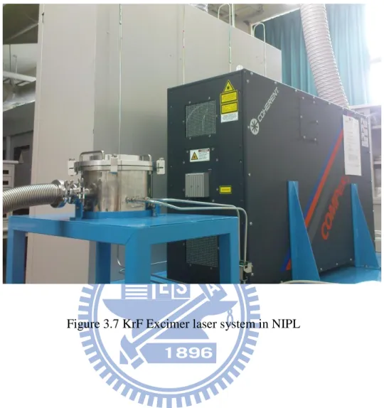
Figure 3.7 KrF excimer laser system in NIPL………...25
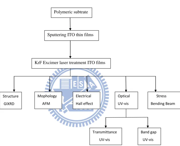
Figure 3.8 Flow-char of experimental procedures………....27
Figure 3.9 Grazing Incident X-ray Diffraction……….28
Figure 3.10 AFM basic work diagram……… 30
Figure 3.11 Unstressed and stressed structure of film and substrate……… 32
Figure 4.1 GIXRD pattern of ITO/PET under various laser shots irradiation……….33
Figure 4.2 Surface roughness of ITO/PET under ELA………....35
Figure 4.3 SEM cross-section of ITO/PET………36
Figure 4.4 Resistivity of ITO/PET as a function of laser shots number………37
Figure 4.5 Carrier concentration of ITO/PET as a function of laser shots number….38 Figure 4.6 Mobility of ITO/PET as a function of laser shots number ……….40
Figure 4.7 Optical transmittance spectra for ITO/PET under ELA………...41
XI
Figure 4.9 GIXRD spectra of ITO/PI under ELA……….43
Figure 4.10 Resistivity of ITO/PI under ELA……….44
Figure 4.11 Carrier concentration of ITO/PI under ELA………..45
Figure 4.12 Mobility of ITO/PI under ELA………...46
Figure 4.13 Resistivity of ITO on free standing PET under ELA……….47
Figure 4.14 Mobility of ITO on free standing PET under ELA………...47
Figure 4.15 Carrier concentration of ITO on free standing PET under ELA………..47
Figure 4.16 Transmittance spectra of ITO on free standing PET under ELA……….48
Figure 4.17 Thermal stress vs temperature of ITO/PET………49
Figure 4.18 Effect of laser shots on stress behavior of ITO/PET……….…50
Figure 4.19 Effect of ELA on optical band gap of ITO/glass………...52
Figure 4.20 Optical band gap of ITO on PET and PI substrate………53
Figure 4.21 Optical band gap of 140 nm ITO on different substrate………55
1
Chapter 1 Introduction
1.1 Background
Indium-tin-oxide (ITO) has been widely used as transparent electrodes in many optoelectronic applications, especially displays due to its high electrical conductivity combined with high transmission in the visible spectra. The use of ITO in display has quickly grown to become the primary end user of the world’s indium production as illustrated in Figure 1.1 [1].
ITO thin films that commonly were deposited on glass substrates have been used as the transparent conducting electrodes in many optoelectronic devices, such as flat panel displays and photovoltaic devices. This is because of their superior conductivity and high transparency [2-6]. However, glass substrates are unsuitable for certain applications where flexibility, light weight and toughness are needed because glass is brittle, heavy and not deformable. In order to overcome these disadvantages, flexible substrates, which are made of plastic, have been used instead of glass [7-11].
Recently, flexible microelectronic devices such as flexible organic emitting diode (FOLED), e-paper, flexible solar cell and liquid crystal display (LCD) have
Figure 1.1 The world-wide indium consumption. The majority of indium used in thin film application is the display industry [1]
2
emerged as popular personal devices [12,13] for its light weight, toughness, and mobility. ITO films on polymer substrates have been widely used as transparent electrodes in these devices [12,13].
Figure 1.2 Example of flexible photovoltaic display [reference] However, polymers pose three distinct challenges. First, ITO is often annealed at 200-250 oC to achieve both low resistivity and high transparency, but low Tg (glass
transition temperature) of common polymer substrates, e.g. polyethylene terephthalate (PET) constrains the maximum processing temperature in the fabrication of flexible devices. Second, the properties of ITO films on polymer tend to be worse due to low processing temperature or poor nucleation [14]. Thirdly, ITO thin films on polymer substrate also show mechanical limitation. Currently, there are several polymer substrate candidates suitable for ITO deposition at or near desired high temperature, 300 oC. However, along with the temperature capabilities of the polymer substrate, its shrinkage or expansion with temperature, i.e. coefficient of thermal expansion (CTE) must be considered for its suitability and compatibility of use with ITO [15] and other transparent oxide in optoelectronic devices. When deposited onto flexible polymer substrates, cracking, delamination, or buckling of ITO have been reported.
3
Thus, it is necessary to develop a low thermal budget annealing technique to improve the properties of ITO films deposited onto the polymeric substrate. It has been shown that excimer laser annealing (ELA) technique is powerful technique as a post treatment method for flexible substrate with several advantages [15]. Firstly, ELA technique takes only 25 ns to render ITO phase transformation, whose time scale is ten orders of magnitude quicker than the conventional furnace annealing. Secondly, ELA offers much shorter thermal diffusion length and thus enables post-anneal of flexible devices at room temperature.
In hope to address the challenges of ITO on polymers substrates from the point view of ELA method, the objectives of this thesis are the following:
1. To establish low temperature laser annealing technology of transparent conducting oxide for flexible device applications
2. To investigate the effect of ELA on the properties of ITO onto polymer substrates
3. To study the effect of polymer substrate on the optical bandgap of ITO films In specific, a KrF excimer laser was used to treat the ITO films sputtered onto polyethylene terephthalate (PET) and polyimide (PI) substrates. The microstructure, electrical, optical, and mechanical properties of ELA-treated ITO films were examined. Excimer laser parameters were carefully optimized to ensure the resistivity, carrier concentration as well as transmittance of ITO films are comparable to those deposited at high temperature (>200oC) on the glass substrate. Besides that, the mismatch of CTE and elastic modules between ITO film and polymers may induce thermal stress at the interface. We plan to explore the impact of the thermal stress from the mismatch of CTE and E on the ITO properties such as optical bandgap and
4
xxx. Moreover, the substrate effect on ITO films with different thickness and deposited on different polymeric substrates will be examined.
1.1 Outline of this thesis
The aim of this thesis is fabrication and treatment ITO on polymeric substrates without deteriorating the high electrical and optical performance commonly achieved, and to create an understanding of the fundamental aspects in order to optimize and develop these materials. This thesis was organized into five chapters. Following a concise introduction in Chapter 1, Chapter 2 will review the general properties of ITO and introduce the ELA method as well as its application for flexible devices. Chapter 3 describes the sample preparation and instrumentation. Chapter 4 describes the properties of ITO on polymeric substrate under KrF excimer laser irradiation. Then the results and conclusion of this thesis are summarized in Chapter 5.
5
Chapter 2 Literature review
2.1 General theory of ITO
2.1.1 Electrical properties
ITO thin film is n-type degenerate polycrystalline material. It has a cubic bixbyite structure [15]. Basically, its electrical resistivity ( ) depends on the carrier concentration (N) and mobility of the relevant free carrier
where e is the electronic charge and µ is the mobility which can be expressed as
where , , and are the mobilities corresponding t lattice vibration scattering [16], ion impurity scattering [16,17], neutral impurity scattering [16,17], and grain boundary scattering [18,19], respectively.
The electron carriers of ITO film can be generated by the tin dopant [15] and by oxygen vacancies [15,16]. Tin acts as a cationic dopant when it substitutes indium and is surrounded by In2O3. It provides an electron to the conduction band. Using the
Kroger-Vink notation this reaction can be described as:
Theoretically, the maximum carrier density by tin doping is , where
is the tin concentration (at %) [15]. Consequently, at low Sn weight ratio the
resistivity decreases with Sn concentration in accordance with Eq (2-1) [20]. It is well known, however, that increasing the Sn weight ratio above 5% leads to a saturation in resistivity and then to a slight increase in resistivity [17,20]. Above this Sn concentration the carrier concentration of ITO thin film is found to be essentially
6
constant. Several hypothesis have been made to account for this behavior [15.17.20-22]: (i) when one of the nearest-neighbor In2O3 sites around tin ion is occupied with a
second tin ion the donor action is compensated. (ii) If excess Sn doping occupies an interstitial site then it forms a deep level electron trap rather than an electron donor. (iii) Some other reason exists for Sn being electrically inactive.
Apart from the Sn doping, oxygen vacancies can act as doubly ionized donors contributing up to two electrons to the conduction band.
The effect of the oxygen vacancy is more complex since they also influence ion impurity scattering mobility through the presence of O2- [15]. When oxygen vacancies have a high enough concentration they form an impurity band which overlaps with Ec
(bottom of conduction band) that makes the ITO thin film an n-type degenerate semiconductor.
In order to increase the carrier concentration and thereby improving the electrical conductivity, most effort has focused on two research directions. The first is to develope improved methods of doping (such as ion implantation) [16, 22-26]. The second has involved the variation of preparation conditions [18, 21, 27-33]. For the first direction, various ions are implanted into either In2O3 or ITO and the
improvements in the electrical conductivity is sought. In the case of tin implantation into In2O3 [34], the resistivity of the film decreases and the intensity of the XRD peak
corresponding to (440) plane as well as its width increase with tin dosage. For In+ ion implantation into ITO film, an increase in carrier concentration is observed, which is attributed to the generation of more vacancies and stabilizing excess oxygen vacancies [25]. However, Sn, which can not contribute carriers in the ITO amorphous phase produced on implantation, is found to require post annealing [15, 17]. For H+ ion
7
implantation, Serikawa and Shirai found improved conductivity due to an increase carrier density and suggested that this was due to the formation of charged oxygen vacancies [35]. Shigesato et al, however, argued that this improvement results from the improved crystal quality due to annealing effect and neither O+ nor H+ implantation formed oxygen vacancies for contributing carriers [16]. Lee et al, reported that arsenic and boron implantation did not improve resistivity [36].
There have many efforts to improve electrical conductivity through better ITO film preparation procedures. Both the choice of deposition parameters and the post-treatment conditions play an important role in determining the carrier concentration. As mentioned above, both the tin doping content and the density of oxygen vacancies contribute to the carrier concentration. The tin content depends not only on the Sn weight ratios used in the evaporation or sputter sources [17, 20], but also on the various preparation conditions [37]. Sn dopant is totally inactive in amorphous material, but as the crystalline state of ITO film improves so the effectiveness of the dopant in releasing carriers increases [16, 17]. Varying depositions and post annealing parameters play an important role in the contribution of the oxygen vacancies [21].
As noted from Eq (2-1), the electrical resistivity is influenced by two factors: the carrier concentration and the mobility. Honda et al, [38] and Banerjee et al, [39] mentioned that electrical conductivity can be improved by increasing the carrier mobility. However, the carrier mobility and concentration are interdependent being governed by a rule [15]. For the highest electrical conductivity, there must then be a trade-off between the carrier concentration and the mobility. As mentioned above, increasing the Sn content above 5% causes no increase in the carrier concentration. The added Sn results in the formation of deep electron trapping centers which in turn tend to reduce the mobility of free electrons and lead to a reduced
8
conductivity. As expressed by Eq (2-2), the mobility is influenced by various scattering mechanisms. Kikuchi at al reported that phonon scattering was one of the dominant electron scattering mechanisms limiting the carrier mobility in highly conductive as-deposited ITO films produced by DC sputtering [40]. This was in agreement with the work of Zhang and Ma [41], who found that while ionized impurity scattering dominated in the low temperature range indicated for transparent conducting ITO, longitudinal phonon scattering was the main scattering mechanism in the high temperature range, which is expressed in Eq (2.5) [41]
Where is the elasticity constant modulus, is the divergence of train, h is
Plancks’s constant, k is the Boltzmann’s constant, T is the absolute temperature, is the effective mass of electrons and in the degenerate ITO system.
Ionized impurity and neutral impurity scattering are the important scattering mechanisms in a degenerate semiconductor with high carrier density [16]. The contribution of these scattering mechanisms to conductivity was theoretically evaluated by Erginsoy [42], Conwell and Weisskopf [43], as well as Dingle [44]. These theories have been used by many authors [15, 17, 45, 46] to describe the effect of neutral and charged carrier scattering in ITO. The expression for neutral scattering may be expressed as:
The expression ionized impurity scattering is described by Eq (2.7)
9 Where the screening function g(x) is given by
where
Where is the permittivity of free space, is low frequency relative permittivity, Z is the charge of the ionized centers. For ITO film the value of and, are respectively taken as 0.3 and 9 [15, 17, 46, 47]. The interaction of scattering centers and/or formation neutral scattering defects should be taken into account when the mobility is relatively low in high doping concentration ITO film [15].
Domain boundaries act as a barriers obstructing free carrier motion so that material with larger grain size is in general preferred to increase carrier mobility. The importance of grain boundary scattering effect on the carrier mobility in ITO films, however, is still an open question. For example, it is found that the sheet resistance drops with increasing grain size [48]. However, from these studies it is not clear whether the improved electrical conductivity results from reduced grain boundary scattering or reduced oxygen vacancy scattering, since both of these correlated with improved stoichiometry. The mobility corresponding to grain boundary scattering can be expressed as [38]:
Where l is grain size and is the grain boundary potential barrier. Mean scattering lengths for ionized impurity and neutral scattering have been given by a number of research groups. For example, Maivannan and subrahmanyam [27] reported a mean scattering lengths of 4-6nm, while Shigesato et al, values of 2-8 nm [16]. For most ITO films, the grain size is typically an order of magnitude larger than this so that
10
grain boundary scattering, while making some contribution to the carrier mobility, is unlikely to be dominant in most films.
2.1.2 Optical properties
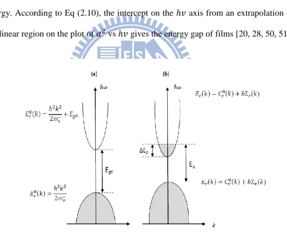
The wavelength dependent transmittance and absorption can be used to estimate the optical energy band gap. Its value can be calculated from the absorption spectra using the following equation (2.10) [49]
)
where is the absorption coefficient, is the optical band gap, and is the photon energy. According to Eq (2.10), the intercept on the axis from an extrapolation of the linear region on the plot of vs gives the energy gap of films [20, 28, 50, 51].
11
However, Manivannan and Subrahmanyam [27] as well as Hamberg and Granqvist [52] have argued that this technique is not valid for a heavily doped semiconductor. They suggest that a broadening parameter should be introduced to take into account electron-electron interactions and impurity scattering. However, there is not yet a consensus on this matter since some authors do not agree with the revised theory [53]. This makes the determination of any accurate absolute value for difficult at the present time.
The band structure of ITO is approximated by parabolic functions of k close to the band edges. The schematic representation in Fig. is valid for most binary metal oxide wide band gap semiconductors. The valence band maximum and conductions band minimum are both located at k=0, so the material is said to be a direct band semiconductor.
The direct optical band gap of ITO films is generally greater than 3.75 eV although a range of values from 3.5 to 4.06 eV have also been report in the literature [54, 55]. It is well know that for ITO films the optical and electrical properties are interdependent [27]. The optical band gap is influenced by carrier concentration in two following aspects:
(1). The increase in optical energy broadening is due to an increase in carrier concentration. Many experimental results [27, 56] show that the edge of transmittance shifts to the shorter wavelength side with increasing carrier concentration. When the carrier concentration increases and the Fermi level shifts to higher energy in a more heavily doped n-type semiconductor [57-59] the optical energy band gap increases. This is referred as the Burstein-Moss shift [60] and is given by Eq (2.11)
12
Where is the intrinsic energy gap and is the reduced effective mass and given by Kim et al, as [20]
Where and are the effective masses of carriers in the conduction and valence bands respectively. The Burstein-Moss shift increases when low lying energy levels in the conduction band fill up. A wide range of experimental values 2.98-3.75 eV of the intrinsic absorption edge have been reported together with a wide range of carrier effect masses for ITO films deposited using different conditions and techniques [61, 65]
(2) When the carrier density very high the phenomenon of band gap narrowing [11, 56] is attributed to electron-electron and electron-impurity scattering [17]. Kim et
al, reported that the absorption edge shifts to the lower energy side under Sn doping
[20]. Thus, with this effect taken into consideration one writes [43]
Where are the self energies due to electron-electron and electron-impurity scattering. To further complicate this picture, in addition to the previously mentioned effects (1) and (2), the value of also varies with crystal orientation [18, 65] and oxygen content [56, 65]. For example, Thilakan and Kumar reported that the values of the optical energy for the (222) and (400) orientation planes are 3.83 eV and 3.26 eV respectively [65].
13
2.2 ITO on glass and flexible substrate
To improved the properties of ITO on glass, we can use many methods either in both pre-deposition or post-deposition. A summary of electrical and optical properties of typical ITO films deposited using various techniques are summarized in Table 2.1. Variations in film properties can be easily noted. Their differences are attributable to both pre-deposition and post- deposition treatments as well as the techniques themselves.
Table 2.1. Summary of properties of typical ITO films deposited using various techniques Deposition technique Thickness [Anstron] Hall mobility [cm2/s] Carriers [cm-3] Resistivity [Ωcm] Transmittance [%] Ref No r.f sputtering 7,000 35 6x10²⁰ 3x10⁻⁴ 90 [66] r.f sputtering 5,000 12 12x1020 4x10⁻⁴ 95 [67] Magnetron sputtering 4,000 26 6x10²⁰ 4x10⁻⁴ 85 [68] d.c sputtering 800 35 9x10²⁰ 2x10⁻⁴ 85 [69] Reactive Evaporation 1,000 30 5x10²⁰ 4x10⁻⁴ 91 [58] Ion Beam Sputtering 600 26 2x10²⁰ 12x10-4 [70]
At present, the use of ITO on polymer substrate for flexible optoelectronic application has become significant in the field of research. However, the properties of ITO films on polymer substrate tend to be worse due to low processing temperature or poor nucleation [13].To overcome such constraint in processing temperature, ITO film
14
on polymers involve most approached for optimizing the quality of pre-deposition method such as working pressure, gas ratio, target composition, etc [71, 72, 73]. Besides that, in case of some high glass temperature (Tg) polymer such as Polyethylene naphthalate (PEN) and polyimide (PI), properties of ITO films can be improved by high deposition temperature or thermal annealing [74]. However, high Tg polymer substrate are often high cost and most of polymer could not be annealed to above 300oC , which is still well below the required annealing temperature ITO, 400oC.
2.3 Why Excimer laser annealing ITO
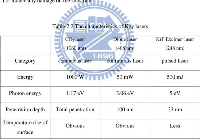
Laser annealing is a powerful technique for flexible devices. Effect of laser on materials depends on laser type and laser wavelength. Figure 2.2 is a transmittance spectrum of classic ITO on glass.
Comparing the transmittance of different laser wavelengths, photon from diode laser (405 nm) and CO2 laser (1060 nm) are mostly transmitted in ITO film, while the
photon of KrF excimer laser is completely absorbed. Such energy excites electron
500 1000 1500 2000 0 20 40 60 80 100 ITO film T% Wavelengh (nm) KrF laser (248nm, 5eV) Diode laser (405nm, 3.06 eV) CO2 laser (1060nm, 1.17eV) Band gap of ITO is ~3.8eV
Figure 2.2 Transmittance spectra of classic ITO film cckjhefiuccccclac\\\\\\\\\\\\\\\\\\glass
15
from valence band jump up to conduction band of ITO film hence enhance ITO electrical properties. The energy of a photon is calculated by , where =6.626 x 10⁻³⁴ Js is the Planck’s constant, c= 3.00 x 10⁸ m/s is the speed of light, and is the wavelength of incident photon beam. Based on this equation, the photon energy from KrF excimer laser is 5 eV, which is larger than the band gap of ITO films (3.7eV). This is the first advantage of KrF excimer laser compared with other lasers. The characteristics of key lasers are summarized in Table 2.2. The temperature rise of surface ITO by using KrF excimer laser is much less than CO2 laser and diode laser.
Due to the penetration depth shorter, the pulsed UV laser beam (duration 20 ns) does not induce any damage on the substrate.
Table 2.2 The characteristics of Key lasers CO2 laser (1060 nm) Diode laser (408 nm) KrF Excimer laser (248 nm) Category continuous laser continuous laser pulsed laser
Energy 1000 W 50 mW 500 mJ
Photon energy 1.17 eV 3.06 eV 5 eV
Penetration depth Total penetration 100 nm 33 nm Temperature rise of
surface
16
2.4 KrF Excimer laser irradiated ITO films
2.4.1 Laser-solid interaction
Absorption of incident energy fundamentally dictates the resultant thermal state of the material and therefore is a suitable point to begin an analysis of laser – solid interactions. The mechanisms involving absorption of incident radiation in materials are defined by the electronic structure of the materials. Therefore it is useful to discuss exclusively semiconductors. In semiconductors, five distinct mechanisms for the absorption of light can be identified [75]
1) Photons with energy (hv) much less than the band gap energy (Eg) can excite
lattice vibrations directly.
2) Free or nearly free carriers can be excited by absorption of light with hv<Eg ;
such carriers will always be present as a result of finite and doping
3) An induced metallic-like absorption due to free carrier generated by the laser radiation itself can occur
4) For photon energies are larger than Eg, absorption will take place by direct
and indirect (photon-assisted) excitation of electron-hole pairs
5) Absorption induced by broken symmetry of the crystalline lattice is possible When a beam of photons of energy hv > Eg is absorbed in a semiconductor,
excited carriers, which results in lattice heating [76], is a complicated process and an field of active research [77].
2.4.2 Excimer laser crystallization of ITO
The basic mechanism of laser heating process is through photon absorption and the subsequent rapid transfer of energy from the electrons to the lattice [78-80]. During laser annealing, a beam of photons is focused on a sample. The photons
17
interact with the electrons in the sample which then transfers the energy to the lattice. This causes localized heating in the area where the photons hit the sample. More specifically, the wavelength of this light determines how the energy will be absorbed in the ITO. The energy of the laser beam, or incident photon energy, is determined by the equation:
With h equal to Planck’s constant, c equal to the speed of light and λ equal to the wavelength of the laser. With the band gap of ITO around 3.7 eV, laser energy greater than this band gap results in absorption via band to band transitions, which results in the desired heating of the region. When the heating is sufficient, phase transitions may occur.
2.4.3 Excimer laser annealing improved properties of ITO
Because of inducing crystallization, the excimer laser also improved properties of ITO films. When ITO film becomes crystalline, the resistivity will be reduced due to the ordering and re-arrangement in structure. Besides that, when an oxygen atom becomes a part of the indium oxide lattice, two In-O bonds are created, which requires two electrons coming from the conduction band to fall in the valence band. Under UV exposure, hv > Eg, many carriers are promoted in the conduction band. Some In-O
bonds are broken and oxygen atoms can escape to the gas phase. When UV exposure stops, most of the carriers fall back again in the valence band. But, as oxygen atoms are missing in the lattice, there is lacking states in the valence band. Some carriers must stay in the conduction, leading to an increase in carrier concentration. The large increase of carrier concentration after KrF excimer laser exposure could be a sign that some oxygen atoms are also desorbed from the bulk [81]. Moreover, under KrF
18
excimer laser annealing, the carrier concentration of ITO film increases also because of the substitution of Sn4+ to In3+ in In2O3 lattice due to thermal excitation. [82]
2.5 Applications of ELA for flexible substrate devices and other
applications
High temperature processing steps such as thermal annealing that are incompatible with plastic substrates are still a major hindrance. Laser annealing permits localized energy input without affecting the underlying substrate and can help overcome this problem.
In semiconductor technology, laser crystallization has been widely used for advantages of selective absorption and low substrate temperature. Moreover, the scanning area can be freely selected without heating other regions. The adoption of this technique can incorporate the fabrication of ferroelectric thin films into large scale integrated circuit processing and make mass production possible. For example, the ferroelectric perovskite phase in PbZr0.44Ti0.56O3 (PZT) films on glass substrates were
carried out by using laser annealing [83]. This work has made the processing of ferroelectric films compatible with Si integrated circuit technology. The other advantage of laser annealing technique is that ferroelectric films with random patterns can be made without heating other parts of device due to the controllability of the scanning laser spot. Several reports also have been presented on the study of the laser annealing of Pb(Zr, Ti)O3, PZT, PBTiO3(PT) thin films. The reported data on these
materials showed that the thin films could be crystallized at a low temperature [84]. In industry, production of low temperature p-Si back plates for LCD by high power excimer laser annealing was introduced several years ago. Regarding the economy of the process, one of the major advantages of excimer laser annealing is the
19
opportunity to make use of low cost glass substrates due to the low temperature of the annealing process [85]
Beside two excellent major advantages of selective absorption and low substrate temperature of excimer laser annealing technique, the improvement of properties of materials induced by excimer laser irradiation is presented. For example, significant improvement electrical properties of TCO materials, patterning TCO are reported [86]. Moreover, the excimer laser irradiation induced phase transformation between anatase and rutile phase of TiO2 have important application for solar cells. In addition,
good dielectric properties of Pb(Zr,Ti)O3, PZT, PbTiO3(PT) thin films obtained after
20
Chapter 3 Experimental
3.1 Sample preparation
3.1.1 Substrate preparation (1) Preparation of thin PET film
Polyethylene terephthalate (PET) CAS No. 25038-59-9 PET particle: product by Nan Yan Plastic corporation
PET particle was dissolved in trifluoroacetic acid (TFA) solvent to form a 5 wt% solution, which was then stirred for 2 days. Afterwards, PET thin films of 3µm thickness were prepared by spin-coating on glass substrate and drying out the solvent in vacuum oven for 2 hours at room temperature.
(2) Preparation of free-standing film
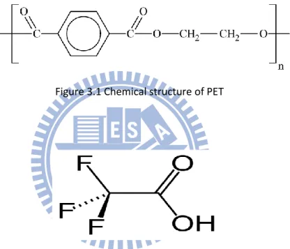
Free-standing film: product by Nan Ya Plastics Corporation, thickness 120 µm Figure 3.1 Chemical structure of PET
21
A free-standing PET thick film with a nominal thickness of 120 µm was cut into 1cmx1cm. Afterwards, the PET film was cleaned by acetone, DI water, and then baked at 60oC for 2 hours.
(3) Preparation of thin PI film [100]
Polyimide films were synthesized from dianhydride monomer 4, 4’- Oxydiphthalic anhydride, 97% ODPA and - Bis(4-aminophenyl)-1,4-diisopropylbenzene ODPA. In the synthesis, BADB was first added in the DMAc and stirred at the room temperature until BAPP was completely dissolved.
Figure 3.3 Chemical structure of ODPA
Figure 3.4 Chemical structure of BADB
Then, ODPA was added into the solution and stirred for 1-2 days to prepare a highly viscous solution. Then poly (amic acid) solution was spin-coated on glass substrate and heated in an oven from room temperature to 2700C to form a polyimide film with a thickness of 3 µm.
22 (3) Substrate preparation for bending beam test
Each polymer (PET and PI) was spun onto double polished 5x5 cm2 Si wafer with film thickness of 3 µm. This wafer will be cut into 5 pieces of 1x5 cm2 stripers. 3.1.2 Indium Tin Oxide layer deposition
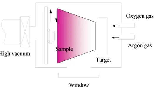
Indium tin oxide (ITO) thin films were deposited onto these polymer substrate at room temperature (RT) and 200oC with different thickness 50nm and 140nm by sputtering ceramic ITO target. The sample details shows in Table 3.1. The schematic diagram of the physical-vapor-deposition (PVD) sputtering system was illustrated by Figure 3.2. In general, ITO film should have (1) good optical transmission, (2) low stress in the film, (3) good thickness uniformity, and (4) low sheet resistance. The deposition parameters that affect the above characteristics of the ITO film were identified as (1) temperature of the deposition chamber, (2) total gas flow, (3) power, and (4) oxygen percentage in Ar.
Table 3.1 Summary of sample parameters
ITO parameters Substrate
Thickness: 140nm
Deposition temperature: RT
PET/glass, PI/glass, PET/ Si, PI/Si, glass, free-standing PET Thickness: 140nm Deposition temperature : 200oC PI/glass Thickness: 50nm Deposition temperature: RT PET/glass, PI/glass
23
Deposition parameters Conditions
DC power 1000 W
Base pressure 5 x 10⁻⁶ Torr
Working pressure 2.74 mTorr
Argon flow rate 300sccm
Oxygen flow rate 5 sccm
Thickness 140nm, 50nm
Substrate temperature RT, 200oC
Figure 3.5 PVD sputtering system for the deposition of ITO films
24
3.2 KrF Excimer laser treatment
3.2.1 KrF Excimer laser system
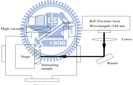
Laser annealing was performed using a Lambda Physik Complex 201 excimer laser operating at 248 nm (KrF) and pulse width 25 ns (FWHM). Energy of source was varied in the laser control system to alter the beam energy and hence the energy density on the sample. Frequency of laser was also adjusted to change the number of pulses per unit time. The duration of laser treatment was measured by timer. The schematic diagram and experimental set up in this study are illustrated in Figures 3.4 and 3.5, respectively. Stage Annealing sample Raster Lence Wavelength=248 nm KrF Excimer laser Ar,O2 Window High vacuum
25
26 3.2.2 Experimental Procedures
Experimental procedures in this study are outlined by the Flow-chart illustrated in Figure 3.8. A KrF excimer was applied to anneal films, which were sputter deposited onto specified substrates (glass, PET, PI). Hall effect measurement was used to investigate electrical properties of ITO films. The structure of ITO films was determined by grazing incident X-ray diffraction at NSRRC. The morphology of irradiated ITO films was studied by atomic force microscopes. The UV visible spectroscopy was used to define the transmittance and band gap of ITO films. Moreover, to clarify the behavior of band gap, the bending beam test was used to measure the stress of ITO films on polymer substrates
The fundamentals of analytic instrumentation such as GIXRD, Hall effect measurement, UV-vis, AFM, bending beam test will be briefly described in the following sections.
27 Polymeric subtrate
Sputtering ITO thin films
KrF Excimer laser treatment ITO films
Structure GIXRD Mophology AFM Electrical Hall effect Optical UV-vis Stress Bending Beam Transmittance UV-vis Band gap UV-vis
28
3.3 Instrumentation
3.3.1 Grazing Incident X-ray Diffraction
Grazing incidence X-ray diffraction typically from a crystalline structure, uses small incident angles for the incoming X-ray, so that diffraction can be made surface sensitive. It is used to study surfaces and layers because wave penetration is limited. The penetration depth is in the order of nanometers. Below of the critical angle (typically 80%) of the surface material studied, an evanescent wave is established for a short distance and is exponentially damped. Therefore, Bragg reflections are only coming from the surface structure.
An advantage of GIXRD is that the electric field at the critical angle is amplified locally by a factor of four, such that the GIXRD signal is stronger.
The ITO films were scanned by synchrotron beamline 17B1 at National Synchrotron Radiation Research Center in Hsinchu, Taiwan (NSRRC). Because of the limited penetration depth of KrF excimer laser to ITO films, GIXRD is the best choice to see the structure of ITO films change under laser irradiation.
29 3.3.2 Hall effect measurement
Hall effect refers to potential difference (Hall voltage) on opposite sides of a thin sheet of conduction or semiconducting materials through which an electric current of flowing, created by a magnetic field applied perpendicular to the Hall element.
From the Hall effect measurements, the following properties of the materials can be obtained
(1) The sheet resistance, from which the resistivity can be inferred for a sample of a given thickness
(2) The doping type (p-type or n-type) material
(3) The sheet carrier density of the majority carrier (the number of majority carriers per unit area). Density of the semiconductor (doping level) can be found for a sample with a given thickness
(4) The mobility of the majority carrier Taking measurements
(1) Current IAB is a positive DC current measured in amperes (A)
(i) Injected into contact A (ii) Take out of contact B (2) Voltage VCD is a DC voltage (V)
Measure between contacts C and D with no externally applied magnetic field (3) Sheet resistance Rs is measured in Ohms (Ω)
Ohm’s Law
Obtain more precise measurements by taking several reciprocal measurements and averaging.
A B
30 3.3.3 UV visible spectrophotometer system
An analytical technique for the measurement of wavelength-dependent attenuation of ultraviolet, visible and near-infrared light and used in the detection, identification and quantification of atomic and molecular species. UV/VIS spectrophotometry was used to determine the absorption or transmission of UV/VIS light (180 nm to 900 nm) by a sample. It could also be used to measure the concentration of absorbing materials based on developed calibration curved of the material. From the absorption spectra, the band gap of material can be also determined.
3.3.4 Atomic Force Microscopy (AFM)
AFM enables characterization of local surface structures. It employs a tip on the end of a cantilever and record cantilever deflection variation. The tip can be bent by a repulsive
Figure 3.10 AFM basic work diagram
force between the tip and the sample. There are three operation modes, namely contact mode, non-contact mode and tapping mode. The contact-mode is the most common
31
method of operation for the AFM. The tip moves very close to the sample surface and scans horizontally across a small area. Fig 3.7 illustrates how this works; as the cantilever flexes, the light from the laser is reflected onto the split photo-diode detector. A monitor records the spatial variation produced by the tip-sample repulsive force or the tip height variation. The variation in the bending of the cantilever can be detected by the different signal. A plot of the laser deflection versus tip position on the sample surface provides the resolution of the topography of the surface.
3.3.5 Scanning Electron Microscopy (SEM)
SEM is a powerful microscopy method for close viewing of nanoparticles. The microstructure of TiO2 films was studied by a scanning electron microscopy (SEM,
HITACHI-S2500 JSM-6500F). The TiO2 film was coated on normal glass for easier SEM
sample preparation. The porous TiO2 film was observed by SEM including nanoparticle TiO2
film and light-scattering layer. And the film thickness also defined by SEM observation.
3.3.6 Bending beam system
The bending beam is used to measure the curvature (R) of the sample and thereby the thermal stress ( ) based on Stoney equation as illustrated in Eq 3.1 [101]
where 1/R: curvature of the substrate with film
1/R0: curvature of the bare substrate
: substrate biaxial modulus
ts, tf : substrate thickness and film thickness, respectively
Limitation: tf << ts
Because the different E and CTE of two thin film layers the stress of these thin films will change after annealing.
32
of two thin film layer the stress of these thin films will change after annealing. In this thesis, the bending beam system was used to determine the critical stress of ITO film on polymer substrate.
(a) (b)
33
Chapter 4 Results and Discussion
4.1 Effect of ELA on properties of ITO on PET substrate
4.1.1 Structure of ITO film on PET under ELA
ITO film on PET substrate was irradiated by a KrF excimer laser with a fluence of 40 mJ/cm2, frequency of 5 Hz, and different of laser shots from 1500 shots to 3000 shots. Structure of ITO films is determined by GIXRD with incident angle of 0.5. The microstructure of the ITO films becomes more crystalline with the increasing number of laser shots as shown in Figure 4.1. The GIXRD pattern also shown a strongly (222) preferred orientation of ITO material.
Figure 4.1 GIXRD patterns of the ITO/PET films under various laser shots irradiation
Based on the crystallization kinetics [87], the increased phase transformation of ITO films can be attributed to the accumulated energy well above the activation energy with increasing number of laser shots. The KrF excimer laser beam includes photons with an energy of 5 eV, which is larger than the fundamental band gap Eg of ITO (3.7
eV). This leads to the absorption of lights occurs. The excited electrons, whose kinetic
20 25 30 35 40 45 50 Virgin ITO ELA-1500 shots ELA-3000 shots In te ns ity ( a.u .) 2 (degree) (222)
34
energy ∆E >1 eV can move in the lattice and transfer their energy to other electrons and excite them to become next excited electrons. Besides that, atoms and lattice can also receive directly energy from the photons beam and start vibrating. Therefore, the interaction between light and matter is a combination of various processes including electrons, atoms (or vacancies) and phonons. These result in heating of the lattice. When the energy absorbed in the irradiated area supplies sufficient heating to the sample, phase transitions may occur.
Sample ITO/PET Peak position (degree) Lattice constant (nm) Crystalline size (nm) Virgin 31.66 0.148 1.99 3000 shot irradiated 31.70 0.147 2.00 1500 shot irradiation 31.88 0.146 2.08
The intensity of 3000 laser shots irradiation ITO was highest compared with 1500 laser shots treatment and virgin ITO films. This indicated that irradiation with higher number of laser shots yields higher crystalline ITO films. The average crystallite size of film has been calculated using the Scherrer’s formula [102]:
where are X-ray wavelength, the Bragg’s diffraction angle and the full width at half maxima (FWHM) of the peaks corresponding to the value respectively. The
Table 4.1 XRD peak positions, d-spacing and crystalline size of ITO/PET with various laser shots
35
values of , of the GIXRD peaks are estimated by Gaussuan fitting. The average crystallite sizes of the films under different laser shots irradiation are listed in Table 4.1. The crystallite size is found to increase from 1.99 nm to 2.08 nm as the number of laser shots treatment increased from un-irradiation to 3000 shots irradiation.
4.1.2 Effect of ELA on morphology of ITO/PET
The surface roughness ( Rrms) of ITO films on PET were shown in Figure 4.2.
Figure 4.2 Surface roughness of ITO films (a) non-irradiated, (b) 1500 laser shots irradiated, (c) 3000 laser shots irradiated
(a) (b)
36
The surface roughness are 1.19 nm, 1.17 nm and 0.9 nm for as-received and samples irradiated with 1500 shots and 3000 shots, respectively. The decreasing trend in Rrms can be attributed to the incorporation of peroxo species or the dissolution
of oxygen species near ITO surface under effects of laser irradiation time [88].
The SEM cross-section measurement was investigated any ITO thickness loss after ELA. The result is shown in Figure 4.3.
Figure 4.3 SEM cross-section of (a) ITO/glass and (b) ELA-ITO/glass
ITO on glass without ELA and ITO on glass irradiated by 40 mJ/cm2, 5 Hz and 3000 laser shots show the same ITO film thickness. It means that, the laser parameters used here does not lead the film ablation.
ITO ITO
ITO
37
4.1.3 Effect of ELA on the electrical properties of ITO/PET
Next, we will examine the effects on electrical properties of ITO films such as resistivity, mobility and carrier concentration by ELA.
Figure 4.4 Resistivity of ITO/PET as a function of laser shots number
The dependence of ITO resistivity on laser shots number is shown in Figure 4.3. The resistivity is inversely proportional to the carrier concentration and mobility, according to the following relationship (Eq.4.2)
where is the resistivity, N is the carrier concentration, is the mobility, and e is the electron charge. The resistivity is decreased from 7.3 x 10⁻⁴ Ω-cm of a non-irradiated sample to 4.24 x 10⁻⁴ Ω-cm when ITO film is irradiated 3000 laser shots. The resistivity reduction of ITO films under laser treatment is due to higher crystalline of ITO films by irradiation. Moreover, the electrical conduction of various ITO films may be affected by carrier scattering from a rough surface [89]. It was confirmed that the surface roughness of non-irradiated ITO higher than irradiated ITO films. The resistivity of ITO films were improved 42 % after irradiation of 3000 laser shots compared with virgin ITO film. The lowest resistivity of ITO film in this study also
0 1000 2000 3000 4.0 4.5 5.0 5.5 6.0 6.5 7.0 7.5 Pulse number R es is tiv ity ( -c m )
38
comparable or better when compare with some other study about properties of ITO on polymer substrate at low temperature. Shin et al reported the lowest electrical resistivity of 6 x 10⁻⁴ Ω-cm for ITO film deposited by DC magnetron sputtering [90]. Kim et al deposited ITO on PET with lowest resistivity of 7.0 x 10⁻⁴ Ω-cm [91]. Moreover, Wong et al reported resistivity as low as 5.0 x 10⁻⁴ Ω-cm for ITO film on PET substrate. [92].
Figure 4.5 Carrier concentration of ITO films as a function of laser shot number
Figure 4.4 shows the carrier concentration of ITO films increases with increasing laser shots number irradiation. The carrier density of as-deposited ITO films, 1500 and 3000 laser shots irradiation are 3.5 x 1020 cm-3, 28.6 x 1020 cm-3 and 50 x 1020 cm-3 , respectively. Under laser annealing, the carrier concentration of ITO was significantly increased, which is about 14 times compared to the untreated ITO film. This abrupt increase can be attributed to the following mechanisms:
(i) Substitution of Sn4+ to In3+ in In2O2 structure
(ii) Higher density of oxygen vacancies as described by following two reaction:
0 500 1000 1500 2000 2500 3000 0 10 20 30 40 50 Pulse number C arrier conc ent rat ion ( 10 20 c m -3 )
39
The oxygen vacancies act as ionized donors and donate two electrons for conduction, while the Sn acts as a cationic donor in the In2O2 lattice. Since Sn atoms substitute the
indium atoms, thus providing free electrons to the conduction band. This mechanism occurs almost due to the structure re-arrangement by thermal energy from interaction between KrF laser matter and ITO films. In addition, under KrF excimer laser annealing, hv > Eg, many carriers are promoted in the conduction band. Some In-O
bonds are broken and oxygen atoms can escape to the gas phase. When the laser irradiation stops most of the carriers fall back again in the valence band. But as oxygen atoms are missing in the lattice, there is lacking states in the valence band, and some carriers must stay in the conduction band, thus, carrier concentration increases. The large increase of carrier concentration after KrF excimer laser annealing could be a sign that some oxygen atoms are also desorbed from the bulk.
By raising the number of laser shots, the carrier concentration of ITO film increases significantly when the microstructure of the film becomes more crystalline. This illustrates that the electrical properties are closely related with the structure of ITO films [7, 8]. When the films are less crystalline (or polycrystalline), some electrons were bound in small range by the discontinuous structure. While the structure of the films becomes more crystalline by intentional energy such as thermal annealing or in this case by laser irradiation, these electrons will be released, resulting in an increase of the carrier concentration.
40
However, under ELA, the mobility of ITO film decreased with increasing laser shots number as shown in Figure 4.5.
Figure 4.6 Mobility of ITO film as a function of laser shot number
The mobility decreased upon crystallization, which may be caused by the scattering effect of the increased number of ionized donors due to high carrier density.
The results of resistivity, mobility and carrier concentration presented here are in close agreement with relationship from Eq 4.2.
4.1.4 Effect of ELA on the optical properties of ITO/PET
The optical transmission of un-treated ITO films and ITO films irradiated by 1500 and 3000 laser shots are shown in Figure 4.6. The transmission remaining significantly high, 80%, in addition to the improved crystalline, resistivity and carrier concentration of ITO films by KrF excimer laser annealing.
0 1000 2000 3000 2 4 6 8 10 12 14 Pulse number M o b ili ty (cm 2 /V -s )
41
Figure 4.7 Optical transmittance spectra of ITO/PET as a function of laser shot irradiation
The absorption coefficient is used to further determine an energy band gap, Eg, using
the following relation (Eq 4.5)
Where is the photon energy, is the absorption coefficient. The optical band gap can be determined by plotting vs photon energy, , and by extrapolating the straight line portion of the energy axis [6]. Figure 4.7 shows versus a plot of photon energy curves for un-treat ITO film and ITO films irradiated by 1500 and 3000 laser shots. The optical band gap was narrowed by increasing the carrier concentration from 3.19 eV of the non-irradiated sample to 3.24 eV and 3.22 eV of 1500 and 3000 laser shots irradiation. In contrast, many studied on ITO have considered the band gap widening by increased carrier concentration [94].
It was well understood that the band gap shift to higher energy by increasing carrier concentration due to the Burstein-Moss [59, 60] effect as shown in Figure 2.1. The conduction band of ITO is partially filled with electrons and the Fermi level is
400 800 1200 1600 2000 20 40 60 80 Virgin ITO ELA-ITO, 1500 shots ELA-ITO, 3000 shots Laser irradiation energy density = 40 mJ/cm2 Tr a n sm itta n ce (% ) Wevelength (nm)
42
located near the conduction band. The filling of electrons in the conduction band with increasing carrier concentration shifts the Fermi level to a higher energy state in the conduction band. Thus it blocks the transition to lower energies due to the Pauli exclusion principle [95]. This transition blocking to lower energy state in the conduction band is known as the BM effect.
Figure 4.8 Optical band gap of ITO/PET as a function of laser shot irradiation
The band gap widening effect is counteracted by band gap narrowing due to (i) The merging of donor and conduction bands [94, 96]
(ii) The band tailing by impurity-induced potential fluctuations [95, 97] (iii) Electron-electron and electron-impurity scattering [98]
When the carrier concentration increases, the donor, impurity or/and defect states that exit just below conduction band merge with conduction band resulting a decrease of the band gap. The localization of the carrier density due to the potential fluctuations induced by the local fluctuations in the density of ionized impurities leads to a band tailing of both valence and conduction bands and subsequent band gap narrowing. Moreover, when carrier density exceeds a critical value, the Mott critical density of
2.4 2.6 2.8 3.0 3.2 3.4 3.6 3.8 4.0
Virgin ITO
FLA-ITO, 1500 shots FLA-ITO, 3000 shots Laser irradiation energy density = 27 mJ/cm2 2 (c m -2 ) Energy (eV) 3.29 eV 3.24 eV 3.22 eV
43
2.3 x 1019 cm-3 [99], the mutual exchange and Coulomb interactions of free electrons shift the conduction band downwards and valence band upwards, thus effectively the band gap narrowing. This shift is further accentuated by the attractive impurity scattering. Furthermore, electron-electron scattering and electron-impurity scattering also contribute to band gap narrowing.
4.2 Optimization of electrical properties of ITO on polyimide
substrate by ELA
140 nm ITO thick films were deposited on polyimide substrate (PI) at 200oC. ELA were used to optimize the electrical properties of ITO films on PI with fluence of 27 mJ/cm2, frequency of 5 Hz and different laser shots number from 1500 shots to 3000 shots.
4.2.1 Structure of ITO on PI under ELA
Structure of ITO/PI was investigated by GIXRD spectra as shown in Figure 4.11
Figure 4.9 GIXRD spectra of ITO/PI under ELA
20 25 30 35 40 45 50 (222) 2 In te ns ity ( a.u .) virgin ITO/PI ELA-1500shots ITO/PI ELA-3000 shots ITO/PI
44
There is no obvious change in crystallinity after ELA of ITO film as compared to that of as-deposited ITO on PI at 200oC. The as-deposited film already showed high crystallization, thus less improvement is observed.
4.2.2 Effect of ELA on electrical properties of ITO/PI
The dependence of resistivity of ITO/PI films on number of laser shots is shown in Figure 4.12. Although the crystalline of ITO films did not change much under ELA, the resistivity of ITO film shows significant improvement.
Figure 4.10 Resistivity of ITO/PI as a function of laser shot irradiation
As-deposited ITO film on PI is 5.2 x 10⁻⁴ Ω-cm, while the resistivity of 1500 laser shots and 3000 laser shots irradiation are 3.6 x 10⁻⁴ Ω-cm and 3.2 x 10⁻⁴ Ω-cm, respectively. Under ELA, the 3000 laser shots irradiated ITO resistivity improved 40% as compared with as-deposited films. It may due to the change of carrier concentration and mobility of ITO films under ELA.
However, the carrier concentration of ITO films on PI substrate did not change much from 1.4 x 1021 cm-3 to 1.6 x 1021 cm-3 after ELA as illustrated in Figure 4.10
0 1000 2000 3000 3.0 3.5 4.0 4.5 5.0 5.5 Pulse number Res is tiv ity ( -cm )
45
Figure 4.11 Carrier concentration of ITO/PI as a function of laser shot
As discussed in case of carrier concentration of ITO/PET. Under ELA, there are two mechanisms for increasing carrier concentration. One is the substitution of Sn4+ to In3+ to created one free electron, which is excited by thermal energy. Such excitation has taken place during high temperature deposition process. As a result, this mechanism did not contribute in the creation of free electron in carrier density when laser irradiation was applied because laser could not generate thermal energy higher than 200oC. Therefore, the slight increased in the carrier concentration was primarily contributed by oxygen vacancies under laser exposure with photon energy hv larger band gap of ITO films.
In addition, the mobility of ITO/PI vs laser shots number irradiation is shown in Figure 4.14. The mobility increased with increasing number of laser shots. These results presented here were in close agreement with relationship from Eq 4.2. The carrier concentration almost unchanged but the resistivity was significant improvement and the mobility was increased after laser irradiation.
0 1000 2000 3000 14 15 16 17 18 Pulse number C arrier conc ent rat ion (10 20 c m -3 )
46
Figure 4.12 Mobility of ITO/PI as a function of laser shot
4.3 Effect of ELA on the properties of ITO films on free standing
PET
140 nm thick ITO films were sputtered on free standing PET substrate. Then, Excimer laser was used to irradiate ITO films with fluence of 40 mJ/cm2, frequency of 5 Hz and different number of laser shots from 1500 shots to 3000 shots. The resistivity, mobility and carrier concentration of ITO on free standing PET substrate are shown in Figure 4.15, Figure 4.16, and Figure 4.17, respectively. Similar to those of ITO films sputtered on thin film PET. Under ELA, the resistivity and carrier concentration of ITO on free standing PET showed improvement. The mobility decreased with increasing number of laser shots irradiation. The mechanisms of these results discussed above in case of ITO on thin film PET. ELA did not improved properties of ITO on free standing much as compared with ITO on PET thin film but the properties of ITO on free standing PET shown better than in case of ITO on PET thin films. It may due to the less defect or impurity of ITO on free standing PET than ITO on spin on PET.
0 1000 2000 3000 8 9 10 11 12 Pulse number Mobi lity (cm 2 /V-s )
![Figure 1.1 The world-wide indium consumption. The majority of indium used in thin film application is the display industry [1]](https://thumb-ap.123doks.com/thumbv2/9libinfo/8122716.165959/15.892.167.730.447.760/figure-indium-consumption-majority-indium-application-display-industry.webp)
![Table 2.1. Summary of properties of typical ITO films deposited using various techniques Deposition technique Thickness [Anstron] Hall mobility [cm 2 /s] Carriers [cm-3] Resistivity [Ωcm] Transmittance [%] Ref No r.f sputtering 7,00](https://thumb-ap.123doks.com/thumbv2/9libinfo/8122716.165959/27.892.143.788.503.937/properties-deposited-techniques-deposition-thickness-resistivity-transmittance-sputtering.webp)