國 立 交 通 大 學
電子工程學系電子研究所
博 士 論 文
以閘極感應與通道感應方法與脈衝電流電壓技術
分析SONOS類型元件中捕捉電荷之特性
Trapped Charge Characterization of SONOS-type Devices
Using a Novel Gate-Sensing and Channel-Sensing (GSCS)
Method and Pulse-IV Technique
研 究 生 :杜姵瑩
指導教授 :黃調元 教授
呂函庭 博士
中華民國九十八年七月
以閘極感應與通道感應方法與脈衝電流電壓技術
分析 SONOS 類型元件中捕捉電荷之特性
Trapped Charge Characterization of SONOS-type Devices Using a
Novel Gate-Sensing and Channel-Sensing (GSCS) Method and
Pulse-IV Technique
研 究 生:杜姵瑩 Student:Pei-Ying Du
指導教授:黃調元 教授 Advisor:Prof. Tiao-Yuan Huang
呂函庭 博士
Dr. Hang-Ting Lue
國 立 交 通 大 學
電子工程學系電子研究所
博 士 論 文
A Dissertation
Submitted to Department of Electronics Engineering and Institute of Electronics
College of Electrical and Computer Engineering National Chiao Tung University
in Partial Fulfillment of the Requirements for the Degree of Doctor of Philosophy
in
Electronics Engineering
July 2009
Hsinchu, Taiwan, Republic of China
以閘極感應與通道感應方法與脈衝電流電壓技
以閘極感應與通道感應方法與脈衝電流電壓技
以閘極感應與通道感應方法與脈衝電流電壓技
以閘極感應與通道感應方法與脈衝電流電壓技
術
術
術
術分析
分析
分析
分析 SONOS 類型元件中捕捉電荷之特性
類型元件中捕捉電荷之特性
類型元件中捕捉電荷之特性
類型元件中捕捉電荷之特性
博士 博士 博士 博士生生生生 : 杜姵瑩杜姵瑩杜姵瑩杜姵瑩 指導教授指導教授 指導教授指導教授 : 黃調元黃調元黃調元黃調元 教授教授教授教授 呂函庭呂函庭呂函庭呂函庭 博士博士博士博士 國立交通大學 國立交通大學 國立交通大學 國立交通大學 電子工程學系 電子工程學系電子工程學系 電子工程學系 電子研究所電子研究所電子研究所 電子研究所摘要
摘要
摘要
摘要
本篇論文主要致力於,利用許多新穎的技術廣泛地研究 SONOS 類型元件之電荷捕 捉特性,以求對於 SONOS 類型元件的物理特性有更深入地了解。由於 SONOS 類型元 件擁有絕佳的微縮能力及少數電子儲存性等優勢,使它被認為會是在未來微縮時代中, 最可能取代快閃(Flash)記憶體的其中一者。縱使如此,人們對於 SONOS 類型元件中, 氮化層捕捉電荷行為的了解,仍然是非常有限的。在本篇論文裡,我們首先提出一個新 穎的閘極感應與通道感應(gate-sensing and channel-sensing, GSCS)方法。除了傳統通道感 應型(CS)電容,我們又多加了另一個閘極感應型(GS)電容。利用這兩種不同感應型態的 電容,我們可以得到兩個方程式。而這兩個方程式正好可以讓我們解兩個變數。一個是 總電荷密度(Q),另一個則是電荷的平均垂直位置(x)。這個方法有幾個相當大的優勢, 它不需要複雜的儀器設備,也不需要在比較不同樣品時做一些人工的參數調整,以求符 合實驗的數據。因此,我們可以說是提出了一個相當簡單且有力的方法,來研究捕捉電 荷的特性。透過這方法,我們可以偵測在”真實時間”內捕捉電荷的位置、寫入抹除時氮 化層內部電荷傳輸的行為以及各種可靠度的分析。我們也驗証了被捕捉的電子主要是分 佈在整個氮化層裡而非在氧化層與氮化層之間的界面。此外,在本篇論文裡,我們也詳 盡地描述各種堆疊氮化層的捕獲效率、氮化層內部的電荷傳輸以及各種可靠度問題。基
於 GSCS 方法,我們也提出了一個系統化的方法來區別 SONOS 類型元件的抹除機制 (是 來自於外部電洞的注入或是被捕捉的電子從氮化層逃脫出來)。 除了 GSCS 方法之外,我們也為記憶體未來應用性及其快速缺陷特性化發展出一種 新的脈搏電壓電流(Pulse-IV)技術。Pulse-IV 技術最近已經被廣泛地應用在 CMOS 邏輯 元件,研究其高介電常數閘極介電層中陷阱的特性。在本篇論文裡,我們進一步改進舊 有的 Pulse-IV 技術,使它能夠應用在記憶體的相關研究上。我們研究了 SONOS 電容的 瞬間暫態穿隧電流,並且發現穿隧電流的暫態變化是與元件的電荷捕捉行為及其堆疊結 構有關。然而,這個 Pulse-IV 技術最值得注意的應用,是在於研究 SONOS 電晶體的超 快速穿隧注入。我們的 Pulse-IV 技術可以準確且即刻地描述電晶體在寫入抹除後的行 為,而沒有任何讀取干擾問題。我們可以準確地提供在微秒等級內元件的特性。而這個 新技術也替研究類似非揮發性記憶體的應用開闢了一條嶄新的道路。
Trapped Charge Characterization of
SONOS-type Devices using a Novel
Gate-Sensing and Channel-Sensing (GSCS)
Method and Pulse-IV Technique
Student : Pei-Ying Du Advisor : Prof. Tiao-Yuan Huang Dr. Hang-Ting Lue Department of Electronics Engineering and Institute of Electronics
National Chiao Tung University
ABSTRACT
This dissertation is devoted to study the charge trapping characteristics of SONOS-type devices extensively by several new techniques and provide in-depth physical understanding. Although SONOS-type devices are forecasted to be the promising solutions to continue the Flash memory scaling due to their excellent scalability and few-electron storage capability, the fundamental understanding of the nitride-trapping behaviors is still very limited. In this dissertation, we first proposed a novel gate-sensing and channel-sensing (GSCS) method, where an additional GS capacitor is used to compare with the conventional CS one. Sensing in both modes provides two equations that are suitable to solve for two variables — the total trapped charge density (Q) and the average charge vertical location (x). This method does not need complex equipment or artificial fitting in comparing different samples, thus provides a very simple and powerful method to characterize trapped charge. Through this method we could monitor in “real-time” the trapped charge location and intra-nitride behaviors during programming/erasing as well as retention reliability test. We also clarified that the electrons are mainly distributed inside the bulk nitride instead of the interfaces between oxide and
nitride. Furthermore, the capture efficiency of various stacked nitride-trapping layers, intra-nitride transport, and reliability issues were investigated in detail.
Based on GSCS method, we also provided a systematic method to distinguish the erase mechanisms by hole injection from that by electron de-trapping for SONOS-type devices.
In addition to GSCS method, we also developed a new Pulse-IV technique for memory applications and fast trap characterizations. Pulse-IV techniques have been developed recently to characterize traps in high-k gate dielectrics of CMOS logic devices. In our work we have improved this technique to apply in memory characterizations. The transient tunneling currents of various SONOS-type capacitors have been studied in detail, and we found that the tunneling current relaxation is well correlated to charge trapping and memory structures. Moreover, the power of this pulse-IV is fully demonstrated when studying SONOS-type transistors with very fast tunneling injection. Our pulse-IV technique can accurately characterize the transistors immediately after programming/erasing without read disturbance and provide accurate device characterizations within microsecond (µs). This new characterization method also opens a new path to study quasi-non-volatile memory applications.
誌謝
誌謝
誌謝
誌謝
累積多年的心血結晶,這本論文總算也在眾人的關心和期盼下完成了。 首先,要感謝的是我的指導教授 黃調元教授以及共同指導教授 呂函庭博士。在過 去這幾年來,從博士論文的研究到平日的待人處事,提供我無數的寶貴建議。您總在我 茫然摸索時指引我一盞明燈;懈怠時督促我不應該滿足現狀;低潮時鼓勵我的表現,讓 我可以順利完成此論文。雖然博士生涯到此告一段落,但嶄新的未來等著我去面對。您 的諄諄教誨我會謹記在心,它將會是我此生保有最珍貴的資產。 由衷感謝 Macronix (旺宏股份有限公司)的 盧志遠總經理、 劉瑞琛副總經理及 謝 光宇處長,提供我完善的研究環境及寶貴的研究建議,讓我可以順利地完成此論文研 究。此外,感謝技術發展中心的學長 王嗣裕博士及前瞻技術實驗室的學長們 賴昇志博 士、 徐子軒博士、 蕭逸璿,不吝嗇地指導與協助我的論文研究,與你們討論與分享, 使我的專業知識得以不斷地累積;感謝前瞻技術實驗室的邱涵琳與林蘭香,如果沒有妳 們兩位的協助,我在公司的實驗就不能如此的順利進行;感謝前瞻技術實驗室的所有同 事們,有了大家的陪伴,使得這幾年在 Macronix 度過的日子得以更加豐富而充實。我 會將這幾年的回憶與這本論文一起好好收藏著。祝福大家,在未來日子都能朝自己的理 想邁進。 最後,感謝爸爸、媽媽與兩個姊姊,在我離家求學的這段過程中,持續且無微不至 的呵護與鼓勵。讓我可以一路堅持到底,完成博士學位;感謝俊毅這八年來的體貼和支 持,在我失落、焦慮時,你的陪伴給予我安定的力量。或許這本論文對你們來說相當艱 深,但它卻代表著我對你們這段時間付出的小小回報。LIST OF CONTENTS
pageAbstract (Chinese)
………..……….Abstract (English)
………..………Acknowledgement
………..List of Contents
………..………..List of Tables
……..……….……….……….
List of Figures
……….………..………...Chapter 1: Introduction
1.1 Non-volatile Memory Review………..
1.1.1 Historical Review………..……….….….….………. 1.1.2 Evolution of SONOS Memory……….….…… 1.1.3 Value and Restrictions of SONOS Memory……….….…
1.2 Motivation and Objectives of Research……… 1.3 Dissertation Organization………
Chapter 2: Basic of SONOS-type Memory
2.1 Basic Device Equations and Models………..……….
2.1.1 Basic Operating Principle……….….. 2.1.2 Electric Field Model……….………..………..………..……….. 2.1.3 Transient Current Model……….………….………..…………
2.2 Carrier Transport Mechanisms………..……….
2.2.1 Flower-Nordheim (FN) Tunneling……….……… 2.2.2 Direct Tunneling (DT)……….……… i iii v vi xii xiii 2 2 4 5 7 7 22 22 23 27 28 28 29
2.2.4 Channel Hot Electron Injection (CHEI)……….………..………… 2.2.5 Band-to-band Tunneling Induced Hot Carrier (BBHC) Injection……….……… 2.2.6 Carrier Transport in Nitride Layer……….………
2.3 Retention Charge Loss Models……….……… 2.4 Trapped Charge Location Characterization………
2.4.1 Trapped Charge Lateral Location……….………..……….. 2.4.2 Trapped Charge Vertical Location………
Chapter 3: Gate-sensing and Channel-sensing (GSCS) Transient
Analysis Method
3.0 Introduction……….……… 3.1 Theoretical Equations Derivation……….………..
3.1.1 Bulk Trap Model……….….. 3.1.2 Two-region Approximation Model……….…..
3.2 GSCS Method Demonstration……….
3.2.1 Sample Descriptions……….………..…… 3.2.2 Basic Characteristics of GS and CS Capacitors……….…..…… 3.2.3 Extracted Trapped Charge Evolution and Vertical Location Evolution……… 3.2.4 Comparison with Other Methods....………….………
3.3 Accuracy Estimation………..…………...……….
3.3.1 Error in ONO Thickness Measurement……….………..……….. 3.3.2 Error in the Amount of Injected Charges………..…………..
3.4 Doping Concentration Effect………..………..……….
3.4.1 Gate/Well Doping Effect on the GSCS Method……….………..……….. 3.4.2 Doping Concentration Optimization………..……
3.5 Summary………..…………..…………..………..….…
Chapter 4: GSCS Method Applications: Study of the Trapped
Charge Vertical Location and Capture Efficiency
4.0 Introduction……….. 31 32 32 33 34 34 36 62 62 62 64 65 65 66 67 67 69 69 69 70 71 72 73 88
4.1 Charge Vertical Locations of Various SONOS-type Devices………
4.1.1 Charge Vertical Locations of SONOS and BE-SONOS……… 4.1.2 Charge Vertical Locations of SNOS and SONS……….……….……… 4.1.3 Two-region Charges of SONS and SNS……….……….……….………
4.2 Capture Efficiency of Various SONOS-type Devices………...……
4.2.1 Theoretical Q-t model………...………...………..…….. 4.2.2 Capture Efficiency of SONOS with Thicker Nitride………...……….. 4.2.3 Capture Efficiency of SONOS with Various Nitride Thickness……….…… 4.2.4 Capture Efficiency of SONS and SNS……… 4.2.5 Comparison of Capture Rate of Various SONOS-type Devices………
4.3 Summary………..…………..…………..………..…
Chapter 5: GSCS Method Applications: Study of Intra-Nitride
Transport and Reliability of SONOS-type Devices
5.0 Introduction……….. 5.1 Charge Transport during ±FN Injection………
5.1.1 SONOS with a Thicker Bottom Oxide (+FN with Electron Injection and
−FN with Electron De-trapping)……… 5.1.2 SONOS with a Thin Bottom Oxide (+FN with Electron Injection and −FN
with Hole Injection)……….……….……… 5.1.3 BE-SONOS with a Tunnel ONO Barrier (+FN with Electron Injection and
−FN with Hole Injection)……….……….……….………..………
5.2 Charge Transport during FN Cycling………...……
5.3 Charge Transport during High-Temperature Baking………...……
5.3.1 Baking Characteristics of SONOS and BE-SONOS…...……….……..…….. 5.3.2 Baking Characteristics of SONOS with a Thicker Nitride……….………..
5.4 Summary………..…………..…………..………...………
Chapter 6: GSCS Method Applications: Study of Gate-injection
Operated SONOS-type Devices
88 88 89 90 91 91 93 93 94 94 96 106 106 106 107 109 110 111 111 112 113
6.0 Introduction………. 6.1 Sample Descriptions and Doping Optimization………
6.1.1 Sample Design for Gate-injection Operation……… 6.1.2 Doping Concentration Effect and Optimization……….……….………..………
6.2 Charge Vertical Location of Various Gate-injection Operated SONOS-type Devices………..……….……
6.2.1 Gate-injected Electron Vertical Location of SONOS…...……….……..…….. 6.2.2 Comparison with Other Methods……..………..……….……….……… 6.2.3 Gate-injected Electron Vertical Location of SONS……..……….……
6.3 Hole Injection Study of Various Gate-injection Operated SONOS-type
Devices………..……….……
6.3.1 Hole Injection Characteristics of SONoS and Top BE-SONOS…...……….…….. 6.3.2 Two-region Charges of SNOS and SNS……….………..
6.4 FN Cycling Endurance and Post-cycling Retention Study…………...…………
6.4.1 FN Cycling Endurance Characteristics……….…...……….. 6.4.2 Post-cycling Retention Characteristics……….………..
6.5 Capture Efficiency of Various Gate-injection Operated SONOS-type
Devices………..……….… 6.6 Summary………..………..………..…
Chapter 7: Erase Mechanisms of SONOS-type Devices for Both
Channel-injection and Gate-injection Operations
7.0 Introduction……….. 7.1 Theoretical Equations for J-E Curve Extraction……… 7.2 Erase Characteristics for Hole Injection……….……
7.2.1 SoNOS with a Thin Bottom Oxide…...……….……..…….. 7.2.2 SONoS with a Thin Top Oxide……..………..……….……….……… 7.2.3 BE-SONOS……..…………..………..………..……….…….…… 7.2.4 Top BE-SONOS……..…………..………..………..……….…….…… 127 127 127 128 129 129 130 131 131 132 132 133 133 134 134 135 150 151 152 152 153 153 154
7.3 Erase Characteristics for Electron De-trapping………..……….…… 7.4 Refill Characteristics…………..………..……..………..……….……… 7.5 Summary………..………
Chapter 8: Study of Charge Transient Behaviors of SONOS-type
Devices Using Pulse-IV Technique
8.0 Introduction……….. 8.1 Pulse-IV Technique and Setup……… 8.2 Transient Tunneling Currents of Capacitors………
8.2.1 SOS Capacitor…...……….………….……..…..……….. 8.2.2 SNS Capacitor……..………..………..……….……….……… 8.2.3 SONS Capacitor……..…………..………..………..……….…….…… 8.2.4 Area and Temperature Dependence………..………..………..……….……. 8.2.5 SONOS Capacitor……..…………..………..………..……….…….……
8.3 DC and Transient Characteristics of Transistors………..……….……
8.3.1 DC-IV Characteristics…...……….………….……..….. 8.3.2 Pulse-IV Characteristics……….……….……….……..….
8.4 Applications in Quasi-Non-Volatile Memory……..……..………..……….………
8.4.1 Program/Erase Transient Characteristics...……….………….. 8.4.2 Endurance Characteristics……….……….…. 8.4.3 Retention Characteristics……….……….……….….
8.5 Summary………..……….…
Chapter 9: Conclusions
9.1 Summary of Findings and Contributions……….. 9.2 Suggestions for Future Works………
155 156 157 172 172 173 173 173 174 174 175 175 176 176 177 177 178 178 179 194 197
References
………..………Appendix
………....…A. Detailed Derivation of Equations (3-3) and (3-4)……….………… B. Theoretical J vs. EBox Calculation Method Using the ∆∆∆∆VFB,GS of GS Capacitor.
C. Theoretical ∆∆∆∆VFB-t for Different Charge Vertical Locations……….
D. Theoretical ∆∆∆∆VFB-t Considering the Charge Injection Trajectory (x-Q plot)……
E. Detailed Derivation of Hole Charge Density and Mean Vertical Location……… F. Theoretical MFN Hole Tunneling Equation………
Vita
………..……….Publication List
………..…………. 200 209 210 210 211 213 214 215 218 219LIST OF TABLES
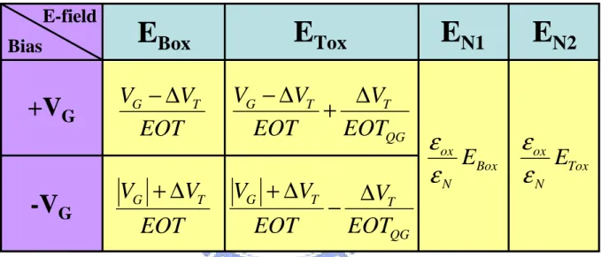
page Table 2.1 E-fields of ONO films under both positive and negative gate biases for
arbitrary charge location... 47 Table 8.1 Theoretical modeling flow chart for transient gate current modeling by
assuming fully capturing... 187
Table F.1 MFN fitting parameters of SoNOS, SONoS, BE-SONOS, top
LIST OF FIGURES
page
Fig. 1.1 Summary of semiconductor memory………... 10
Fig. 1.2 Two classes of non-volatile semiconductor memory: (a) floating gate
(FG) memory; (b) charge-trapping (CT) memory.……….. 11
Fig. 1.3 D. Kahng and S. M. Sze proposed first non-volatile memory device in 1967. Program and erase are performed by direct tunneling (DT) of
electrons through the thin oxide I1.……….… 12
Fig. 1.4 Wegener et al. proposed MNOS memory in 1967. This device is programmed by electrons tunneling from the Si conduction band to nitride trapping centers and erased by holes tunneling from the Si
valence band to the nitride trapping centers.……….……….. 13
Fig. 1.5 FAMOS (Floating gate Avalanche injection MOS). Program is performed by injection of high energetic electrons created in the drain avalanche plasma while erase is possible by UV or X-ray radiation.….… 14 Fig. 1.6 SAMOS (Stacked gate Avalanche injection MOS) memory. Its program
speed is higher than FAMOS memory due to the additional external gate. Erase can be achieved by field emission through the top dielectric....…… 15 Fig. 1.7 Evolution of SONOS-type memory. (a) P-channel MNOS. (b) N-channel
SNOS. (c) N-channel SONOS.……… 16
Fig. 1.8 (a) Program (+10V) operation and (b) erase (–10V) operation of SONOS. During programming, the channel electrons inject into nitride. On the other hand, during erasing the channel holes inject into nitride to
compensate for trapped electrons.………... 17
Fig. 1.9 Simulation of hole tunneling current density (Jh) to tunnel oxide electric
field (Eox) with various thickness schemes. To enhance required erase
current density under reasonable erase field, a very thin tunnel oxide such as 25Å is necessary. However, a conflict to data retention
performance will be suffered.……….. 18
Fig. 1.10 BE-SONOS (band-gap engineered SONOS) memory. A composite ONO
tunneling barrier could provide high erase speed as well as excellent data
retention.……….. 19
Fig. 1.11 Band-offset effect by using an ONO barrier as tunneling dielectric in BE-SONOS memory. (a) At high e-field, the band offset happens so that the holes directly tunnel through the O1. (b) At low e-field (retention
state), both electron de-trapping and hole external tunneling are
prohibited by the total O1/N1/O2 barrier stack………...……… 20
Fig. 2.1 (a) Storage principle of non-volatile memory devices can be simplified as the charges (QT) are trapped in the gate insulator of a MOSFET. (b)
Influence of trapped charges in the gate insulator on the threshold
voltage (VT) shift of a MOSFET.……….... 42
Fig. 2.2 ONO energy band diagram of SONOS memory under zero bias………… 43
Fig. 2.3 (a) ONO energy band diagram of SONOS memory under positive gate bias. (b) The trapped electrons at nitride/B.O. interface will cause
decreased EBox but increased EN..…...…….……….………... 44
Fig. 2.4 ONO energy band diagram of SONOS memory for the trapped electrons at the center of nitride. The nitride is divided into two equal parts. The bottom nitride e-field is EN1 while the top nitride e-field is EN2.………... 45
Fig. 2.5 ONO energy band diagram of SONOS memory under (a) positive gate bias, and (b) negative gate bias for the general case: the trapped charges
locate at x from B.O./nitride interface.……… 46
Fig. 2.6 Energy band diagrams of SONOS-type devices under (a) positive and (b) negative gate biases. The main conduction mechanisms are also indicated. Solid circles represent electrons, and hollow circles represent
holes [2.5].……….………... 48
Fig. 2.7 Energy band of diagrams of (a-c) electron injection and (d-f) hole injeciotn from Si-sub to nitride under various gate biases. (a,d) Fowler–Nordheim (FN) tunneling. (b,e) Direct tunneling (DT). (c,f) Modified Fowler–Nordheim (MFN) tunneling. Φ1 and Φ2 are the oxide
and nitride barrier heights for electron, respectively. Φ1 and Φ2 are the
oxide and nitride barrier heights for hole, respectively.……….…. 49 Fig. 2.8 Schematic diagrams of CHEI in (a) NMOSFET and (b) PMOSFET
[2.7].……….…… 50
Fig. 2.9 Schematic diagrams of BBHC injection in (a) NMOSFET and (b)
PMOSFET [2.7].……….………. 51
Fig. 2.10 Schematic diagram of retention charge loss mechanisms of SONOS devices: trap-to-band tunneling (TB), trap-to-trap tunneling (T-T), band-to-trap tunneling (B-T), thermal excitation (TE) and Poole–Frenkel
emission (PF) [2.12]..……….………. 52
Fig. 2.11 (a) Standard charge pumping (CP) measurement setup. (b) VT profile in a
CHE programmed charge trapping memory. (c) and (d) are measured Icp
curves vs. Vh and Vb before and after CHE program using CVb and CVh,
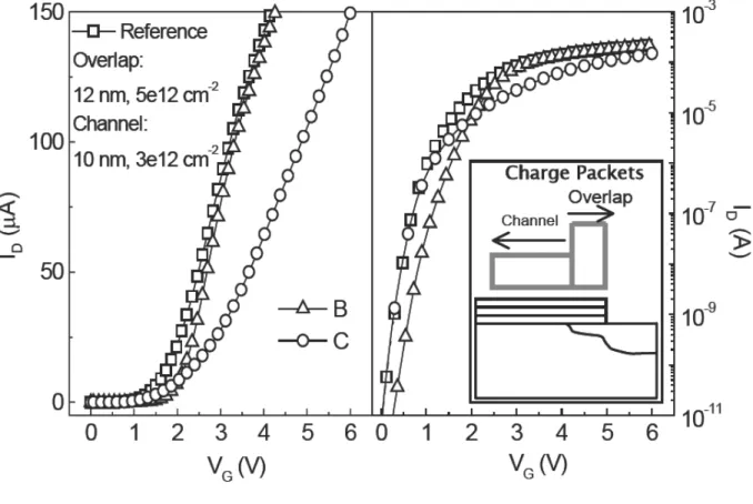
Fig. 2.12 Simulated ID-VG with different amount of charge placed in rectangular
packets. Increasing channel charge spread (curve B) affects S.S. and VT.
Increasing overlap charge magnitude (curve C) degrades linear slope and
VT but does not affect S.S [2.23]..……….……….. 54
Fig. 2.13 Maximum memory window ∆VFBmax as a function of γ. γ means the
fraction of the nitride converted by oxidation. Initial nitride thickness is
(a) 45.7Å, (b) 76Å, and (c) 59.2Å [2.27].……….…………... 55
Fig. 2.14 (a) Three trap sites in the MONOS structure. The trap distributions in these three regions were uniform. Analytical results of electron trap
density in (b) MNOS and (c) MONOS structures [2.28]..………... 56
Fig. 2.15 A block diagram of the automated data-acquisition system for the linear voltage ramp technique with charge separation [2.31]...………... 57 Fig. 2.16 Energy band diagrams and the corresponding currents at various points
in the voltage sweep on a MONOS transistor [2.31].……….. 58
Fig. 2.17 (a) Measurement setup for carrier separation and charge-centroid extraction. (b) Waveforms for the P/E pulses showing the three-level shape used to obtain a null contribution to the overall current integral of
the displacement charge in the semiconductor [2.33]………. 59
Fig. 2.18 Transient analysis of J vs. ETox for SONOS devices with N+-poly gate
and different T.O. (a) Thermal oxidation T.O. and (b) HTO T.O [2.35]..… 60 Fig. 3.1 Schematic diagrams that illustrate the gate-sensing (GS) and channel-
sensing (CS) transient analysis method.………...…. 74
Fig. 3.2 (a) Bulk trap model: definition of the sheet charge density (Q) and vertical location (x). (b) A two-region approximation model: Q1 and Q2
are the charges inside the bottom and top portions of nitride, respectively 75 Fig. 3.3 CV curves of SONOS (ONO=54/70/90Å) during +FN programming (a)
CS capacitor (b) GS capacitor.………...………...….……. 76
Fig. 3.4 Comparison of the VFB shifts of SONOS (ONO=54/70/90Å) during +FN
programming. “GS” indicates the gate-sensing results, and “CS”
indicates the channel-sensing results.……….. 77
Fig. 3.5 (a) Q-t and (b) x-t of SONOS (ONO=54/70/90Å) transformed from Fig. 3.4 by using Eqs. (3.3) and (3.4). (c) x-Q transformed from Q-t and x-t… 78 Fig. 3.6 J vs. EBox curves of GS capacitor by assuming different charge vertical
locations. (a) Charges are at T.O./nitride interface. (b) Charges are at B.O./nitride interface. (c) Charges are at center of nitride.………. 79 Fig. 3.7 Comparison of (a) ∆VFB,CS-t and (b) ∆VFB,GS-t with the theoretically
calculated results by assuming different charge vertical locations.………. 80 Fig. 3.8 x-t and Q-t plots for different thickness measurement errors. (a) and (b)
show the B.O. thickness variation. (c) and (d) show the nitride thickness variation. (e) and (f) show the T.O. thickness variation.………... 81 Fig. 3.9 (a) ∆VFB,CS-t and (b) ∆VFB,GS-t for ±2% and ±5% variation in B.O.
thickness during +FN programming.………... 82
Fig. 3.10 x-t and Q-t plots transformed from Fig. 3.9. (a) and (b) show CS capacitor has ±2% and ±5% variation in B.O. thickness from 54Å. (c) and (d) show GS capacitor has ±2% and ±5% variation in B.O. thickness
from 54Å.………. 83
Fig. 3.11 Comparison of GS capacitors (BE-SONOS, ONONO = 13/20/25/60/ 60Å) with different poly gate doping concentrations. (a) CV curves. (b)
∆VFB,GS during +FN programming. (c) ∆VFB,GS during –FN erasing. The
∆VFB,GS is insensitive to poly gate doping concentrations.……….. 84
Fig. 3.12 Comparison of CS capacitors (BE-SONOS, ONONO = 13/20/25/70/ 90Å) with different well doping concentrations. (a) CV curves. (b)
∆VFB,CS during +FN programming. (c) ∆VFB,CS during –FN erasing. The
∆VFB,CS is insensitive to well doping concentrations..………. 85
Fig. 3.13 Comparison of GS capacitors (BE-SONOS, ONONO = 13/20/25/70/ 90Å) with different well doping concentrations. (a) CV curves. (b)
∆VFB,GS during +FN programming. (c) ∆VFB,GS during –FN erasing. The
more heavily doped well has slower program speed but keeps the same
erase speed.……….. 86
Fig. 4.1 Calculated x-Q plots for various SONOS-type devices. (a) SONOS (54/70/90Å), (b) SONOS (70/95/75Å), (c) BE-SONOS (15/20/25/70/90 Å), and (d) SONOS (20/70/90Å). The final charge centroids of all
devices are close to the center of nitride.……… 97
Fig. 4.2 x-Q plot (electron centroid evolution) of SNOS (NO = 70/90Å)
calculated from ∆VFB-t (inset).……….………... 98
Fig. 4.3 x-Q plot (electron centroid evolution) of SNOS (NO = 60/75Å) calculated from ∆VFB-t (inset). Compared with NO = 70/90Å, the
electron centroid is closer to the nitride/T.O. interface.………... 99 Fig. 4.4 (a) Measured ∆VFB of SONS (ON = 54/70Å) during +FN programming.
The GS capacitor initially shows hole injection (∆VFB < 0), and then
shows electron injection after longer time programming (∆VFB > 0). On
the other hand, CS capacitor shows only electron injection (∆VFB > 0).
Calculated (b) Q-t and (c) x-t from (a). The results show that initially SONS has net hole injection, but eventually becomes electron trapping. On the other hand, the charge centroid initially locates at the nitride
Fig. 4.5 Two-region charges (Q1-t, Q2-t) of (a) SONS (ON = 54/70Å) calculated
from Fig. 4.4(a) and (b) SNS (N = 70Å) calculated from ∆VFB-t (inset).
The hole trapping in Q2 is caused by the hole injection from poly gate
because the nitride has a small hole barrier height (~ 2eV). This hole trap signal can only be detected by the GS capacitor because holes are located
near the gate..…...……….………... 101
Fig. 4.6 Comparison of the theoretical and experimental injected electron densities (Q-t) for various SONOS. (a) ONO = 54/70/90Å, (b) ONO = 70/70/90Å, (c) ONO = 90/70/ 90Å, and (d) ONO = 70/95/75Å. All samples show excellent fit with theory, and the fitting parameters are very close. This suggests that the devices with N≧70Å have high
enough capture efficiency...……….……… 102
Fig. 4.7 Comparisons of the theoretical and experimental injected electron densities (Q-t) for various SONOS with thinner nitride thickness ((a) ONO = 54/35/90Å and (b) ONO = 54/20/90Å) and injected electron densities (Q1-t) for (c) SONS (ON = 54/70Å) and (d) SNS (N = 133Å).
We used 3.1eV oxide barrier height, 2.2eV nitride barrier height, and 0.45m0 effective mass for fitting. The results indicate the capture
efficiency drops significantly for N below 35Å and becomes negligible when N is only 20Å. Moreover, the nitride without T.O. has very low “apparent” capture efficiency due to hole injection from gate.……..……. 103 Fig. 4.8 (a) Comparison of the theoretical (Qthe) and experimental (Qmea) injected
electron densities for various trap-layer engineered devices. SiN (70Å), SiON (70Å), SiN+SiON (35+35Å), SiON+SiN (35+35Å), SiN (35Å), and NON (20+25+20Å). The ideal fully-capturing line is also drawn. (b) Comparison of ISPP for various trap-layer engineered devices. The ideal
ISPP slope for fully-capturing is 1..………. 104
Fig. 5.1 ∆VFB during (a) programming by +20V and (b) erasing by –VG stress.
Calculated Q-x plots for (c) +FN program and (d) –VG stress. For
electron injection (+FN), the electron centroid gradually migrates toward the center of nitride. After –VG stressing, the electron density decreases
while the electron centroid moves upward. It indicates that electrons
mainly de-trap from the bottom portion of nitride..……… 115
Fig. 5.2 X-Q plots of various SONOS devices (B.O. = 54Å, 70Å, and 90Å) during –VG stressing. Thicker B.O. shows less x-variation at first. At
long-term stress, the x variations are becoming identical for all samples... 116 Fig. 5.3 (a) program and (b) erase characteristics of SONOS device with an
(b) –FN erase. During –FN erasing injected holes first recombine with the bottom electrons and then gradually move upward, thus causing the
upward motion of the charge centroid..………..………... 117
Fig. 5.4 (a) –FN hole injection characteristics of BE-SONOS (13/20/25/70/90Å). (b) Q-t and (c) x-t/x-Q plots. The x-Q plot is transformed by Q-t and x-t plots. The injected holes first recombine with the bottom electrons..……. 118 Fig. 5.5 (a) Qh-t and (b) xh-Qh plots of BE-SONOS (13/20/25/70/90Å)
during –FN erasing by using Eqs. (E-5, E-6). Hole centroid also starts at the bottom interface. After longer injection, it gradually migrates upward. However, its centroid is much lower than that of trapped
electrons..………..……….……..……… 119
Fig. 5.6 (a) 10K P/E cycling endurance of BE-SONOS (15/20/25/70/90Å). (b) Extracted Q and x. After +FN programming, the Q (electrons) increases, and x is close to the nitride center. After –FN hole injection, Q (still more electrons since Q > 0) decreases, and x shifts higher..……… 120 Fig. 5.7 (a) 200oC (b) 250oC baking retention of SONOS (54/70/90Å) and
BE-SONOS (15/20/25/70/90Å). The device is first programmed by +20V 0.26sec before high-temperature baking. (c) Q-t and (d) x-t/x-Q plots. x first moves lower within 1-day baking, and then shifts upward after longer time baking. X-Q plots for different baking temperatures are
similar..………..……….……..………... 121
Fig. 5.8 (a) 250oC post-cycling baking characteristics of BE-SONOS (15/20/25/ 70/90Å). The devices are programmed by +19V before baking. (b) Q-t and (c) x-t/x-Q plots. The x-Q plot is transformed from Q-t and x-t plots. P/E cycling stress only causes more initial charge loss, but it has no
effect on the long-term retention……..……….……..…… 122
Fig. 5.9 (a) 250oC baking retention of SONOS (ONO = 70/95/75Å). The device is programmed by +20V 0.26sec or +21V 0.26sec before baking. Within 1 day baking, CS device shows obvious VFB gain while GS device shows
VFB loss. (b) Q-t and (c) x-t plots. During 1 day baking, Q is almost
unchanged while x is significantly decreased. This indicates that electron moves from the top portion toward the bottom portion..……..…………... 123 Fig. 5.10 (a) 150oC baking retention of SONOS (ONO = 70/95/75Å). The device
is programmed by +20V 0.26sec or +21V 0.26sec before baking. There is no significant VFB gain or VFB loss. (b) Q-t and (c) x-t plots. The
amount of change in x is much smaller than that in Fig. 5.9(c)..………… 124 Fig. 5.11 (a) Q-t and (b) x-t plots of SONOS (ONO = 70/95/75Å) during ±5V gate
Fig. 6.1 (a) Top BE-SONOS with ONO barrier at the top and (b) SONoS with a thin top oxide. Both program and erase are by gate injection.……… 136 Fig. 6.2 Comparison of GS capacitors (Top BE-SONOS, ONONO = 94/70/30/20/
12Å) with different poly gate doping concentrations. (a) CV curves. (b)
∆VFB,GS during –FN programming. (c) ∆VFB,GS during +FN erasing. The
∆VFB,GS is insensitive to poly gate doping concentrations.……….. 137
Fig. 6.3 Comparison of CS capacitors (Top BE-SONOS, ONONO = 94/70/30/20/ 12Å) with different poly gate doping concentrations. (a) CV curves. (b)
∆VFB,CS during –FN programming. (c) ∆VFB,CS during +FN erasing. The
device with more lightly doped poly gate has larger ∆VFB,CS.……… 138
Fig. 6.4 (a) –FN electron gate injection characteristics of SONOS (54/70/90Å). CS capacitor has larger ∆VFB because its T.O. is thicker than B.O. (b)
Q-t and (c) x-t/x-Q plots. The x-Q plot is transformed by Q-t and x-t plots. The final mean vertical location is close to nitride center (~ 35Å)... 139 Fig. 6.5 Calculated x-Q plots for various SONOS devices. (a) 54/70/90Å, (b)
54/80/70Å, (c) 54/75/45Å, and (d) 54/80/25Å. For all samples, the final mean vertical locations are close to nitride center.………..… 140 Fig. 6.6 Calculated x-Q plots for various top BE-SONOS devices. (a)
54/70/25/20/15Å and (b) 54/70/20/20/15Å. For all samples, the final mean vertical locations are close to nitride center.………...……... 141 Fig. 6.7 Comparisons of J vs. ETox curves of SONOS (54/70/90Å) by assuming
different charge vertical locations. The charge centroid is more likely
located near the nitride center (Case 3 in (c)).………….……… 142
Fig. 6.8 (a) –FN electron injection characteristics of SONS (ON=54/70Å). (b) Calculated x-Q plot. The final mean vertical location is inside nitride instead of accumulating at the nitride/B.O. interface. This suggests that the major charge trapping is not at the O/N interface.………. 143 Fig. 6.9 (a) Q-t and (b) X-t/x-Q plots of top BE-SONOS (54/70/20/20/15Å)
during +FN erasing. The devices are first programmed by –17V 0.26sec by electron gate injection, and then erased by various +FN voltages. The injected holes first recombine with the top electrons resulting in the
downward motion of the charge centroid.……….……….. 144
Fig. 6.10 Calculated Q-t results for (a) SNOS (70/70Å) and (b) SNS (120Å) by using two-region approximation method. Q1 and Q2 indicate the charges
inside the bottom and top portions of nitride, respectively. The polarities
of Q1 and Q2 are also shown.……….….. 145
Fig. 6.11 Extracted (a) Q-t and (b) x-t plots during 10K P/E cycling endurance of SONoS (54/80/25Å). The program and erase conditions are –15V 4msec
and +10V 0.3sec, respectively. At the initial few P/E cycles, the Q and x are slightly varied, but then soon become very stable after many P/E
cycling.……….……….……... 146
Fig. 6.12 (a) Comparison of 250oC retention characteristics of fresh and post-10K cycling devices. (b) Extracted x-Q curves. The devices are programmed at –15V 0.26sec before baking. As the total charge (Q) decreases with time due to charge loss, the x of fresh device stays almost constant, but
the x of post-10K cycling device shifts lower.………..…….. 147
Fig. 6.13 Comparisons of the experimental and theoretical Q-t for (a) 54/70/90Å and (b) 54/80/70Å at various –FN program voltages. The experimental Q-t is well correlated with the theoretical results.………... 148 Fig. 7.1 (a) Program and (b) erase characteristics of SoNOS (20/70/90Å).………. 159 Fig. 7.2 (a) X-t and (b) Q-t of SoNOS (20/70/90Å) during programming
transformed from Fig. 7.1(a). X-t shows that electron centroid migrates from the bottom interface toward the center of nitride. On the other hand, Q-t has a similar shape as ∆VFB-t. (c) X-t and (d) Q-t of SoNOS during
erasing transformed from Fig. 7.1(b). The charge centroid (remained electron) moves upward toward the top interface, and the electron
density decreases.……….……... 160
Fig. 7.3 J vs. Eox of SoNOS (20/70/90Å) during erasing by using Eqs. (7-1) and
(7-2). Different erase voltages follow the same trend, and they can be
well fitted by MFN equation.………... 161
Fig. 7.4 (a) Program and (b) erase characteristics of SONoS. (c) X-Q during erasing transformed from (b). The charge centroid moves downward toward the bottom interface as electron density decreases. (d) J vs. Eox during erasing by using Eqs. (7-1) and (7-3). Different erasing voltages follow the same trend, and they can be well fitted by MFN equation..…... 162 Fig. 7.5 (a) J vs. Eox curves of BE-SONOS (13/20/25/70/90Å). (b) Comparison of
J vs. Eox curves for BE-SONOS with various N2/O3 thickness. All J-E
curves overlap in one single cluster. Therefore, we can know that the hole injection is independent of N2/O3 compositions. The J-E curves can
be well fitted by MFN model.……….. 163
Fig. 7.6 J vs. Eox of top BE-SONOS capacitors during erasing by using Eqs. (7-1)
and (7-3). Different erase voltages follow the same trend. Both samples
can be well fitted by MFN model.………... 164
Fig. 7.7 (a) Erase characteristics and (b) J vs. Eox of SONOS (26/70/90Å). The
erase speed is much smaller than SoNOS (Fig. 7.1(b)). At initial erasing, the dominant erase mechanism is electron de-trapping while hole
tunneling dominates after long erasing time, and the J-E curves follow
MFN equation.………. 165
Fig. 7.8 (a) Erase characteristics of SONOS (54/70/90Å). The erase speed is much slower than SONOS with thinner B.O. (b) J vs. Eox of 54/70/90Å,
70/70/90Å, and 90/70/90Å. The J-E curves are very scattered for different B.O. thickness and erase conditions. Electron de-trapping
contributes to charge loss.……… 166
Fig. 7.9 J vs. Eox curves of (a) SoNOS (20/70/90Å), (b) BE-SONOS (13/20/25/70
/90Å), (c) SONoS (54/80/25Å), and top BE-SONOS (54/70/25/20/15Å). J-E curves are simply identical after several refill times. Hole-tunneling
injection can be repeated continuously.…………..………. 167
Fig. 7.10 J vs. Eox curves of SONOS (26/70/90Å). The J slightly decreases during
refill. Some electron de-trapping occurs during erasing. Finally, the
erasing current J mainly comes from hole tunneling.……….. 168
Fig. 7.11 (a) Refill characteristics of SONOS (54/70/90Å). The ∆VFB decreases
during refill. (b) X-t and (c) Q-t during refill transformed (a). During –VG stressing the x is slightly increased, but the Q is decreased.
After refill sequence x-t plot is repeated, but charge loss is significantly decreased. It means that the refill characteristic does not come from the charge vertical profile modulation, but comes from energy spectrum shift. (d) J vs. Eox curves. The J decreases during refill. Electron
de-trapping occurs during erasing, and the energy level of injected electrons changes from shallow to deep, which results in smaller J..……. 169 Fig. 7.12 (a) Charge loss vs. refill times of experimental data and mathematical
model fitting. The experimental data can be well fitted by mathematical model. (b) Simulated results of energy spectrum. Each refill sequence shifts the trapping energy higher (blue shift) and the distribution tighter,
and it finally saturates.………. 170
Fig. 8.1 Pulse-IV setup for (a) transistor and (b) capacitor measurements. For transistor, pulses are applied to the gate and drain while source is connected to a current-voltage amplifier. Both gate pulse and source current can be monitored by oscilloscope. For capacitor, pulse is only applied to gate, and source/drain/body are connected together to measure
the total tunneling current..……….. 181
Fig. 8.2 Transient tunneling current of SOS (25Å) capacitor under various (a) gate voltages and (b) pulse widths. The Itotal stays constant, and there is
no transient relaxation for a pure gate oxide. This indicates that our
Fig. 8.3 Transient tunneling current of SNS (133Å) capacitor under various (a) gate voltages and (b) pulse widths. The Itotal drops during the VG pulse.
This can be explained by the net electron trapping that results in decreased electron tunneling current. In (b), longer VG pulse does not
change the Itotal relaxation behavior..………... 183
Fig. 8.4 Transient tunneling current of SONS (54/114Å) capacitor under various (a) gate voltages and (b) pulse widths. The Itotal rises during the VG pulse.
This indicates that there is some hole trapping (coming from gate injection) that increases the substrate electron tunneling.………... 184 Fig. 8.5 (a) Area and (b) temperature dependence of SNS (133Å) and SONS
(54/114Å). The Itotal in (a) is normalized to area. The transient behaviors
are independent of area and temperature.……… 185
Fig. 8.6 (a) CV curves of SONOS (54/70/90Å) capacitor before and after programming. (b) The transient tunneling current during +FN programming shows a large Itotal initially but decreases afterwards.
Moreover, the measured Itotal can be well fitted with our model..………... 186
Fig. 8.7 Comparison of dual-sweep DC-IV for SONS with standard and silicon-rich nitride-trapping layer. (a) N-channel transistors. (b) P-channel transistors. Gate voltage sweeps from –5V to +5V, and then +5V to –5V for n-channel, and it sweeps reversely for p-channel. The hysteresis direction is also indicated. The inset is the typical
cross-sectional view of SONS device.………. 188
Fig. 8.8 (a) Designed VG and VD pulses for P/E and read. Reading (VG = –2V and
VD = –1V) is performed immediately after P/E. (b) Typical measured
drain current response during a P/E test. Large current difference (~
10µA) is obtained after programming/erasing...……….. 189
Fig. 8.9 Program and erase transient behavior of SONS ((a) and (d)), SONoS ((b) and (e)), and SoNOS ((c) and (f)) p-channel transistors. SONS shows the fastest program and erase speeds. SoNOS uses inverse polarity (–VG for
the program, and +VG for the erase) because it is channel-injection mode. 190
Fig. 8.10 (a) Endurance characteristics of SONS, SONoS, and SoNOS. SONS shows the best memory window. (b) Endurance characteristics of SONS device under different bias voltages and P/E time. At +/–6V operation,
more than 1010 P/E cycling is achieved.……….…. 191
Fig. 8.11 (a)-(c) Field dependence and (d)-(f) temperature dependence of retention characteristics of SONS, SONoS, and SoNOS. SONS and SONoS are P/E by +/–8V 50µs while SoNOS is P/E by –/+8V 50µs before retention test. Different external gate voltages (waiting voltage) are applied for
field-dependence retention test while different in-situ baking temperatures are applied for temperature-dependence retention test. The retention characteristics of all devices are sensitive to the waiting
voltages, but not on the storage temperatures.………. 192
Fig. D.1 Curve fitting of the experimental x-Q plot (Fig. 3.5). Hyperbolic function is used to fit the experimental data. This fitting x-Q curve is used to theoretically calculate VFB-t for both CS and GS capacitors..………. 216
CHAPTER ONE
INTRODUCTION
OUTLINE
1.1 Non-volatile Memory Review………..
1.1.1 Historical Review………..……….….….….………. 1.1.2 Evolution of SONOS Memory……….….…… 1.1.3 Value and Restrictions of SONOS Memory……….….…
1.2 Motivation and Objectives of Research……… 1.3 Dissertation Organization……… 2 2 4 5 7 7
1.1 Non-volatile Memory Review
Generally speaking, semiconductor memory can be split into two main categories: volatile and non-volatile, as illustrated in Fig. 1.1.Volatile memory loses its data as soon as the power is turned off while non-volatile memory does not lose its data even when the power is turned off. Due to this permanent storage characteristic, non-volatile memory has been widely used for data storage in electronic products, and there have been many related studies. In this chapter, we will focus on the non-volatile memory.
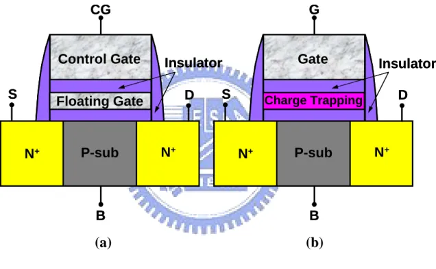
According to the storage materials, non-volatile memory can be divided into two classes. For the first class, the injected charges are stored in a conducting or semiconducting material which is completely surrounded by insulators, as shown in Fig. 1.2(a). Since the storage material acts as a completely electrically isolated gate, we call this kind of memory as floating gate (FG) memory [1.1-1.2].On the other hand, for the second class, the injected charges are stored in “discrete” trapping centers of a dielectric material instead of conducting or semiconducting material, as illustrated in Fig. 1.2 (b). Due to this charge trapping characteristic, we call this kind of memory as charge-trapping (CT) memory [1.3-1.4].
In this section, we will first review the history of non-volatile memory and then introduce the evolution and restrictions of SONOS memory.
1.1.1 Historical Review
The first non-volatile memory device was proposed by D. Kahng and S. M. Sze in 1967 [1.5], and the possibility of non-volatility in MOS-type device was also first recognized. Figure 1.3 illustrates the proposed non-volatile memory. They used layered structure (from bottom to top: thin oxide Il, floating metal M1, thick oxide I2, and metal gate M2) to replaced
the gate dielectric of conventional MOSFET. Since the metal-insulator-metal-insulator- semiconductor structure, it was calledMIMIS memory.
high e-field in the I1 could provide sufficient electron tunneling (direct tunneling, DT), and
then these injected electrons are "captured" in Ml since the thick I2 could block injected
electrons from discharging to M2. When the gate voltage is removed, the electron
out-tunneling is blocked by I1 and I2, therefore, these captured electrons will stay in floating
gate. On the other hand, using the same tunneling mechanism (DT), the captured electrons can be removed from the floating gate by applying a negative voltage to M2 (erase operation).
However, the operation (DT) of MIMIS memory needs a very thin oxide (< 2.5nm) [1.6-1.7]. It is difficult to fabricate such thin oxide without any defect. Moreover, any pinhole in I1 will leak all the stored charges in M1 due to its conductive property. Due to these issues,
this MIMIS memory could not be realized at that time. However, MIMIS memory still was a pioneer in the non-volatile memory industry.
There are two possible solutions to solve the issues of MIMIS memory. One is replacing the M1 by a charge trapping dielectric, and anther is increasing the thickness of I1.
For the first solution, metal-nitride-oxide-semiconductor (MNOS) memory was introduced in 1967 by Wegener et al [1.8], as illustrated in Fig. 1.4.In the MNOS, the M1 and
I2 in MIMIS are replaced by nitride which has “discrete” trapping centers, therefore, the
pinhole in I1 will not cause trapped charges to leak out. This device is programmed by
applying a high positive voltage to the gate, so electrons tunnel from the Si conduction band to the nitride and are then trapped into the trapping centers. On the other hand, erase is achieved by applying a high negative voltage to the gate, so that holes tunnel from the Si valence band and are then trapped into the trapping centers.
For the second solution, floating gate avalanche injection MOS (FAMOS) was first proposed by Frohman-Bentchkowsky in 1971, as illustrated in Fig. 1.5 [1.9-1.11]. Since the tunnel oxide of FAMOS memory is thicker (~ 100nm), DT is excluded. Therefore, special program and erase are needed. Program is performed by biasing the drain junction to avalanche breakdown (V > 30V), such that the electrons in the avalanche plasma can inject
from the drain region into the floating gate. On the other hand, erase is carried out by ultraviolet (UV) or X-ray. FAMOS memory finally evolved into electrically programmable read-only memory (EPROM).
However, FAMOS memory had some drawbacks such as inefficient program and inconvenient erase, and that could be improved by several methods. For example, in stacked gate avalanche injection MOS (SAMOS) memory [1.12-1.13], an external gate is added, as illustrated in Fig. 1.6. The external gate can further improve the programming efficiency. Moreover, electrical erase also became possible by field emission through the top dielectric. Therefore, electrically-erasable programmable read-only memory (EEPROM) products became feasible.
1.1.2 Evolution of SONOS Memory
The first CT memory based on nitride trapping layer was proposed for more than 40 years. The charges (electrons/holes) are injected from channel into nitride by tunneling through an ultra-thin oxide (typically 1.5 to 3nm). Typically, the trapped charges can be maintained in nitride for at least 10 years if the nitride can be isolated perfectly.
The first product level nitride based CT memory was available in 1975 by P-channel MNOS [1.14], as illustrated in Fig. 1.7(a). It consists of aluminum (Al) gate electrode, 45nm nitride charge trapping layer, and 2nm tunnel oxide. However, this memory had several issues. The first one is the high operation voltage (25-30V) because of its thick gate stack. The second one is the large standby current since the p-channel device is in depletion mode when there are electrons stored in the nitride. Moreover, the most important one is the metal gate which is the terribly pollutant in IC fabrication. Therefore, finding other material to replace metal gate was necessary.
The most important breakthrough for CT memory was the development of the Si-gate n-channel silicon-nitride-oxide semiconductor (SNOS) in 1980 [1.15], as illustrated in Fig.
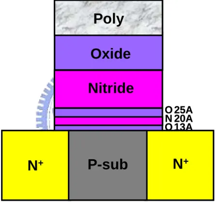
1.7(b). Scaling down the nitride thickness (25nm), the operation voltage can be reduced to 14-18V. However, if we further scale down the nitride thickness, the channel injected charges may directly tunnel out to gate, or the trapped charges may de-trap to gate. Moreover, the gate injected charges may also affect the stored charges in nitride.
These issues can be eliminated d by providing an oxide on top of nitride, as shown in Fig. 1.7(c), and we called it as SONOS (silicon-oxide-nitride-oxide-semiconductor) memory [1.3,1.16]. Due to the insertion of top oxide, the nitride thickness can be further reduced to 5nm, and the operation voltage can be around 10V. Figure 1.8 shows the program/erase operations of SONOS memory. Under +10V (VG = +10V, VS = VD = VB = 0V) programming,
the channel electrons can inject into nitride by DT, and are then trapped into trapping centers. On the other hand, under –10V (VG = –10V, VS = VD = VB = 0V), the channel holes can inject
into nitride to compensate for trapped electrons.
1.1.3 Value and Restrictions of SONOS Memory
The rapidly growing market share of memories has brought about competitive development of memory technologies. Among different types of memories, Flash memory has become extremely attractive due to its significant advantages such as non-volatility, repetitive electrical program/erase capability, high density, low cost, low power consumption, high speed, high endurance, and long data retention [1.17-1.19]. The most particular feature of Flash memory is that the content of the whole chip can be cleared in one step, so called “Flash” memory.
Conventional Flash memory using floating gate (FG) device has become the major product in non-volatile memory since 1990s, however, the high voltage operation and the scaling limitation have prompted the search of new Flash memory design. The most promising structure is SONOS because of the good scalability, simple process, and low voltage operation [1.20-1.22]. Since the nitride has “discrete” charge-trapping characteristic,
the insulating oxide layers can be further scaled down without pinhole effect, and the physically 2-bits-per-cell operation is allowed (NROM concept) [1.23-1.25]. Moreover, it also offers immunity to stress-induced leakage current (SILC) and provides good few-electron storage capability. On the other hand, SONOS is also a candidate for embedded memory applications because its processes are compatible with conventional CMOS technology, except for the formation of the oxide-nitride-oxide (ONO) dielectric stack.
However, the thin tunnel oxide in SONOS still causes some problems due to the considerable direct tunneling leakage under low e-field. This can be explained by the simulated hole tunneling current density (Jh) vs. tunnel oxide e-field (Eox) curves with various
oxide thickness, as shown in Fig. 1.9. To enhance required erase current density (> 10-4A/cm2) under reasonable erase field (~ 11MV/cm), a very thin tunnel oxide (< 25Å) is necessary. However, a conflict to data retention performance will be suffered because at low e-field the direct tunneling leakage can not be avoided. This means that there is no single tunnel oxide thickness that can satisfy both fast erase speed and good data retention.
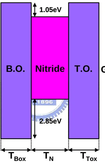
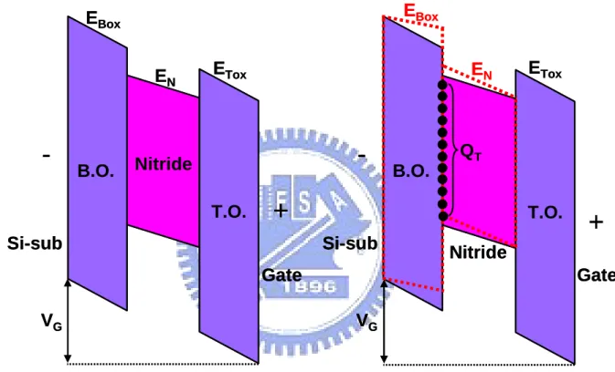
Recently, a novel band-gap engineered SONOS (BE-SONOS) memory was proposed [1.26] to provide high erase speed as well as excellent data retention. Figure 1.10 shows that in BE-SONOS a composite ONO tunneling barrier is applied to replace the traditional tunnel oxide in SONOS. This ONO barrier has different functions for program/erase and data retention, as shown in Fig. 1.11. Under high e-field (Fig. 1.11(a)), the band offset happens so that the barrier height of N1 and O2 are almost screened, then the holes can directly tunnel through the O1 (13Å). On the other hand, at low e- field retention state (Fig. 1.11(b)), both electron de-trapping and hole external tunneling can be completely suppressed by the total barrier stack (O1+N1+O2). Based on such band-offset effect, the thickness of ONO barrier becomes variable and adjustable for the required high-field hole tunneling current and low-field retention criteria, so that the device performance can be further optimized. Therefore, BE-SONOS is promising for next generation non-volatile memory.
1.2 Motivation and Objectives of Research
Although SONOS memory has turned into products, the understanding of trapped charge behaviors is still limited. Since the trapped charge behaviors govern the device performance and reliability of SONOS memory, characterizations of charge-trapping behaviors are the crucial needs to optimize the device performances.
In this dissertation, we proposed several new techniques to extensively investigate the charge trapping behaviors of various SONOS-type devices, including SONOS, BE-SONOS, SONS (SONOS without top oxide), SNOS (SONOS without bottom oxide), SNS (SONOS without top and bottom oxides), and Top BE-SONOS (an upside-down BE-SONOS). We wish to provide in-depth physical understanding of trapped charge behaviors.
1.3 Dissertation Organization
The organization of this dissertation is briefly described below.
Chapter 2 introduces the basic of SONOS-type memory. The basic operating principle and models used in this dissertation are introduced. The main charge transport mechanisms for device operations are also discussed in detail. Moreover, we summarize some papers which investigated the trapped charge locations for both lateral and vertical directions.
In chapter 3, the principle of our novel gate-sensing and channel-sensing (GSCS) method is discussed in detail, including the theoretical equations, sample preparation, basic device characteristics, and method demonstration. We also compare GSCS method with other previous methods for a systematic understanding. Therefore, the results obtained by our method can be double-confirmed, and the advantages of our method can be fully understood. Moreover, several factors that affect the accuracy of our method are also analyzed.
Chapter 4 illustrates the applications of GSCS method on the charge centroids as well as the capture efficiency of various SONOS devices. Using bulk trap model to compare SONOS,
SONS, and SNOS, we can clearly verify that electrons are mainly distributed inside the bulk nitride or the interfaces between oxide and nitride. On the other hand, using two-region approximation model, we can successfully monitor the channel injected charges as well as the gate injected charges for SONS and SNS. Based on the theoretical Q-t model, we can further fit our data with that extracted by GSCS method, and further to obtain the capture efficiency of different nitride layers.
Chapter 5 illustrates the applications of GSCS method on the intra-nitride transport behaviors and the reliability of various SONOS devices. For the first time, we can directly investigate the intra-nitride charge transport behaviors of SONOS-type devices during ±FN injection, FN cycling, and high temperature baking. The electron injection, hole injection, and electron de-trapping behaviors can be accurately monitored.
In chapter 6, we utilize GSCS method to investigate the gate-injection operated SONOS-type devices. Contrary to the conventional channel-injection operated SONOS-type devices, gate-injection operated SONOS-type devices using gate injection program (P) and erase (E) through the top oxide. Since the gate oxide is not stressed by P/E operations, the devices have better cycling endurance. Our method can be successfully applied to this kind of devices without any modification. In this chapter, we track the charge centroids of gate-injection operated “top BE-SONOS” and various SONOS-type devices. Moreover, we also investigate the charge transport for both electron and hole under different situations and the capture efficiency of nitride layers.
Chapter 7 introduces a systematic method, which can be use to distinguish two different erase mechanisms: electron de-trapping and external hole injection. Based on GSCS method, we can accurately extract the erase tunneling current density (J) as a function of tunnel oxide e-field (Eox) from experimental results. J-E curve reflects the physics directly and thus helps
understand the detailed erase mechanisms. In this chapter, the erase mechanisms of SONOS-type devices for both channel- and gate-injection operations are studied in detail.
Moreover, for the devices with external hole injection erase mechanism, we also used theoretical tunneling equations to fit the extracted J-E curves, thus double confirmed our results. On the other hand, for the devices withelectron de-trapping erase mechanism, we also examined the refill characteristics to double confirm our results. This systematic method can help us to further understand of the erase mechanisms of SONOS-type devices.
In chapter 8, a new pulse-IV technique is developed and used to study the transient charge-trapping behaviors of SONOS-type devices. Using this technique, the transient tunneling currents of various SONOS-type capacitors can be characterized concurrently with the gate pulses. On the other hand, this technique can accurately characterize the transient drain currents of SONOS-type transistors immediately after programming/erasing without disturb. Since this technique has such benefit, it can be further used to investigate the behaviors of quasi-non-volatile memory.
Chapter 9 summarizes the findings and contributions of this dissertation, and provides the suggestions for future works.
Fig. 1.1 Summary of semiconductor memory.
Semiconductor Memory
Random Access Memory
Read Only Memory
DRAM
Programmable ROM
Mask ROM
EPROM
EEPROM
Conventional
EEPROM
Flash
1 1997700bbyyIInntteell 11997700bbyyIInntteell 1 1997711bbyyIInntteell 1 1998844bbyyTToosshhiibbaaSRAM
1 1997700bbyyIInntteel l 1 1997799bbyyIInntteellInsulator B N+ Control Gate N+ P-sub CG S Floating Gate D B N+ Gate N+ P-sub G S Charge Trapping D Insulator Insulator B N+ Control Gate N+ P-sub CG S Floating Gate D B N+ Gate N+ P-sub G S Charge Trapping D Insulator
(a) (b)
Fig. 1.2 Two classes of non-volatile semiconductor memory: (a) floating gate (FG) memory; (b) charge-trapping (CT) memory.
P
+M2
P
+N-sub
M
1I
1I
2P
+M2
P
+N-sub
M
1I
1I
2Fig. 1.3 D. Kahng and S. M. Sze proposed first non-volatile memory device in 1967. Program and erase are performed by direct tunneling (DT) of electrons through the thin oxide I1.
B
P
+Metal
P
+N-sub
G
S
D
Nitride
Oxide
B
P
+Metal
P
+N-sub
G
S
D
Nitride
Oxide
Fig. 1.4 Wegener et al. proposed MNOS memory in 1967. This device is programmed by electrons tunneling from the Si conduction band to nitride trapping centers and erased by holes tunneling from the Si valence band to the nitride trapping centers.
B
P
+Oxide
P
+N-sub
G
S
D
Oxide
Floating Gate
B
P
+Oxide
P
+N-sub
G
S
D
Oxide
Floating Gate
Fig. 1.5 FAMOS (Floating gate Avalanche injection MOS). Program is performed by injection of high energetic electrons created in the drain avalanche plasma while erase is possible by UV or X-ray radiation.
B
P
+Oxide
P
+N-sub
G
S
D
Oxide
Floating Gate
Control Gate
B
P
+Oxide
P
+N-sub
G
S
D
Oxide
Floating Gate
Control Gate
Fig. 1.6 SAMOS (Stacked gate Avalanche injection MOS) memory. Its program speed is higher than FAMOS memory due to the additional external gate. Erase can be achieved by field emission through the top dielectric.
P+ Al P+ N-sub MNOS Nitride 450A 20A SiO2 N+ Poly N+ P-sub Nitride 250A SNOS 20A SiO2 N+ Poly N+ P-sub Nitride 50A SONOS 20A SiO2 40A SiO2
(a) (b) (c)
Fig. 1.7 Evolution of SONOS-type memory. (a) P-channel MNOS. (b) N-channel SNOS. (c) N-channel SONOS.
N
+Poly
N
+P-sub
Nitride 50A
40A SiO
20V
+10V
0V
0V
N
+Poly
N
+P-sub
Nitride 50A
40A SiO
20V
-10V
0V
0V
(a) (b)
Fig. 1.8 (a) Program (+10V) operation and (b) erase (–10V) operation of SONOS. During programming, the channel electrons inject into nitride. On the other hand, during erasing the channel holes inject into nitride to compensate for trapped electrons.

![Fig. 2.10 Schematic diagram of retention charge loss mechanisms of SONOS devices: trap-to-band tunneling (TB), trap-to-trap tunneling (T-T), band-to-trap tunneling (B-T), thermal excitation (TE) and Poole-Frenkel emission (PF) [2.12]](https://thumb-ap.123doks.com/thumbv2/9libinfo/8133438.166331/77.892.133.804.339.830/schematic-retention-mechanisms-tunneling-tunneling-tunneling-excitation-emission.webp)
![Fig. 2.15 A block diagram of the automated data-acquisition system for the linear voltage ramp technique with charge separation [2.31]](https://thumb-ap.123doks.com/thumbv2/9libinfo/8133438.166331/82.892.129.810.244.911/diagram-automated-acquisition-linear-voltage-technique-charge-separation.webp)
![Fig. 2.16 Energy band diagrams and the corresponding currents at various points in the voltage sweep on a MONOS transistor [2.31]](https://thumb-ap.123doks.com/thumbv2/9libinfo/8133438.166331/83.892.125.799.306.883/energy-diagrams-corresponding-currents-various-points-voltage-transistor.webp)
