國 立 交 通 大 學
光電工程學系 光電工程研究所
博 士 論 文
多晶矽薄膜電晶體的空間與時間
變動性探討
Characterization of the Spatial and Temporal
Variation of Poly-Si TFTs
研
究
生 : 黃士哲
指 導 教 授 : 戴亞翔 博士
多晶矽薄膜電晶體的空間與時間
變動性探討
Characterization of the Spatial and Temporal
Variation of Poly-Si TFTs
研 究 生:黃士哲 Student : Shih-Che Huang
指導教授:戴亞翔 博士
Advisor : Dr. Ya-Hsiang Tai
國 立 交 通 大 學
光電工程學系 光電工程研究所
博 士 論 文
A Dissertation
Submitted to Institute of Electro-Optical Engineering
Department of Photonics
College of Electrical and Computer Engineering
National Chiao Tung University
in Partial Fulfillment of the Requirements
for the Degree of
Doctor of Philosophy
in
Electro-Optical Engineering
June 2009
Hsinchu, Taiwan, Republic of China
多晶矽薄膜電晶體的空間與時間
變動性探討
研究生: 黃士哲 指導教授: 戴亞翔博士
國立交通大學
光電工程研究所
摘要
本論文探討多晶矽薄膜電晶體的在空間與時間上的特性變動。本論文雖然主 要動機出發於主動式顯示器電路應用,但其結果則可擴大應用於顯示器以外的領 域。本文首先討論在量產線上的元件特性變動,發現元件的變動特性除了有很嚴 重變動範圍之外,其變動行為亦沒有模型能夠精確描述;這將在設計多晶矽薄膜 電晶體電路時造成很大的問題。因此我們先參考在在金-氧-半導體電晶體 (MOSFETs)結構中對於元件變動的討論,並且以類似的方式針對薄膜電晶體的變 動性提出可能的變動因素。由此我們提出一"枕木型"布局方式並對此布局內的 元件參數進行統計。此枕木型布局方式的特色是元件間的距離盡可能的縮到最小 並且在此最小間距內,兩相鄰元件間的長距離變動(long-range variation)可以 大幅降低。所量測到的元件參數呈現非對稱且不集中的分佈,與先前一般所預測 的高斯分佈有明顯落差。利用電子學裡的小信號想法,我們可以將兩相鄰元件間 的長距離變動與微觀變動(micro variation) 區分開,並可以進一步探討元件間 的微觀變動模型。對元件的起始電壓與載子遷移率而言,N 型與 P 型元件其微觀 變動行為均呈現較集中與對稱的行為。我們提出兩個數學式以精確描述其微觀變 動的參數分佈,並根據此兩模型探討元件的變動行為在數位與類比電路上造成的影響。此外,我們亦利用此模型預測元件在不同元件尺寸下的變動行為。在論文 研究方向上,利用枕木型元件布局可使元件的變動範圍大幅減小,以起始電壓為 例,其標準差由 0.5 V 縮減至 0.03 V,這將有助於我們之後的元件時間變動性 的討論,不會因元件空間上的變動行為而遮蓋住其在時間上的變動行為。 接下來我們討論元件在時間上的變動性。此處,元件的時間變動性可以單純 的理解為其在直流與交流下的可靠度行為,並將於不同的章節裡個別討論。對於 元件在直流操作下的可靠度行為,我們首先回顧元件在兩大劣化機制下,亦即為 熱載子效應與自發熱效應,先前文獻已經發表的劣化行為。雖然已有很多文獻探 討元件在這兩大劣化行為下所產生的元件特性改變,關於這兩個操作條件下元件 的電容行為部份卻只有零星的文獻。我們討論在這兩個劣化行為下元件的電容特 性變化,發現元件模擬軟體並不能很完整的描述元件的電容特性在不同量測頻率 下的行為。因此我們採用另一個方法,利用相對較易取得的元件電流特性推論元 件的電容特性,提出一由閘極界電層電容與通道電阻所組成的元件模型,利用探 討元件的阻抗中的電容項與電阻項,我們定義一個特別的點 PC以幫助我們利用 元件的電流特性去探討其電容特性。由於阻抗的電容項與量測頻率有關,PC的位 置亦與量測頻率有關。利用這個方式,我們探討元件在兩個主要劣化條件下的行 為,同時也提出在這兩個操作條件下,元件在操作後的電路模型。對於兩個特別 的電容特性在關閉區的行為,亦即 N 型元件在自發熱操作條件後與 P 型元件在熱 載子操作條件後的現象,將會有一特別的討論。 接下來我們探討元件在閘極交流操作下的劣化行為。由應用端出發,我們發 現元件在液晶顯示器面板內絕大部分時間處於閘極關閉區而其集極則持續給予 交流訊號。然而,關於這個操作條件卻沒有任何已知的文獻探討其劣化行為。比 較其閘極與源極電壓差以及閘極與集極電壓差,我們可以將其操作條件類比為閘 極關閉區內的交流操作,而其源極與集極則均接地。N 型元件在這樣的操作條件 下,其電流特性出現了載子遷移率的下降,而電容則有扭曲(Distortion)的現 象。對 P 型元件,其電流特性則出現了載子遷移率的上升,而電容則在關閉區出
現異常的上昇。我們亦探討元件的劣化行為與閘極電壓的參數,以及其電壓範 圍、頻率與工作週期(Duty cycle)的關聯。然而,由於其閘極電壓均低於其起始 電壓,在通道裡應該沒有通道載子,也因此這個劣化行為無法利用先前由 Uraoka 所提出的模型解釋。在此我們依然使用前文所使用的元件模型,並且同樣討論元 件在此操作條件下的阻抗行為。我們推論在此操作情況下元件的源極與集極接面 將會有很大的電場,並進一步造成元件的劣化。然而,這樣的推論無法被直接驗 證因為我們並沒辦法直接探測元件內的電壓分佈,因此我們使用一稱作 gated p-i-n 測試結構,其結構與 TFT 相似但其一端源極與集極的參雜經過更改,使其 橫向結構類似一 p-i-n 元件。採用這種結構的特色是這樣的元件擁有和與 TFT 相似的結構,但其通道內的電壓可以由一端的接面控制,進而可以讓其另一接面 上形成大電場。這樣,經由比較交流操作後的 TFT 與直流操作後的 gated-p-i-n 元件,我們先前所提出的理論獲得證實-處於很大逆向偏壓源極與集極接面的劣 化是閘極關閉區下交流操作的劣化主因。關於 N 型與 P 型元件的不同劣化行為亦 有深入討論。此外,亦比較了幾個相似的劣化條件,發現不論載子的來源來自於 導通區的集極電流,或是關閉區的漏電流,抑或是由導通區切向關閉區時,由通 道區被空乏掉的載子,一但接面上有大電場的產生,均會出現類似熱載子效應的 劣化行為;由另一角度來看,其亦可被總結為一廣義的熱載子效應。總結而言, 本文所提出的模型與其劣化模型將會為元件的時間變動特性提供有用的資訊,也 可幫助評估元件的時間變動行為。
Characterization of the Spatial and
Temporal Variation of Poly-Si TFTs
Student: Shih-Che Huang
Advisor: Dr. Ya-Hsiang Tai
Department of Photonics & Institute of Electro-optical Engineering,
College of Electrical and Computer Engineering
National Chiao Tung University
Abstract
This work focuses on the variation behavior of poly-Si TFTs both spatially and temporally. This work is mainly enlightened from, but not limited to, the display electronics. First the spatial variation of the devices is studied for the devices from the mass production line. The serious variation behavior and no description nor trend for the device variation makes it rather difficult for designers to develop the circuits composed of poly-Si TFTs. Thus we referred to the cases in MOSFETs and analogically proposed factors for the variation behavior for poly-Si TFTs. Based on the idea, the special layout called crosstie layout is proposed, measured and the device parameters are extracted and statistically summarized. The feature of the crosstie layout is that the devices are located as close as possible and in such case the long-range variation can be greatly reduced for the two adjacent devices. The device parameters show apparent asymmetric and non-centered distribution, which is much different from the usual Gaussian distribution assumption. A method enlightened from the electronics is proposed to decouple the long-range and micro variation and by finding the difference between the adjacent devices the true micro variation profile
can be examined. The micro variation behaviors for the threshold voltage and mobility are found to be more centered and symmetric for both n-type and p-type devices. Two equations are proposed to well fit the micro variation and also based on the models the effects of device variation on the analog and digital circuits are simulated and discussed. In addition, based on the models, the projected device variation behavior for devices with different device dimension is also provided. By utilizing the crosstie layout, the variation behavior of the devices is greatly reduced, take the threshold voltage for instance, from 0.5 V to 0.03 V. The reduced variation also facilitates the following study of temporal variation, in which the effect of spatial variation can be greatly relieved and not to cover the effect of temporal variation.
Then we focus on the temporal variation of poly-Si TFTs under various operation conditions. Here the temporal variation can simply correspond to the reliability issue under DC and AC operation, which would be respectively discussed in the separate chapters. For the DC operation section, we first review the two main degradation mechanisms for the poly-Si TFTs under DC operation, namely the hot carrier effect and the self heating effect. Though there have been so many papers on the device degradation behavior under these two stress conditions, there are very few papers about their capacitance behavior. We study the C-V behavior for the device after the two stress conditions and find that the simulation tool may be incomplete in properly describing the frequency dependence in the C-V curves. Thus we use another approach to infer the C-V curves from the readily-accessible I-V curves. Based on the proposed model composed of the gate insulator capacitance and channel resistance, we compare the magnitude of the capacitance term and the resistance term for the device’s impedance and the critical point called PC is found to help distinguish the ON region and the OFF region in the C-V curves inferred from the I-V curves. Since the capacitance term is dependent on the measuring frequency, the position of the point
PC also changes with the measuring frequency. Following the same manner, the C-V behavior for the device after the two stress conditions are examined and the corresponding circuit elements, possibly the capacitance or the resistance, are proposed respectively. Special discussion would be given on the capacitance behaviors for the n-type device after self-heating stress and the p-type after hot carrier stress since they both somehow show the increase of the capacitance for the lower gate voltage in C-V curves.
Next we study the reliability behavior for the device under gate dynamic operation. Started from the application, we find that in TFT-LCD applications the TFTs in the pixels mostly stay in the gate turned-off region with the drain signal dynamically toggling. However, there is almost no study of the reliability behavior on such operation condition. We consider the gate-to-source voltage difference VGS and the gate-to-drain voltage difference VGD and analogically study the reliability behavior for the gate voltage dynamically toggling in the OFF region while the source and drain electrodes are both grounded. The device shows mobility decrease in the I-V curves and shift as well as distortion in its C-V curves for the stressed n-type device, while for the p-type device the mobility increases and the OFF current decreases after stress. The dependency for the device degradation on the pulse parameters, namely the pulse range, the frequency and the duty ratio of the applied signal, is also studied. However, since the pulse voltage is all kept below its threshold voltage, there should be no channel carrier induced beneath the gate electrode and thus the degradation behavior could not be explained by the model proposed previously by Uraoka. At this point we resort to the circuit model again and one more time we discuss the impedance under such stress condition. It is then inferred that under the gate AC operation the channel resistance and the large electric field across the junctions could be the main degraded region. Nevertheless, such inference is hard
to probe and we use another test structure named the gated p-i-n device, in which the device has the similar structure to TFTs but one side of the doping is changed to make the device laterally resemble the p-i-n diodes. The feature for adopting such gated p-i-n device is that this device has the similar structure to the TFTs while the channel voltage can be set from one side of the electrodes. Thus, this enables us the capability of forming large electric field across one junction to simulate the condition of gate AC OFF region stress for poly-Si TFTs. Then, by examining the capacitance curves of the AC-stressed TFTs and the DC-stressed gated p-i-n devices after stress, the aforementioned mechanism is verified. The degradation in junction with the large electric field on it is thus found to be responsible for the degradation of gate dynamic operation in the OFF region and the discussion for the different behaviors for the n-type device and p-type device is also provided. Also the reliability behaviors under several other stress conditions are discussed. It is found that, no matter what the carrier source may be the inversion channel carriers, the leakage current or even the inversion channel carriers swept because the gate pulse is to be turned-off, once the large electric filed is across the junction, the carriers would more or less become the hot carrier and result in the similar degradation behavior. In other words, they can be categorized as the “generalized hot carrier effect.” To summarize, the finding of the mechanism as well as the proposed circuit model should provide useful information for the understanding and evaluation of the temporal variation for poly-Si TFTs.
誌 謝
四年前的春天,2005 年四月底的一個凌晨,我一邊忙著準備博
士班入學口試的論文初稿,一邊看著王建民的大聯盟初登板。四年
來,王建民以自己的身手努力的在大聯盟裡可說是最毒舌最現實的洋
基隊裡掙得一席先發地位。其中有連勝,有連敗,也有長達十個月的
療傷。看著與自己年齡相當的人的奮鬥,也常讓我回想起過去這四年
的點滴。閉上雙眼,回想起許多過去在實驗室的時光,最先想起的,
是指導教授戴亞翔老師,感謝老師,雖然常常在研究上與我有不同意
見,但感謝老師尊重我的意見,也感謝老師器重我,讓我在研究生涯
裡也有出去看看實驗室外的世界的機會;感謝老師鼓勵我,勇敢挑戰
千里馬計畫與參加幾次的業界實習,讓我看到國外的學界的生活,也
看到自己的東西是可以如何的被應用於國內的業界。也感謝老師在學
業的指導之外,向我說明如何帶領學弟妹作研究,與如何看待、度過
在人生裡所面對的波折。
要感謝的老師還有同是在交大光電系所裡的冉曉雯老師與劉柏
村老師以及在中山物理系的張鼎張老師;冉老師與張老師是帶領我進
入 TFT 研究的啟蒙者,而劉老師則是常向他請教關於 TFT 製程方面的
知識。感謝三位老師有耐心且詳盡的解說、不厭其煩的解答我許多問
題。此外,也要感謝在千里馬期間指導我很多的德州農工大學化工系
郭育教授,感謝您的指導並允許我使用實驗室裡的許多製程機台,雖
然時間只有短短十個月,但是實際的操作經驗已讓我受益良多。老師
在我離開德州前常向我提起的"眼界"問題,我也時時放在心上。
要感謝實驗室裡的許多學長:清大電子所的陳世青學長、交大光
電所的顏國錫、黃震鑠、李弘緯及吳興華學長,感謝學長們的鼓勵與
協助,讓我在實驗上感到迷惑時能順利找到研究的方向。此外,在德
州農工化工系裡的許多學長姐,包含同是交大出來的林政漢(Alou)
與楊佳翰學長。感謝 Alou 協助我處理了許多生活上的大小雜事,而
佳翰學長,你的廚藝幫我解了不少鄉愁的時刻!很懷念過節時和大家
一起聚在一起煮幾樣台灣菜再窩在一起打麻將的時光。也感謝實驗室
裡的其他學長姐: 雷雨 (Rain)、Mary Coan、Helinda、Guojun 等人
在實驗上的協助。
同時也要感謝曾經一起同甘共苦的夥伴們,同實驗室的彥甫、隔
壁實驗室的一德與皓彥,冉老師實驗室的士欽、政偉等同學,一起分
享投稿與實驗的甘苦;也要感謝實驗室學弟妹在過去所提供的幫助:
感謝國烽、鈺函、可欽、建焜、彥邦、育德,感謝你們在課於能夠抽
空進行繁重的實驗,建立實驗室元件特性變動的資料庫,感謝婉萍支
援統計學以及程式編寫方面的知識。感謝鈺函、建焜、皓麟、虹娟、
俊文、偉倫、柏廷與騰瑞,感謝你們協助研究元件的可靠度模型。也
感謝過去曾和大家共同度過的歡樂時光。
最後,絕不能忘記的,要感謝我的父母多年來辛苦的栽培與教
誨,讓我自由的選擇,給我最大的關懷,無條件的支持我的決定,使
我無後顧之憂的完成我的博士學位,如果我有任何的榮耀,都是因為
有你們無可取代的存在,感謝你們的鼓勵、陪伴、尊重與信任。
這篇畢業論文雖然看似內容很多,但沒有大家的幫忙我一個人是
無法完成這些內容的;感謝過去大家的陪伴與幫忙,這篇論文才得以
完成。舞台的布幕即將降下,在交大的生活同時也代表我的學生生涯
即將結束。感謝一切,才讓我的博士研究生涯如此順利而繽紛。
僅以此文獻給我的老師、家人與好友。
士哲 09 初夏 於風城新竹
Contents
Abstract (Chinese) ---i
Abstract (English) ---iv
Acknowledgements ---viii
Contents ---xi
Figure Captions---xiii
Tables---xxii
Chapter 1 Introduction
1-1 Overview of poly-Si TFT Technology---11-2 Review and Motivation---3
1-3 Thesis Structure---5
Chapter 2 Experimental
2-1 Device Fabrication---142-2 Equipment and Experiment Setup---15
2-3 Extraction Methods of Device Parameters---16
Chapter 3 Characterization of Spatial Variation of Poly-Si TFTs
3-1 Review and Motivation---203-2 Classification and Characterization of Variation---23
3-3 Impacts and Insights of Device Variation 3-3-1 Impacts of Device Variation on Circuit Performance---26
3-3-2 Insights of Device Variation---32
Chapter 4 Characterization of Temporal Variation of Poly-Si TFTs: under
DC Operation
4-1 Review and Motivation---69
4-2 Reliability Behavior under DC Operation: n-type Device---73
4-3 Reliability Behavior under DC Operation: p-type Device---79
4-4 Comparison and Discussion---82
4-5 Summaries---83
Chapter 5 Characterization of Temporal Variation of Poly-Si TFTs: under
AC Operation
5-1 Review and Motivation---1235-2 Reliability Behavior under Gate AC stress in the OFF Region: n-type Device---126
5-3 Reliability Behavior under Gate AC stress in the OFF Region: p-type Device---129
5-4 Comparison and Discussion---131
5-5 Summaries ---140
Chapter 6 Summaries and future work---184
References---186
Vita---194
Figure Captions
Chapter 1
Figure 1-1 The possible value-added functions for the poly-Si TFT circuits---7 Figure 1-2 The roadmap and the perspectives for the poly-Si TFT development---8 Figure 1-3 The system on glass prototype with the poly-Si TFT technology from Sharp---9 Figure 1-4 Device parameters for poly-Si TFTs in which the serious variation occurs---10 Figure 1-5 Comparison and summary for the previous reliability works on the I-V and C-V behaviors for poly-Si TFTs---11 Figure 1-6 Comparison and summary for the previous works on the reliability behaviors for poly-Si TFTs under DC and AC operation---12 Figure 1-7 The figure illustrating the structure of this dissertation---13
Chapter 2
Fig. 2-1 The cross section view of the n-type poly-Si TFTs used in this work---18 Fig. 2-2 The figure illustrating the basic parameters of the AC pulse---19
Chapter 3
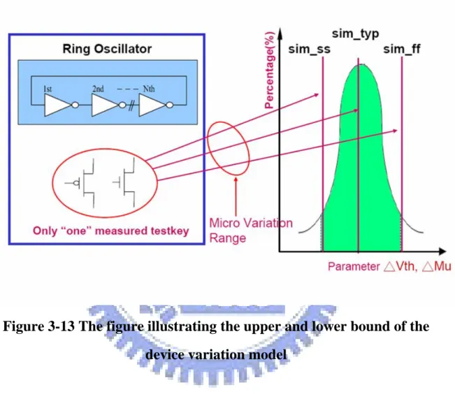
Figure 3-1 The devices locate on the eight spots on different glasses are measured and extracted for studying the variation---39 Figure 3-2 The figure illustrating the design issues as well as the device variation issue---40 Figure 3-3 (a) The figure illustrating the proposed crosstie layout. (b) The captured picture of the proposed layout ---41
Figure 3-4 (a) The VTH and (b) the mobility distribution of the measured crosstie devices for both n-type and p-type devices---42 Figure 3-5 The distribution of the device parameters with distance for (a) VTH and (b) mobility---43 Figure 3-6 The figure illustrating the large signal (long-range variation) and the small signal (micro variation) of the device parameters---44 Figure 3-7 The data and proposed model describing the VTH variation for the (a) n-type and (b) p-type devices---45 Figure 3-8 The data and proposed model describing the mobility variation for the (a) n-type and (b) p-type devices---46 Figure 3-9 The conventional structure of the differential pair circuit---47 Figure 3-10 (a) The simple distribution for the variable mapping. (b) A look up table for the variable mapping base---48 Figure 3-11 The cumulative distribution for the CMRR value of differential pair with different device parameter model---49 Figure 3-12 The photograph of the fabricated ring oscillator circuits---50 Figure 3-13 The figure illustrating the upper and lower bound of the device variation model ---51 Figure 3-14 The simulated and measured ring oscillator operating frequency with (a) operating voltage 5 V and (b) operating voltage 10 V---52 Figure 3-15 The interdigitated connection with different finger numbers---53 Figure 3-16 The VTH difference distribution of n-type devices in the interdigitated layout with different finger numbers---54 Figure 3-17 The VTH difference distribution of p-type devices in the interdigitated layout with different finger numbers---55 Figure 3-18 The mobility difference distribution of n-type devices in the interdigitated
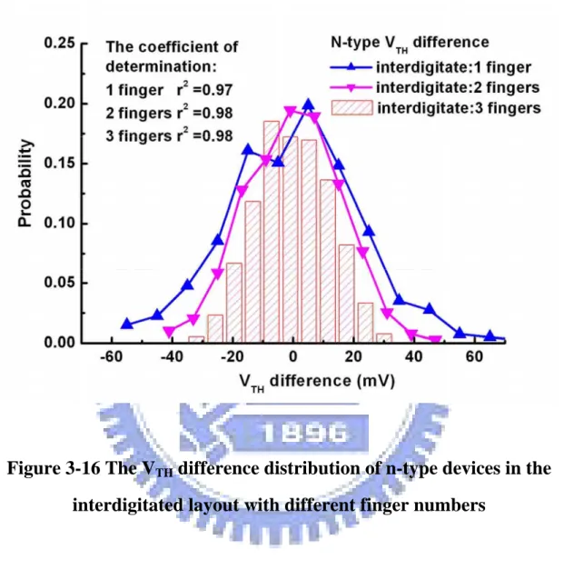
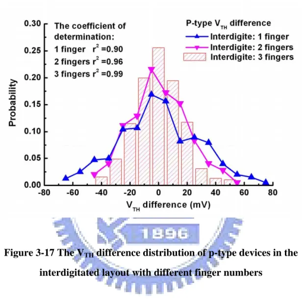
layout with different finger numbers---56 Figure 3-19 The mobility difference distribution of p-type devices in the interdigitated layout with different finger numbers---57 Figure 3-20 The standard deviation of the device parameter with different interdigit finger number for (a) VTH and (b) mobility---58 Figure 3-21 The log-scale standard deviation of the device parameter with interdigit finger number and the fitting curve for (a) VTH and (b) mobility---59 Figure 3-22 The standard deviation of VTH for different types of devices and for both n-type and p-type devices---60
Chapter 4
Figure 4-1 The threshold voltage shift under various stress conditions in the stress map---84 Figure 4-2 The ON current degradation under various stress conditions in the stress map---85 Figure 4-3 The threshold voltage, mobility and ON current for the LDD NMOS and PMOS devices under various stress conditions in the stress map---86 Figure 4-4 The profile of Joule heat generated in the channel for the device under self heating stress---87 Figure 4-5 The comparison for the heat transfer coefficients of the films for the poly- Si TFTs---88 Figure 4-6 The transfer characteristics for the n-type device after self heating stress-89 Figure 4-7 The density of states (DOS) for the device before and after self heating stress---90 Figure 4-8 The ON current degradation and the electric field for the device under hot carrier stress with various gate voltages---91
Figure 4-9 The ON current degradation for the device under hot carrier stress with
various drain voltages---92
Figure 4-10 The ON current degradation for the device under hot carrier stress with and without the LDD structure---93
Figure 4-11 The transfer characteristics for the n-type device after hot carrier stress-94 Figure 4-12 The transfer characteristics for the p-type device after hot carrier stress-95 Figure 4-13 The proposed mechanism for the increase of the mobility---96
Figure 4-14 The kick-back voltage in addressing the pixel voltage in TFT-LCD panels---97
Figure 4-15 The transfer characteristics for the fresh n-type device---98
Figure 4-16 The normalized capacitance curves for the fresh n-type device---99
Figure 4-17 The proposed circuit model for poly-Si TFTs---100
Figure 4-18 The RDS curves V.S. capacitance curves for the fresh device---101
Figure 4-19 The transfer characteristics for the n-type device before and after hot carrier stress---102
Figure 4-20 The normalized capacitance curves of (a) CGS and (b) CGD curves for the device before and after hot carrier stress---103
Figure 4-21 The normalized capacitance curves of (a) CGS and (b) CGD curves for the device after hot carrier stress with various measuring frequencies---104
Figure 4-22 The RDS curves V.S. the (a) CGS and (b) CGD curves for the device after hot carrier stress---105
Figure 4-23 (a) the proposed circuit model for the device after hot carrier stress and (b) the figure illustrating the corresponding location of Cdeg in the bandgap---106
Figure 4-24 The transfer characteristics for the n-type device before and after self heating stress---107 Figure 4-25 The normalized capacitance curves of (a) CGS and (b) CGD curves for the
device before and after self heating stress---108 Figure 4-26 The RDS curves V.S. the (a) CGS and (b) CGD curves for the device after self heating stress---109 Figure 4-27 (a) The proposed circuit model for the device after hot carrier stress and (b) the figure illustrating the corresponding location of the Cdeep in the bandgap and (c) the location of the Cdeg in the bandgap---111 Figure 4-28 The transfer characteristics for the fresh p-type poly-Si TFT---112 Figure 4-29 The normalized capacitance curves for the fresh p-type device---113 Figure 4-30 The RDS curves V.S. capacitance curves for the fresh p-type device----114 Figure 4-31 (a) The transfer characteristics and (b) the transconductance curves for the p-type device before and after hot carrier stress---115 Figure 4-32 The normalized capacitance curves of (a) CGS and (b) CGD curves for the p-type device before and after hot carrier stress---116 Figure 4-33 The RDS curves V.S. the (a) CGS and (b) CGD curves for the p-type device after hot carrier stress---117 Figure 4-34 The proposed circuit model for the p-type device after hot carrier stress---118 Figure 4-35 The transfer characteristics for the p-type poly-Si TFT before and after self heating stress---119 Figure 4-36 The normalized capacitance curves of (a) CGS and (b) CGD curves for the device before and after self heating stress---120 Figure 4-37 The RDS curves V.S. the (a) CGS and (b) CGD curves for the p-type device after self heating stress---121 Figure 4-38 The proposed circuit model for the p-type device after self heating stress---122
Chapter 5
Figure 5-1 Transfer characteristics and device mobility for the n-type device under the gate dynamic stress ranging between + 15 V and – 15 V--- 141 Figure 5-2 The emission microscope data for the device under gate dynamic stress ranging between + 15 V and – 15 V ---142 Figure 5-3 The model describing the mechanism for the degradation of n-type device under the gate dynamic stress ranging between + 15 V and – 15 V---143 Figure 5-4 Transfer characteristics and device mobility for the p-type device under the gate dynamic stress ranging between + 15 V and – 15 V---144 Figure 5-5 The model describing the mechanism for the degradation of p-type device under the gate dynamic stress ranging between + 15 V and – 15 V---145 Figure 5-6 A conventional pixel-addressing method for the TFT-LCD panels---146 Figure 5-7 The purpose for the stress conditions studied in this work---147 Figure 5-8 Transfer characteristics and device mobility for the n-type device after the gate dynamic stress ranging between 0 V and – 20 V with the grounded source and drain electrodes--- 148 Figure 5-9 Transfer characteristics and device mobility for the n-type device after the gate DC stress – 20 V with source and drain electrodes grounded---149 Figure 5-10 Normalized capacitance CGD for the n-type device after the gate dynamic stress ranging between 0 V and – 20 V---150 Figure 5-11 Normalized capacitance CGD for the n-type device after – 20 V gate DC stress--- 151 Figure 5-12 Mobility degradation for the n-type device after gate dynamic stress with different voltage range in (a) linear scale and (b) logarithmic scale---152 Figure 5-13 Mobility degradation for the n-type device after gate dynamic stress with different pulse frequencies--- 153
Figure 5-14 Mobility degradation for the n-type device after gate dynamic stress with different duty ratios---154 Figure 5-15 Transfer characteristics and device mobility for the p-type device under the gate dynamic stress ranging between 0 V and + 20 V with the grounded source and drain electrodes--- 155 Figure 5-16 Transfer characteristics and device mobility for the p-type device under the gate DC stress + 20 V with source and drain electrodes are grounded---156 Figure 5-17 Normalized capacitance CGD for the p-type device after gate dynamic stress ranging between 0 V and + 20 V---157 Figure 5-18 Normalized capacitance CGD for the p-type device after the gate DC stress + 20 V---158 Figure 5-19 Mobility degradation for the p-type device after gate dynamic stress with different voltage range shown in (a) linear scale and (b) logarithmic scale---159 Figure 5-20 Mobility degradation for the p-type device after gate dynamic stress with different pulse frequencies---160 Figure 5-21 Mobility degradation for the p-type device after gate dynamic stress with different duty ratios---161 Figure 5-22 Device cross section view and an equivalent circuit model for an n-type poly-Si TFT---162 Figure 5-23 Device cross section view and the band diagram for the gated p-i-n device---163 Figure 5-24 The figure showing how the voltage is picked to have only the N-side junction with large electric field---164 Figure 5-25 Normalized capacitance CGD for the gated p-i-n device after 200 second DC stress---165 Figure 5-26 The figure showing how the voltage is picked to have only the P-side
junction with large electric field ---166 Figure 5-27 Normalized capacitance CGD for the gated p-i-n device after 200 second DC stress---167 Figure 5-28 The figure discussing how the large electric field over the junctions could lead to the degradation---168 Figure 5-29 Transfer characteristics and device mobility for the n-type device before and after the DC hot carrier stress with stress duration 200 seconds---169 Figure 5-30 Normalized capacitance CGD for the n-type device before and after DC hot carrier stress---170 Figure 5-31 Transfer characteristics and device mobility for the p-type device after the DC hot carrier stress with stress duration 200 seconds---171 Figure 5-32 Normalized capacitance CGD for the p-type device before and after DC hot carrier stress---172 Figure 5-33 Transfer characteristics and device mobility for the n-type device before and after the drain DC stress with stress duration 200 seconds---173 Figure 5-34 Normalized capacitance CGD for the n-type device before and after drain DC stress---174 Figure 5-35 Transfer characteristics and device mobility for the p-type device before and after the drain DC stress with stress duration 200 seconds---175 Figure 5-36 Normalized capacitance CGD for the p-type device before and after drain DC stress---176 Figure 5-37 Transfer characteristics and device mobility for the n-type device before and after the gate AC stress toggling between ON/OFF regions---177 Figure 5-38 Normalized capacitance CGD for the n-type device before and after gate AC stress---178 Figure 5-39 Transfer characteristics and device mobility for the p-type device before
and after the gate AC stress toggling between ON/OFF regions---179 Figure 5-40 Normalized capacitance CGD for the p-type device before and after gate AC stress---180 Figure 5-41 Mobility degradation comparison for the n-type devices under various “generalized hot carrier stress” conditions---181 Figure 5-42 Mobility degradation comparison for the p-type devices under various “generalized hot carrier stress” conditions---182
Tables
Chapter 3
Table 3-1 The summarized average (AVG) and standard deviation (STD) value for (a) VTH and (b) mobility ---61 Table 3-2 The table illustrating the possible factors for long-range and micro variation as well as the corresponding design techniques---62 Table 3-3 The average and standard deviation value for the threshold voltage and mobility for the devices in the crosstie layout---63 Table 3-4 The upper and lower bound of the parameters used in the simulation of ring oscillator---64 Table 3-5 The standard deviation value for VTH and mobility with different interdigit finger number---65 Table 3-6 The fitting parameters and the coefficient of determination (r2) for fitting the standard deviation of interdigitated layout of poly-Si TFTs---66 Table 3-7 The fitting parameters and the coefficient of determination (r2) for fitting the standard deviation of interdigitated layout of various kinds of devices---67
Chapter 5
Table 5-1 The table summarizing the degradation behavior and dependency for the device under gate dynamic operation in the OFF region ---183
Chapter 1
Introduction
1-1 Overview of poly-Si TFT technology
Thin film transistor is a metal-oxide-semiconductor structure that can be fabricated on various kinds of substrates by using almost all kinds of deposition techniques [1-1]. Recently as for the substrates there have been the glass substrates, flexible substrates, stainless steel and so on. And as for the active region material, the film could be the silicon-based semiconductor, metal oxide and organic material [1-2]. The main feature of the TFT itself is the device can be formed upon various substrates and the material can be chosen from the applicable sources other than the high temperature single crystalline silicon wafer [1-3]. Such feature makes the TFT very suitable for the active display electronics since for each pixel the switching element is required and it is almost impossible for the single crystalline silicon device to be formed inside the respective pixel [1-4]. The first generation of active matrix liquid crystal displays (AMLCDs) used a-Si:H TFT as the pixel switching device. The main advantages of the a-Si:H TFT are the low process temperature (no higher than 600 degree Celsius) that can avoid damaging the glass substrate and the low leakage current that can avoid grey level shift as the TFT is turned off. However, the low electron field effect mobility (typically below 1 cm2V-1S-1) of a-Si TFTs limits the capability of advanced and integrated circuit. Integration of the driving circuit on display panel in parallel with the same substrate is very desirable not only to reduce the module cost but to improve the system reliability.
have attracted much attention because of their widely applications in active matrix liquid crystal displays (AMLCDs) and organic light-emitting diodes (OLEDs). Compare with a-Si:H TFTs, poly-Si TFT can provide higher electron mobility (by two orders of magnitude) and its higher driving current allows smaller TFT size to be used as the pixel-switching elements, resulting in higher aperture ratio and lower parasitic gate-line capacitance for improved display performance. In addition to flat panel displays, poly-Si TFTs have also been applied into some memory devices such as dynamic random access memories (DRAMs), static random access memories (SRAMs), electrical programming read only memories (EPROM), electrical erasable programming read only memories (EEPROMs). Among the poly-Si technologies, low temperature polycrystalline silicon thin-film transistors (LTPS TFTs) are primarily applied on glass substrate since higher process temperature may cause the substrate bent and twisted. Up to now, hundreds of researches have been reported to develop various technologies for improving the performance and reliability of LTPS TFTs. Since the electron field-effect mobility of LTPS TFTs is larger than a-Si:H TFTs but smaller than MOS transistors, it is expected that matured poly-si technology may realize several special functions such as the DAC (digital to analog converter), touch panels and sensors, even the memory and MPEG decoder as shown in figure 1-1[1-5]. Figure 1-2 shows the roadmap as for the expected development for the poly-Si TFTs as well as the integrated functions [1-5]. Researchers expect that as the mobility and the device performance keeps improving, the driver circuits and some special value-added functions can thus be formed by the use of poly-Si TFTs even for the lower performance CPU (Central processing Unit) and eventually form the system on glass (SOG) technology. In 2003 Sharp announced the prototype of the system on glass technology with the 8-bit CPU on it, as shown in figure 1-3 [1-6]. This somehow proved that for the display electronics the poly-Si TFTs can replace the
externally connected bond ICs and the perspective of the SOG technology is truly applicable.
1-2 Review and Motivation
Though the adoption of the poly-Si TFTs may be of beneficial, the devices are found to suffer serious variation, as shown in figure 1-4 [1-7]. Devices from predominant process condition still exhibit electrical behavior variation. Though the device structure is similar to MOSFETs, the variation behaviors of TFTs are much worse than those of MOSFETs. In the application using MOSFETs with high sensitivity to the mismatch variations such as current mirrors, digital-to-analog converters, and sense amplifiers, the statistical variation analysis would be a very important verification step. Owing to the low process temperature, poly-Si TFTs have different process from IC industry. Since the variation of device behavior may directly affect the circuit performance and reliability prediction, it would be of practical interest to have a clear understanding of how the variation may come and the behaviors the variation could be. In the scope of this thesis, since the poly-Si TFTs are capable of advanced circuitry and the perspective of SOG, the uniformity issue would become more critical. Another point of the study on device variation is that refer to the previous study the diversified device behavior would seriously affect the study of device reliability, and thus before studying the temporal variation it is required to find the devices with the variation effect as small as possible. In chapter 3 we studied the variation behavior as well as the effect of device variation on the circuit performance.
As for the temporal variation, it is also another point required to be deeply understood. From the practical viewpoint, the understanding of the reliability for the device under DC and AC operation can help designers to properly evaluate and estimate the practical device as well as the circuit performance. And as for the
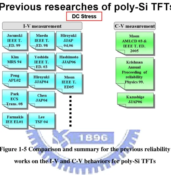
viewpoint of studying the mechanism, the deeper understanding of the mechanism can also help to devise methods to reinforce the device reliability. Though there are many papers on the I-V behaviors of poly-Si TFTs under DC stress, there are very few papers on the C-V behaviors for the device after DC stress, as shown in figure 1-5 [1-8]. In chapter 4, we would study the current transfer characteristics, namely the ID-VG curves, and the capacitance characteristics for the device under DC operation.
On the other hand, as for the device under AC operation, though in this case it would be more similar to the conditions in the real operations, there are not so many papers on it as in the case for the device under DC operation, in which the summary is given in figure 1-6 [1-9]. As for the AC operation, there are more parameters for the applied signal and it should be a good starting point to study the reliability for the conditions in applications. In real applications, the TFTs mainly act as the switches and thus the applied gate signal would toggle between the ON and OFF regions, in which the reliability for the devices had been reported by Uraoka [1-10]. However, there is still an important part that has not been reported and such operation condition occurs for most of the time in the pixel driving in the TFT-LCD panels. That is, the reliability for poly-Si TFTs under gate OFF region with the drain AC signals. In chapter 5 we studied the reliability behavior of the poly-Si TFTs under such operation conditions and proposed the model to describe it. The model is verified by using a special test structure and the discussion for the difference between the AC operation and the DC operation in the OFF region is also provided. Though the motivations for all the aforementioned three parts are all originated from the real applications, the mechanisms as well as the models should still provide valuable information for the designers from the viewpoints both of the real application and mechanism understanding.
1-3 Thesis Structure
There are six chapters in this dissertation, in which can be summarized in figure 1-7. First the poly-Si technology is introduced in chapter 1 and then the experimental, such as the fabrication and the measurement of the devices, is described in chapter 2. Then, we focus on the spatial variation first; the parameter distribution and the impact as well as the insights of the variation would be studied in chapter 3. Next, we study the temporal variation, in which the device behavior, namely the I-V and C-V behaviors after DC and AC operation, would be examined for both n-type and p-type devices and thereafter the similar circuit model is used to describe the degradation in chapter4 and 5. Chapter 6 gives the summaries and future work. The structure is in the other way listed below for indexing:
Chapter 1 Introduction
1-1. Overview of poly-Si TFT technology 1-2 Review and Motivation
1-3 Thesis Structure
Chapter 2 Experimental
2-1 Device Fabrication
2-2 Equipment and Experiment Setup
2-3 Extraction Methods of Device Parameters
Chapter 3 Characterization of Spatial Variation of Poly-Si TFTs
3-1 Review and Motivation
3-3 Impacts and Insights of Device Variation
3-3-1 Impacts of Device Variation on Circuit Performance 3-3-2 Insights of Device Variation
3-4 Summaries
Chapter 4 Characterization of Temporal Variation of Poly-Si TFTs: under DC Operation
4-1 Review and Motivation
4-2 Reliability Behavior under DC Operation: n-type Device 4-3 Reliability Behavior under DC Operation: p-type Device 4-4 Comparison and Discussion
4-5 Summaries
Chapter 5 Characterization of Temporal Variation of Poly-Si TFTs: under AC Operation
5-1 Review and Motivation
5-2 Reliability Behavior under Gate AC stress in the OFF Region: n-type Device 5-3 Reliability Behavior under Gate AC stress in the OFF Region: p-type Device 5-4 Comparison and Discussion
5-5 Summaries
Figure 1-1 The possible value-added functions for the
poly-Si TFT circuits
Figure 1-2 The roadmap and the perspectives for the
poly-Si TFT development
Figure 1-3 The system on glass prototype with the poly-Si TFT
technology from Sharp
Figure 1-4 Device parameters for poly-Si TFTs in which the serious
variation occurs
Figure 1-5 Comparison and summary for the previous reliability
works on the I-V and C-V behaviors for poly-Si TFTs
Figure 1-6 Comparison and summary for the previous works on the
reliability behaviors for poly-Si TFTs under DC and AC operation
Chapter 2
Experimental
Before going deep into the characterization of the poly-Si TFT, the experimental is described in this chapter. In section 2-1, the device fabrication flow is described. Next, the way how the device is measured and stressed and how the device parameters are extracted are explained.
2-1 Device Fabrication
The process flow of TFTs is described below. Top gate LTPS TFTs with width / length dimension of 20 µm / 5 µm were fabricated using low temperature process. Firstly, the buffer oxide and a-Si:H films with thickness of 50 nm were deposited on glass substrates with PECVD. The samples were then put in the oven for dehydrogenation. The XeCl excimer laser of wavelength 308 nm and energy density of 400 mJ/cm2 was applied. The laser scanned the a-Si:H film with the beam width of 4 mm and 98% overlap to recrystallize the a-Si:H film to poly-Si. After poly-Si active area definition, 100 nm SiO2 was deposited with PECVD as the gate insulator. Next, the metal gate was formed by sputter and then defined. For n-type devices, the lightly doped drain (LDD) and the n+ source/drain doping were formed by PH3 implantation with dosage 2 × 1013 cm-2 and 2 × 1015 cm-2 of PH3 respectively. The LDD implantation was self-aligned and the n+ regions were defined with a separate mask. The LDD structure did not use on p-type devices. The p+ source/drain doping was done by B2H6 self-align implantation with a dosage of 2 × 1015 cm−2. Then, the interlayer of SiNX was deposited. Subsequently, the rapid thermal annealing was conducted to activate the dopants. Meanwhile, the poly-Si film was hydrogenated.
Finally, the contact hole formation and metallization were performed to complete the fabrication work. The structure cross section view for the n-type poly-Si TFT is given is figure 2-1. The gated p-i-n devices, proposed to verify the validity of the reliability mechanism in chapter 5, are fabricated in parallel with the poly-Si TFTs to ensure the identical process condition.
2-2 Equipment and Experiment Setup
In this section, the equipments to measure the device characteristics, namely the transfer behavior ID-VG curves and the capacitance curves, are described. In addition, the apparatus to DC or AC stress the device as well as the AC pulse waveform is also illustrated.
The ID-VG curves for the devices are measured by the Agilent 4156A precision semiconductor parameter analyzer. The C-V curves of the gate-to-source capacitance CGS and gate-to-drain capacitance CGD before and after stress with different frequencies are measured with the HP 4284A precision LCR meter. The concept of operation of the apparatus is to find the effective impedance of equivalent circuit of the device under test between the probing nodes and via the circuit theory, the capacitance of the device can then be obtained. Before measuring the capacitance behavior, for every frequency the measure correction is performed with the open-circuit and short-circuit mode respectively for the needles before and after probing the electrode to eliminate the effect of the parasitic components in the surrounding and during probing.
The DC stress is performed by the Agilent 4156A precision semiconductor parameter analyzer, which is the same one to measure the transfer characteristics. The AC stress is performed by the Agilent 41501B pulse generator. Several parameters for the stress pulse are modulated to examine the dependence of device reliability on the
applied pulse parameters. The basic parameters of AC signal consists of frequency (f), signal high level (Vgh), signal low level (Vgl), high-level time (Vgh), low-level time (Vgl), rising time (Tr), and falling time (Tf). Fig. 2-2 shows the waveform of the AC signal. In AC signal, the definition of individual parameter is given as follow:
T = Tr + T_vgh + Tf + T_vgl f = 1/T Duty ratio = ( T_vgh )/T
and T is the signal period.
2-3 Extraction Methods of Device Parameters
Three important device parameters are extracted and studied in this work: the threshold voltage VTH, the sub-threshold swing S.S., and the field effect mobility Mu.
Plenty methods are used to determine VTH, which may be the most important parameter in application. In most of the researches on TFT, the constant current method is adopted. In this work the threshold voltage is determined by this method, which extract VTH from the gate voltage at the normalized drain current Id=10 nA for Vd=0.1V.
Sub-threshold swing, S.S (V/dec), is also a typical parameter to describe the control ability of gate toward channel. The sub-threshold swing should be ideally independent of drain voltage and gate voltage. However, in reality, the sub-threshold swing might increase with drain voltage due to short-channel effects. It might as well be affected by the serial resistance and interface traps and therefore become related to the gate voltage. In this work, it is defined as the minimum amount of gate voltage required to increase drain current by one order of magnitude.
transconductance gm at low drain voltage, which in this work 0.1 V is used. The transfer characteristics of poly-Si TFTs are similar to those of conventional MOSFETs, so the first order the first order I-V relation in the bulk Si MOSFETs can be applied to the poly-Si TFTs, which can be expressed as
] 2 1 ) [( 2 D D TH G ox FE D V V V V L W C I =μ − − (2-1) , where
Cox is the gate oxide capacitance per unit area,
W is channel width, L is channel length,
VTH is the threshold voltage.
If the drain voltage Vd is much smaller compared with (VG−VTH), then the drain
current can be approximated as:
D TH G ox FE D V V V L W C I =μ ( − ) .
And therefore the electron field effect mobility can be expressed as: gm D ox FE WV C L = μ
Where the transconductance is defined as:
D FE ox const V G D m V L WC V I g D
μ
= ∂ ∂ = = .n+
n+
Glass substrate
buffer oxide
interlayer
metal
Gate
n-
n-insulator
Figure 2-1 The cross section view of the n-type poly-Si TFTs
used in this work.
Figure 2-2 The figure illustrating the basic parameters
of the AC pulse
Chapter 3
Characterization of Spatial Variation of Poly-Si TFTs
3-1 Review and Motivation
As mentioned in chapter 1, poly-Si TFTs are expected to form the in-pixel switches and the integrated circuits for the display backplane electronics. Some value-added functions are also expected to be formed with the poly-Si TFTs [3-1]. For these circuits, panel designers need to evaluate the performance by the simulator with device model. The device model is expected to precisely describe the device behavior such that the simulation results can fit the real circuit performance as close as possible.
However, poly-Si TFTs are found to suffer from serious device behavior variation, which may not be well described by the model [3-2, 3-3]. So far though there are many papers on the design issues of the influenced circuit performance from the fluctuating poly-Si device behavior, there are very few papers on the variation behavior of poly-Si TFT itself [3-4~3-8]. Because its device structure is similar to MOSFETs (Metal-Oxide-Silicon Field Effect Transistors), it should be a good beginning to first review the variation behavior of MOSFETs and compare it to the case of poly-Si TFTs.
In MOSFETs, the device variation can be characterized as the local variation by short correlation distance and the global variations characterized by long correlation distances, where the correlation distance is defined as the distance in which a process disturbance affects the device performances [3-9]. If this distance is shorter than the usual distance between devices, the disturbance constitutes a local variation and affects few devices (e.g. a charge trapped in the gate oxide layer). For the global
variation, which is characterized by process disturbances with longer correlation distances (e.g. the gate oxide thickness fluctuation across the wafer surface), it affects all the devices within a specific region. Therefore, the devices placed at longer distance are more affected by global variations than devices placed close to each other. For the case of the poly-Si TFTs, since there are grains randomly located in the active region, the variation behavior may be more complicated than that in MOSFETs.
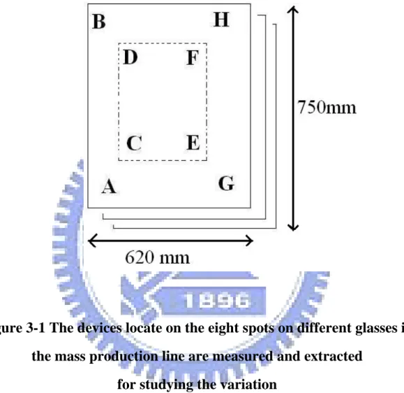
So how serious is this variation behavior of poly-Si TFTs? Refer to previous work, the parameters of the devices on the same spot from different glasses in the mass production line are measured and extracted and the values are given in the table below [3-10]. Table 3-1 gives the summarized values of the average (AVG) and the standard deviation (STD) for the threshold voltage VTH and mobility Mu for the devices located on the spot A to spot H on different glasses as shown in figure 3-1. Refer to the tables, the large standard deviation values of the parameters show that the devices suffer from serious variation problem and there is no apparent trend for such behavior. For example, if the film thickness variation dominates the variation, then the device parameter may show some kind of trend for the device located in the center part than those in the outer part. That is to say, for instance, the STD value would be larger for the devices on the C, D, E, and F spots than those on the A, B, G, H spots. Nevertheless, there is no such trend and the parameters for the eight spots just exhibit certain kind of random fluctuation. In other words, these parameters for the devices from the mass production line just somehow reveal that the variation behavior for the poly-Si TFTs truly exists and may not be neglected.
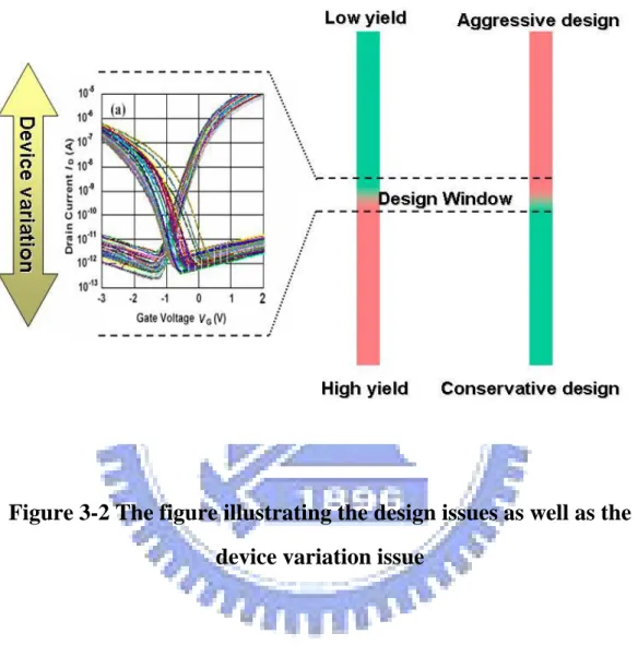
What does these SPC (Static Process Control) data mean to designers? First, as shown in figure 3-2, the serious variation for the devices means that in addition to the slim design window for the aggressive V.S. conservative design /low-yield V.S. high-yield design, the designers also need to design for the fluctuating device
performance. This would become an extra design issue and the corresponding over-design techniques could be difficult. For some applications, such as in the display panels as the poly-Si TFTs are most commonly applied, in some extreme cases designers even need to modify the circuit because of such serious device variation problem [3-11~3-12].
Another issue is that the true profile of the device variation itself is still not clear. From the SPC data designers could only get a rough idea about the range of the device variation on different glasses but the range and the behavior of the devices located near each other is still unknown. For example, in real applications circuit blocks usually contain devices locate within the range around several hundred micro-meters. In such cases the variation behavior could play an important role in the circuit performance and the aforementioned SPC data may not be applied. As mentioned before, the variation behavior could be different for the devices locate far away or close to each other. Therefore, it would be necessary to examine the variation behavior for the devices locate near each other since it could be more similar to the cases in real applications. Knowing the range and the behavior of the short-range variation would help designers to properly evaluate and estimate the circuit performance.
In light of the structure of this dissertation, there is still one point for the study of the spatial variation. Refer to previous works, the large device performance variation would greatly affect the examination of the device reliability [3-13]. Therefore, before the study of temporal variation, it would be necessary to somehow find the devices with small variation range to facilitate the following reliability study. In this chapter, section 3-2 focuses on the spatial variation and a similar table listing the possible variation sources for poly-Si TFTs is given. To avoid confusion, the local and global variations used in the notation of MOSFET variation are changed to long-range and
micro variation for poly-Si TFTs. A special layout is proposed to study the short-range variation and over 1000 devices in the layout are measured and the device parameters are extracted and summarized. A method inspired from the small signal concept in the electronics is utilized to decouple the long-range and micro-variation. The profiles for the micro variation of VTH and Mu are obtained and two equations are found to describe these profiles. Based on the two equations, the impacts of the device variation on the circuit performance are discussed in section 3-3-1, while the insights of the device variation behavior for different device dimension are discussed in section 3-3-2. The discussion and the summary for this chapter are given in section 3-4.
3-2 Classification and Characterization of Variation
For the case of poly-Si TFTs, the possible variation factors are given in table 3-2, in which the “ploy-Si grain size/number variation and grain boundary” are specially added to the micro variation factors. In order to investigate the relationship between uniformity issue and device distance, a special layout of the devices adopted in this work is shown in Fig 3-3 (a). This layout features the minimum distance that the two devices can locate, which is 40 micron meters when considering the design rules, and the captured picture of the proposed layout is shown in Fig. 3-3 (b). The structure of the poly-Si film and the gate metal are in the order that resembles the crosstie of the railroad and therefore afterward this layout is called the crosstie type layout of poly-Si TFTs. Within this short device distance, the long-range variation may be ignored, and the variation of device behavior can therefore be reduced to almost micro variation alone. In order to obtain the more accurate parameter distributions of crosstie layout TFTs, large amount of device parameters are required. In this work, more than one
thousand devices are measured and the parameters are extracted.
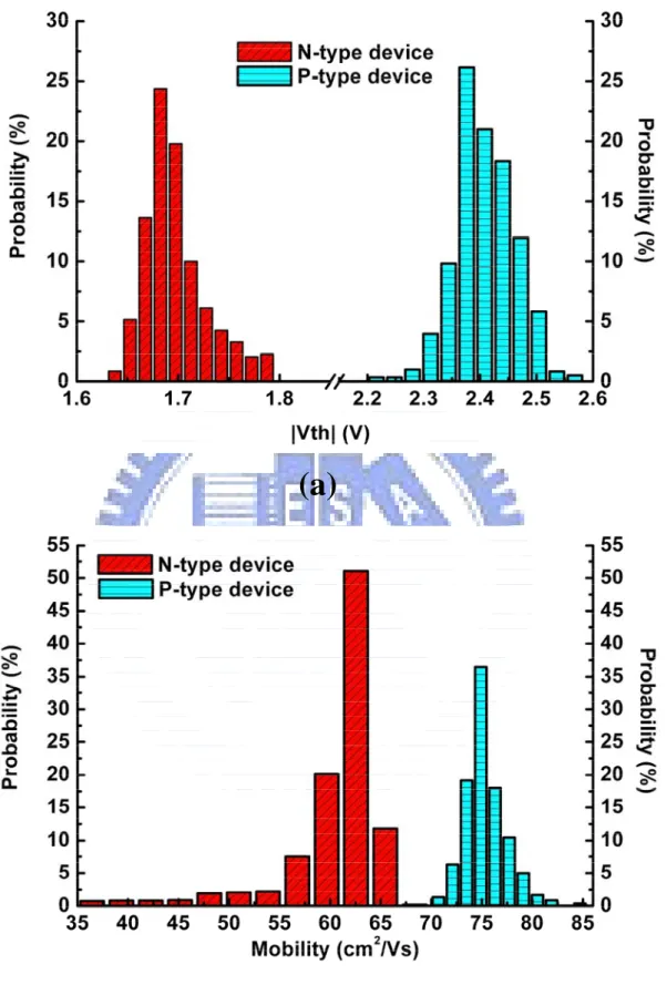
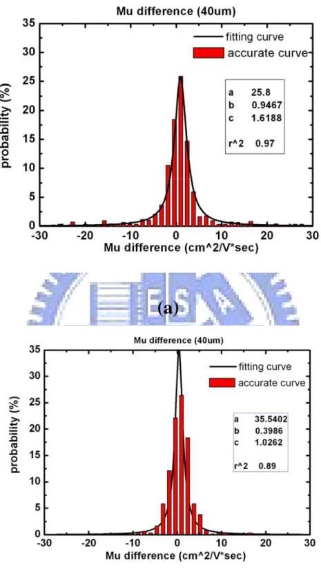
The distributions of threshold voltage (VTH) and mobility (Mu) for both the n-type and p-type TFTs are shown respectively in Fig. 3-4 (a) and (b). The average and the standard deviation values for device parameters of the TFTs are given in table 3-3. It can be seen that both Vth and mobility of the n-type and p-type TFTs do not follow the Gaussian distribution, which contradicts the usual expectation for the device parameter distribution. This reveals that the conventional Gaussian distribution may not be precise in describing device parameters. Besides, the distribution of mobility exhibits severe asymmetric behavior. Since the distributions are not symmetric, it would be difficult to build a model to describe the parameters for circuit simulation. In other words, another grouping method should be adopted.
Figure 3-5 (a) shows the VTH distribution of the devices with respect to device position, while figure 3-5 (b) shows that for mobility distribution. The distribution resembles the small signal concept in electronics. This means that the parameter distribution may be taken as the sum of the large signal and the small signal, as shown in figure 3-6. That is to say, the variation for poly-Si TFTs could be the long-range variation superimposed with a smaller value of micro variation. If the parameter difference is calculated within the two nearest devices, the large signal can then be subtracted and the true profile of the small signal can then be shown. In this case, the long-range variation can be diminished and the micro variation can then be investigated. The distribution of the VTH difference of the two nearest n-type TFTs and p-type TFTs are respectively shown in Fig. 3-7 (a) and (b), while that of the mobility difference for n-type and p-type devices are shown in Fig. 3-8 (a) and (b). The minimum distance of the devices is 40 um as shown in figure 3-3 (a). It can be seen that both the distributions of VTH and mobility difference for the devices show symmetric behavior and are quite centered than Gaussian distribution. This reveals
that micro variation may have a much concentric effect for the devices than Gaussian distribution.
Since the distributions of the parameter difference are symmetric, it would be necessary to find a model for circuit simulation. For the distribution of the difference of VTH, Gaussian-Lorentzian cross product is applied to the fitting, which is
(
)
2 2 - 1 1 *exp 1- * 2 a y x b x b d d c c = ⎛ ⎛ ⎞ ⎞ ⎛ ⎛ ⎞ + ⎜ ⎜ ⎟ ⎟ ⎜ ⎜ ⎟ ⎜ ⎝ ⎠ ⎟ ⎜ ⎝ ⎠ ⎝ ⎠ ⎝ - ⎞ ⎟⎟ ⎠ wherea is the peak value of the distribution b is the center of the distribution
c is fitting parameter related to the width of the distribution
d is fitting parameter varying from 0 to 1; 0 represent the pure Gaussain function and 1 means a pure Lorentzian distribution
As for the distribution of the difference of Mu, the Lorentzian distribution is applied to the fitting, which is
1 2 a y= x - b + c ⎛ ⎞ ⎜ ⎟ ⎝ ⎠ where
a is the peak value of the distribution b is the center of the distribution
c is fitting parameter related to the width of the distribution
In statistics, the coefficient of determination (R square) is a common index for evaluating the similarity between the proposed model and the real data. Generally, if the value of R square is above 0.7, it means that the specific model shows good agreement with the data [3-14]. In this work, the values of R square of the above
fittng curves, as shown in the figures, can both approach 0.9, representing the good validity between the proposed model and the real data. However, there could be still other equations that could provide higher fitness for describing the micro variation and the corresponding effects on circuit performance. Since the R square reaches above 0.9 for the two proposed models in describing the distribution, it could still be fair enough to use these models to evaluate the effect of device variation on both the circuits and also the study of the variation behavior for the devices with different dimension.
3-3 Impacts and Insights of Device Variation
In this section, based on the two proposed models to describe the device parameter variation, the impacts of device variation are discussed. The differential pairs and the ring oscillator, as the benchmarks of the digital and analog circuit, are adopted to study the influnces of device variation in section 3-3-1. On the other hand, by using the models the variation behavior for the device with different device width is also studied. With the help of the interdigitated layout, the variation behaviors for the poly-Si TFTs as well as the a-Si TFTs and single-crystal MOSFETs are examined and compared.
3-3-1 Impacts of Device Variation on Circuit Performance
(a) For the analog circuits: In the integrated circuit application, coupling effect
is a serious problem for signal transmission. Output signal suffering from serious coupling effect may lead to errors of the retrieved signal and affect the corresponding design window. In order to reinforce the immunity to the noise and the coupling effect during the transmission, the differential signals are widely used for analog circuit design. For the display applications, the differential pairs are commonly used in many
blocks of display electronics, such as the input stage of operational amplifier. Figure 3-9 shows the basic differential pair structure, where RD is the resistive load and Rss represents the output impedance of current bias; differential signals are applied to the gate terminal of transistor M1 and M2.
The quality of data transmission will benefit by the use of differential signal. However, device variation would be a serious problem for differential pair. Since these devices are nominally identical, the variation of the device characteristics will result in errors in retrieving the signal and affect the accuracy of the differential signal. In conventional MOSFET circuits, the variation between M1 and M2 is very low and can be suppressed under the well-controlled process. As compared to CMOS technology, poly-Si TFTs suffer form worse device variation and the effect of output signal variation may hence be more complicated. In order to evaluate the circuit performance of differential pair by poly-Si TFTs, the aforementioned variation models would be adopted to simulate the circuit performance with device variation.
The common mode rejection ratio (CMRR) is a common index for the capability of differential pair against the common mode noise, which can be written as
2 2 GS th (V -V A μ ox GS th dm cm-dm th GS th W ) 2 C (V -V ) Rss L CMRR A V (V -V ) μ μ μ + = ≅ Δ + Δ
In the equation above, the ΔVth and Δµ terms represent the differences of threshold voltage and mobility of the two transistors. In this work, the CMRR value is used as the index to examine the accuracy of each simulation skill and model.
Before the simulation, it is essential to transform the parameter distribution into the corresponding value for Monte Carlo simulation. In this work, a method of range mapping is used. Take the distribution consisting of four variables as example, as
shown in figure 3-10 (a). Based on the probability, a table of range mapping can be established, as shown in figure 3-10 (b). For a series of uniformly random values in the range from 0 to 1 generated by the computer, the corresponding series can be obtained by looking up table in figure 3-10 (b). If 0.3 is randomly picked from computer, the variable B will be chosen according to Fig. 3-10 (a). Thus, the distribution from the look-up values will match that shown in figure 3-10 (a). In light of statistics thoery, a certain number of data for each distribution can be generated to get the stable and reliable simulation result. In this work, 210,000 times of data transformation for each distribution are executed to obtain the best and stable result for the Monte Carlo simulation.
In simulation, the VGS is set to 5V, which is the voltage at the quiescent point. The output impedance of current bias is 3 MΩ, which is extracted from the output resistance at the corresponding bias point. To compare the effects of the device variation on circuit performance with different models, two distribution models are adopted in the Monte Carlo simulation to calculate the CMRR value under the constant device distance of 200 µm. One is the extracted distribution and the other is the widely-adopted Gaussian distribution. The parameters of Gaussian distribution used here are 1.69V, 0.03V, 59.66 cm2/Vs and 7.84 cm2/Vs, which respectively correspond to the mean value and the deviation of the threshold voltage and mobility from the measured database as shown in table 3-3.
The simulation of the cumulative distribution of the CMRR value in dB is shown in Fig. 3-11. The results of Monte Carlo method with Gussian distribution and the real extracted distribution are represnted by lines with circles, squares and triangles individually. The line with circle symbols is plotted by Monte Carlo method with Gussian distribution. As for the line with squares and triangles, they are done by Monte Carlo method with the extracted distribution. For the line with squares, the