具基體雜訊考量之射頻電壓控制振盪器電路設計
84
0
0
全文
(2) 具基體雜訊考量之射頻電壓控制振盪器電路設計. CMOS RF VCO Design with Substrate Noise Consideration. 研 究 生 : 簡志松 指導教授 : 柯明道. Student : Chih-Sung Chien 教授. Advisor : Ming-Dou Ker. 國立交通大學 電子工程學系 電子研究所碩士班 碩士論文 A Thesis Submitted to Institute of Electronics College of Electrical Engineering and Computer Science National Chiao-Tung University In Partial Fulfillment of the Requirements For the Degree of Master of Science In Electronic Engineering. March 2005 Hsinchu, Taiwan. 中華民國九十四年三月.
(3) 具基體雜訊考量 之射頻電壓控制振盪器電路設計 研究生: 簡志松. 指導教授: 柯明道 博士. 國立交通大學 電子工程學系 電子研究所碩士班. 摘要 本論文主旨在探討不同結構的變容器對於基體雜訊的隔絕能力。就標準互 補式金氧半導體製程而言,有四種金氧半導體結構可以作為變容器,而且這四種 變容器都具有可以隔絕基體雜訊的特定結構。本論文的第二章將探討與比較這四 種變容器的高頻特性。 這四種變容器中,其中兩種生成於 n 型井上且利用介於 n 型井與基體的 p-n 接面隔絕基體雜訊;另外兩種生成於 p 型井上且被深層 n 型井與 n 型井所包圍以 隔絕基體雜訊。本論文的第三章將比較這兩種結構對於基體雜訊的隔絕能力。 在本論文的第五章中,我們利用 0.25 微米互補式金氧半導體製程設計且實 現了三個操作在 2.4GHz 頻段的電感電容共振型電壓控制振盪器電路。VCO1 與 VCO2 唯一不同的地方在於所使用的變容器,這兩種變容器以不同的結構來隔絕 基體雜訊。將訊號產生器提供的一個射頻訊號注入基體中作為基體雜訊,我們將 探討耦合至變容器的基體雜訊對於 VCO1 與 VCO2 輸出頻譜的影響。VCO1 與 VCO3 採用相同結構的電感與變容器但是不同的電路架構,我們將利用 VCO1 與 VCO3 來比較不同電路架構的相位雜訊。 i.
(4) CMOS RF VCO Design with Substrate Noise Consideration Student: Chih-Sung Chien. Advisor: Prof. Ming-Dou Ker. Department of Electronics Engineering & Institute of Electronics, National Chiao-Tung University. Abstract The isolation capabilities of varactors with different structures against substrate noise are investigated in this thesis. In chapter 2, four types of MOS structure varactor available in standard CMOS processes are investigated. They all have specific structures able to isolate substrate noise. High-frequency characteristics of them are compared. Among these four varactors, two of them are fabricated on n-well and use the p-n junction between n-well and substrate to isolate substrate noise. The other two are fabricated on p-well and surrounded by deep n-well and n-well in order to isolated substrate noise. Isolation capabilities of different isolation structures are compared in chapter 3. In chapter 5, three 2.4GHz LC VCO circuits are designed and realized in a 0.25-um CMOS process. VCO1 and VCO2 differ only in the type of varactor. An RF signal provided by signal generator is injected into the substrate as substrate noise. The influences of substrate noise coupling to the varactors on the output spectrums of VCO1 and VCO2 are investigated. VCO1 and VCO3 use the same type of inductor and varactor, but they differ in the type of circuit topology. The phase noise of them is compared.. ii.
(5) 誌謝. 本論文得以順利完成,首先我要感謝指導教授 柯明道老師於研究上的指 導,並且提供研究所需的資源。此外,也要感謝諸位口試委員對論文的指正與建 議。 感謝國家奈米元件實驗室高頻量測中心提供高頻量測相關的儀器及晶片量 測上的協助。 感謝實驗室的陳世倫學長及陳榮昇學長在研究過程中給予的協助。感謝林 昆賢學長在晶片下線時給予的協助。 感謝多年的室友及棒球隊的隊友這一路上的陪伴。 最後,我要感謝我的父母及家人,因為你們的支持與關心,使我得以順利 完成學業。. iii.
(6) CONTENTS ABSTRACT (CHINESE). i. ABSTRACT (ENGLISH). ii. ACKNOWLEDGEMENTS. iii. CONTENTS. iv. TABLE CAPTIONS. vii. FIGURE CAPTIONS. viii. Chapter 1 Introduction 1.1. Background. 1. 1.2. Motivation. 3. 1.3 Organization of This Thesis. 4. Chapter 2 High-Frequency Characteristics of Varactors 2.1. Varactor Structures. 7. 2.1.1 General Consideration. 7. 2.1.2. P-N Junction Varactor. 7. 2.1.3 N-type MOS Varactor. 8. 2.1.4. P-type MOS Varactor with Deep N-well. 8. 2.1.5. NMOS Varactor with Deep N-well. 9. 2.1.6. PMOS Varactor. 9. 2.1.7. Discussion on Varactors. 10. 2.2. Layout Designs. 11. 2.3. Measurement Setup. 12. 2.4. Pad De-Embedding. 12 iv.
(7) 2.4.1 Pad De-Embedding Procedure. 12. 2.4.2 Discussion on Pad De-Embedding Methods. 14. 2.5. Equivalent Circuit Model. 15. 2.6. Measurement Results. 15. Chapter 3. Substrate Noise Isolation Test. 3.1. The Structures of Testkeys. 29. 3.2. Measurement Results. 29. Chapter 4 Design Considerations for LC-tank VCOs 4.1 LC-tank VCO Basics. 34. 4.2. 35. Phase Noise 4.2.1. Definition. 35. 4.2.2 Conversion of Noise to Phase Noise. 4.2.3. 35. 4.2.2.1 Noise Mixing and Noise Folding. 35. 4.2.2.2 Frequency Modulation. 36. Phase noise model. 38. 4.3 LC-tank VCO Topologies. 39. 4.4. 40. Output Buffer. Chapter 5 Circuit Designs and Implementation 5.1 Circuit Designs. 47. 5.2. 48. Simulation Results. 5.3 Layout Designs. 48. 5.4. 49. Measurement Results. Chapter 6 6.1. Conclusions and Future Works. Conclusions. 67. v.
(8) 6.2. Future works. 67. References. 69. vi.
(9) TABLE CAPTIONS Chapter 2 Table 2.1 The comparison of the measured characteristics of different MOS structure varactors. Chapter 5 Table 5.1 A summary of the measured and simulated results of VCO1 Table 5.2 A summary of the measured results of VCO2 Table 5.3 A summary of the measured and simulated results of VCO3. vii.
(10) FIGURE CAPTIONS Chapter 1 Fig. 1.1. Generic transceiver architecture.. Fig. 1.2. Basic phase-locked frequency synthesizer.. Fig. 1.3. (a) Isolation structure for varactors fabricated on n-well and (b) Isolation structure for varactors fabricated on p-well with deep n-well.. Chapter 2 Fig. 2.1. Cross section of p-n junction varactor.. Fig. 2.2 Cross section of n-type MOS varactor. Fig. 2.3. Cross section of p-type MOS varactor with deep n-well.. Fig. 2.4 Cross section of NMOS varactor with deep n-well. Fig. 2.5. Cross section of PMOS varactor.. Fig. 2.6. The layouts of (a) test structure of n-type MOS varactor, (b) the corresponding de-embedding OPEN structure, and (c) the device.. Fig. 2.7. The layouts of (a) test structure of p-type MOS varactor with deep n-well, (b) the corresponding de-embedding OPEN structure, and (c) the device.. Fig. 2.8. The layouts of (a) test structure of NMOS varactor with deep n-well, (b) the corresponding de-embedding OPEN structure, and (c) the device.. Fig. 2.9. The layouts of (a) test structure of PMOS varactor, (b) the corresponding de-embedding OPEN structure, and (c) the device.. Fig. 2.10. The parasitic components originating from the contact pads.. Fig. 2.11 The complete equivalent circuit of the RF test structure [8][9]. Fig. 2.12. The measured Cs and the simulated Cs of n-type MOS varactor at 100MHz. viii.
(11) Fig. 2.13. The measured Cs and the simulated Cs of n-type MOS varactor at 2.5GHz.. Fig. 2.14. The measured Cs and the simulated Cs of n-type MOS varactor at 5GHz.. Fig. 2.15. The measured Cs and the simulated Cs of n-type MOS varactor at 10GHz.. Fig. 2.16. The simulated Cs of n-type MOS varactor at 100MHz, 2.5GHz, 5GHz, and 10GHz respectively.. Fig. 2.17. The measured Q and the simulated Q of n-type MOS varactor at 2.5GHz.. Fig. 2.18. (a) The layout of the test structure with the DUT. (b) Magnified view of the layout of the de-embedding structures. The pad layout and interconnection layout are equal to the test structure.. Fig. 2.19. The measured Cs of n-type MOS varactor at 2.5GHz.. Fig. 2.20. The measured Cs of p-type MOS varactor with deep n-well at 2.5GHz.. Fig. 2.21. The measured Cs of NMOS varactor with deep n-well at 2.5GHz.. Fig. 2.22. The measured Cs of PMOS varactor at 2.5GHz.. Chapter 3 Fig. 3.1. The isolation testkey corresponding to n-type MOS varactor and PMOS varactor.. Fig. 3.2. The isolation testkey corresponding to NMOS varactor with deep n-well and p-type MOS varactor with deep n-well. Fig. 3.3. The measured S 21 parameters of the testkey shown in Fig. 3.1. The n-well is biased at 0V, 1.25V, and 2.5V respectively.. Fig. 3.4. The measured S 21 parameters of the testkey shown in Fig. 3.2. The deep n-well is biased at 0V, 1.25V, 2.5V, and floating respectively.. Fig. 3.5. The comparison of the isolation capability of different isolation structures. The n-well in Fig. 3.1 is biased at 0V. The deep n-well in Fig. 3.2 is biased at 2.5V. ix.
(12) Fig. 3.6. The comparison of the isolation capability of different isolation structures. The n-well in Fig. 3.1 is biased at 2.5V. The deep n-well in Fig. 3.2 is biased at 2.5V.. Chapter 4 Fig. 4.1 Feedback oscillatory system with frequency-selective network. Fig. 4.2. (a) One port view of oscillators, (b) LC resonator, and (c) equivalent circuit of (b).. Fig. 4.3. Output spectrum of ideal and actual oscillators.. Fig. 4.4. Phase noise in (a) signal path, and (b) control path.. Fig. 4.5 Noise shaping in oscillators. Fig. 4.6. Noise folding in an oscillator.. Fig. 4.7 Modulation of VCO frequency by noise on control line. Fig. 4.8. Phase noise spectrum according to Leeson-Cutler phase noise model.. Fig. 4.9. (a) PMOS-only topology, (b) NMOS-only topology, and (c) complementary topology.. Chapter 5 Fig. 5.1. The circuit topology of VCO1 and VCO2.. Fig. 5.2 The top view and physical dimension of spiral inductor. Fig. 5.3. The circuit topology of VCO1 and VCO2 with substrate noise injection, and the Bias Tees are not drawn.. Fig. 5.4. The circuit topology of VCO3.. Fig. 5.5. The layout of VCO1.. Fig. 5.6. The layout of VCO2.. x.
(13) Fig. 5.7. The layout of VCO3.. Fig. 5.8. The measured output spectrum of VCO1 at 1.9358-GHz oscillation frequency.. Fig. 5.9. The measured and simulated oscillation frequency of VCO1 versus the control voltage Vcont .. Fig. 5.10. The measured phase noise of VCO1 at 1.9368-GHz carrier frequency.. Fig. 5.11 The measured output spectrum of VCO2 at 2.548-GHz oscillation frequency. Fig. 5.12. The measured oscillation frequency of VCO2 versus the control voltage Vcont .. Fig. 5.13. The measured phase noise of VCO2 at 2.5493-GHz carrier frequency.. Fig. 5.14. The measured output spectrum of VCO3 at 2.2327-GHz oscillation frequency.. Fig. 5.15. The measured and simulated oscillation frequency of VCO3 versus the control voltage Vcont .. Fig. 5.16. The measured phase noise of VCO3 at 2.4333-GHz carrier frequency.. Fig. 5.17. In VCO1, at 2.499-GHz oscillation frequency, (a) the measured output spectrum without substrate noise injection and (b) the measured output spectrum with substrate noise injection.. Fig. 5.18. In VCO2, at 2.5713-GHz oscillation frequency when the deep n-wells of NMOS varactors are biased at 2.5V, (a) the measured output spectrum without substrate noise injection and (b) the measured output spectrum with substrate noise injection.. Fig. 5.19. In VCO2, at 2.5692-GHz oscillation frequency when the deep n-wells of NMOS varactors are biased at 0V, (a) the measured output spectrum without substrate noise injection and (b) the measured output spectrum xi.
(14) with substrate noise injection. Fig. 5.20. In VCO2, at 2.5686-GHz oscillation frequency when the deep n-wells of NMOS varactors are floating, (a) the measured output spectrum without substrate noise injection and (b) the measured output spectrum with substrate noise injection.. Fig. 5.21. In VCO2, when power supply is off, the measured output spectrum with substrate noise injection.. xii.
(15) Chapter 1 Introduction. 1.1 Background Recently, there has been considerable interest in the use of standard CMOS processes to implement RF transceiver components such as low-noise amplifiers (LNAs), mixers, and voltage-controlled oscillators (VCOs). The benefit is the potential for achieving high-levels of RF/analog/digital integration, rapidly approaching single-chip system implementations. VCOs are key components of RF transceivers for wireless communications. The VCOs used in RF transceivers are usually embedded in a frequency synthesizer so as to generate a precise definition of the local oscillator (LO) signal for upconversion from and downconversion to the baseband. The role of frequency synthesizer in generic transceiver is illustrated in Fig. 1.1 [1]. The frequency synthesizer is conceptually a phase-locked loop. There are several frequency synthesizer architectures, including integer-N, fractional-N, and direct-digital synthesis techniques. Fig. 1.2 shows the architecture of a basic phase-locked frequency synthesizer. The channel control input is a digital word that varies the value of M. Since fout = MfREF , the relative accuracy of fout is equal to that of fREF . For this reason, fREF is derived from a stable, low-noise crystal oscillator [2]. Inductance-capacitance (LC) tank oscillator is a superior choice due to the inherent bandpass filtering of the LC resonator which can suppress side-band noise. Thus, for monolithic integration in CMOS, LC-tank VCOs are preferred over ring oscillators which are easier to integrated and less area consuming. -1-.
(16) Despite the continuous improvement, VCOs still remain the bottleneck and, thus, the main challenge of RF transceivers. This is due to the combination of very demanding VCO parameters: low phase noise, low power consumption, and large frequency tuning range. In LC-tank VCOs, phase noise and power consumption depend primarily on the quality factor (Q) of the tank. The frequency tuning range is determined by the capacitance tuning range of the varactor (voltage-dependent capacitor) and parasitics in the VCO. Hence, a main task is to optimize the performance of inductors and varactors. Monolithic inductors are usually implemented as spiral structures in the use of thick top metal in standard CMOS processes. Due to large energy loss to the substrate, they feature poor Q, compared to the varactors realized in standard CMOS processes. Therefore, it is expected that, independent of the type of varactor, the spiral inductor will determine the worst-case Q of the LC-tank and the worst-case phase noise of the VCO [3]. The Q of the inductor is defined as ωL/R s . A circular spiral inductor exhibits less metal resistance and thus higher Q for a given value of inductance and metal wire width. Despite extensive recent work, the Q of the inductors in standard CMOS processes has been limited to low value. Thus, the monolithic inductors still limits the phase-noise performance of fully integrated LC-tank VCOs. Research on monolithic inductors nevertheless continues. The frequency tuning range of the LC-tank VCO is determined by the capacitance tuning range of the varactor in the VCO. VCO parasitics will deteriorate the effective tuning capabilities of the varactors. Further, process variations in the varactor itself and in the inductors need to be compensated. Therefore, the varactors with wide capacitance tuning range are required to guarantee specified center frequency and frequency tuning range. The varactor structures available in standard CMOS processes are p-n junction varactor and MOS structure varactors. The -2-.
(17) capacitance value of the p-n junction varactor is controlled by the reverse-bias voltage. The technology scaling lowers the maximum circuit supply voltage and the maximum usable diode reverse-bias voltage. Therefore, the technology scaling decreases the capacitance tuning range of the p-n junction varactor. Tuning with the MOS structure varactors is the more promising approach. Strong capacitance variation within a few hundreds of millivolts makes the MOS structure varactors useful at low supply voltage [4].. 1.2 Motivation Most modern CMOS processes use a heavily-doped p+ substrate to minimize latch-up susceptibility. However, the low resistivity of the substrate (on the order of 0.1 Ω ⋅ cm) creates unwanted paths between various components in the same substrate, thereby corrupting sensitive components. Some people call this “substrate noise” because the unwanted signals from other components are a kind of noise. However, this noise has quite different physic meaning from the thermal noise, flicker noise, or shot noise. Substrate noise resulting from other components, propagating in the substrate, and coupling to the varactors will affect the output spectrums of the VCOs. Of course, substrate noise also couples to the other constituent devices (transistors, and inductors) in the VCOs and thus influences the output spectrums. In this thesis, we focus on the influences of substrate noise coupling to the varactors on the output spectrums of the VCOs. The varactors fabricated on n-well can use the p-n junction between substrate and n-well to isolate substrate noise. Because of no isolation between p-well and substrate, it is obvious that the varactors fabricated on p-well are more sensitive to substrate noise. However, deep n-well can provide isolation between p-well and substrate for the varactors fabricated on p-well. In general, deep n-well is offered in. -3-.
(18) deep-submicrometer CMOS processes for better substrate noise isolation of p-well devices because of an additional p-n junction. Therefore, there are two types of isolation structure for varactors in standard CMOS processes (Fig. 1.3). In this thesis, the testkey-level method is used to verify which structure has better isolation capability by comparing the measured S 21 parameters. The details of the testkey-level method are described in chapter 3. Furthermore, two 2.4GHz LC-tank VCOs (VCO1 and VCO2) are realized to investigate the influences of substrate noise coupling to the varactors on the output spectrums of the VCOs. VCO1 and VCO2 differ only in the type of varactor: n-type MOS varactor (VCO1) and NMOS varactor with deep n-well (VCO2). An RF signal injected into the substrate as substrate noise is provided by signal generator. The RF signal is injected into the substrate through the p+ ring surrounding the varactors. The details are described in chapter 5.. 1.3 Organization of This Thesis This thesis is organized as follows. In chapter 2, four types of MOS structure varactor are realized and the high-frequency characteristics of them are compared. In chapter 3, two testkeys corresponding to different isolation structures are designed to verify which structure has better isolation capability. The measured S 21 parameters of the testkeys are shown. In chapter 4, design considerations for LC-tank VCO are discussed. In chapter 5, Three 2.4GHz LC-tank VCOs (VCO1, VCO2, and VCO3) are designed and realized in a 0.25-um CMOS process. VCO1 and VCO2 are realized to investigate the influence of substrate noise coupling to the varactors on the output spectrums. VCO3 adopting complementary topology is designed to compare with VCO1 adopting PMOS-only topology. The phase noise of them is compared. In chapter 6, the conclusions and future works are given.. -4-.
(19) LNA. Band Pass Filter. Frequency Synthesizer. Duplexer Filter. PA. Fig. 1.1. Band Pass Filter. Generic transceiver architecture.. fREF. PFD. CP/LPF. ÷M Channel Selection. Fig. 1.2. Channel Selection. Basic phase-locked frequency synthesizer. -5-. VCO. f out.
(20) n-well. p-well. p-well. p-substrate. (a). Vb n+. p-well n-well. p-well. n-well p-well. deep n-well p-substrate (b) Fig. 1.3 (a) Isolation structure for varactors fabricated on n-well and (b) Isolation structure for varactors fabricated on p-well with deep n-well. -6-.
(21) Chapter 2 High-Frequency Characteristics of Varactors. 2.1 Varactor Structures 2.1.1. General Considerations. Design considerations for varactors are summarized as follows [5]: (1) A high quality factor. (2) A control voltage range compatible with the supply voltage, ultimately 1 V for single battery cell operation. (3) A good tunability over the available control voltage range. (4) A small silicon area, to reduce cost. (5) A reasonably uniform capacitance variation over the available control voltage range, to make the phase-locked-loop design easier. Two classes of devices have to be considered: junction structure and MOS (metal-oxide-semiconductor) structure varactors, the latter tuning the capacitance by changing the operation regions (accumulation region, inversion region, and depletion region). In all cases, the devices should be placed in separated wells in order to use the p-n junction between substrate and n-well to isolate substrate noise. The five types of device are therefore p-n junction varactor, n-type MOS varactor (accumulation mode), p-type MOS varactor with deep n-well (accumulation mode), NMOS varactor with deep n-well, and PMOS varactor. The details are described as follows.. 2.1.2. P-N Junction Varactor. The cross section of p-n junction varactor is shown in Fig. 2.1. The p-n junction used as varactor must be operated in reverse-biased region and the capacitance value -7-.
(22) is controlled by the reverse voltage.. 2.1.3. N-type MOS Varactor. The cross section of n-type MOS varactor (accumulation mode) is shown in Fig. 2.2. This structure is widely used as varactor in standard CMOS processes. The device capacitance is given by C = C 0 WL , where C 0 is given by −1. ⎛ 1 1 ⎞ ⎟⎟ , C 0 = ⎜⎜ + ⎝ C OX C d ⎠. (2.1). in which C OX and C d are, respectively, the oxide capacitance and the capacitance of the depletion layer under the gate, per unit area. By applying a positive voltage between the gate (Vgate ) and the source/drain (Vcont ) the surface is accumulated and the device capacitance equals the oxide capacitance. If the applied voltage is reversed, the surface layer is depleted and the series capacitance decreases. The maximum capacitance (C max ) , per unit area, of the device corresponds to a heavily accumulated surface and equals C OX = ε/t OX . On the other side, a minimum value. (Cmin ). is reached when the voltage difference between the electrodes equals the. threshold voltage. Beyond this point, an inversion layer is formed under the gate. At low frequency this effect brings the value of the device capacitance close to the gate oxide capacitance. At high frequency, where the varactor is assumed to be operated, this effect is not seen and the device capacitance remains at its minimum value. The ratio between C max and Cmin defines the tuning range [4].. 2.1.4. P-type MOS Varactor with Deep N-well. The cross section of p-type MOS varactor with deep n-well (accumulation mode) is shown in Fig. 2.3. Deep n-well and n-well surrounding the p-well isolate this device from substrate noise. By applying a negative voltage between the gate (Vgate ) -8-.
(23) and the source/drain (Vcont ) the surface is accumulated and the device capacitance equals the oxide capacitance. If the applied voltage is reversed, the surface layer is depleted and the series capacitance decreases. The maximum capacitance (C max ) , per unit area, of the device corresponds to a heavily accumulated surface and equals C OX = ε/t OX . On the other side, a minimum value (Cmin ) is reached when the voltage difference between the electrodes equals the threshold voltage. Beyond this point, an inversion layer is formed under the gate. At low frequency this effect brings the value of the device capacitance close to the oxide one. At high frequency, where the varactor is assumed to be operated, this effect is not seen and the device capacitance remains at its minimum value. This device has the advantage of a lower parasitic resistance than n-type MOS varactor mentioned in section 2.1.3.. 2.1.5. NMOS Varactor with Deep N-well. The cross section of NMOS varactor with deep n-well is shown in Fig. 2.4. Deep n-well and n-well surrounding the p-well isolate this device from substrate noise. This device is a three-terminal device. These three terminals are gate. (V ) , gate. source/drain (Vcont ) , and bulk respectively. The device capacitance is relative to not only the voltage difference between gate and bulk but also the bias voltage of source/drain. It should be noted that, with floating source/drain terminal and using bulk terminal as control voltage node, this device can work like p-type MOS varactor with deep n-well mentioned in section 2.1.4.. 2.1.6. PMOS Varactor. The cross section of PMOS varactor is shown in Fig. 2.5. This device works in the strong, moderate, or weak inversion region only, and never enters the. -9-.
(24) accumulation region. Since the bulk is connected to the power supply VDD , the device does not enter the accumulation region and remains in the weak inversion region for a very wide range of positive voltage between the gate (Vgate ) and the source/drain. (Vcont ). [6]. When the voltage difference between the gate and the source/drain is. smaller than the threshold voltage, the device enters the strong inversion region and the device capacitance, per unit area, equals C OX = ε/t OX .. 2.1.7. Discussion on Varactors. Since the p-n junction varactor is realized in an n-well isolated from the substrate, both ports can be biased above ground. When the p-n junction varactor is used in a VCO circuit, the p+ contact must be connected to the “signal” electrode and the n+ contact must be connected to the “control voltage” electrode to get rid of the n-well to substrate capacitance. When MOS structure varactors are used in a VCO circuit, the gate (Vgate ) must be connected to the “signal” electrode and the source/drain (Vcont ) must be connected to the “control voltage” electrode to get rid of the effect of the parasitic capacitance seen from the source/drain node to AC ground node. For n-type MOS varactor, the parasitic capacitance is the n-well to substrate capacitance. For NMOS varactor with deep n-well, the parasitic capacitance is the n+ contact to bulk capacitance. For PMOS varactor, the parasitic capacitance is the p+ contact to bulk capacitance. For p-type MOS varactor with deep n-well, the parasitic capacitance is the p-well to deep n-well and surrounding n-well capacitance. Since the swings at “signal” electrodes of VCOs are typically large, the capacitance of varactors varies with time. Nonetheless, the “average” value of the capacitance is still a function of the control voltage. However, the capacitance variation over each oscillation period results in harmonic distortion of the oscillator - 10 -.
(25) sine. For MOS structure varactors, the variable capacitance between the gate (Vgate ) and the source/drain (Vcont ) is the series connection of the gate oxide capacitance and the depletion region capacitance. The parasitic capacitances between the gate. (V ) gate. and the source/drain (Vcont ) are mainly overlap and fringing capacitances.. They are assumed to be constant and parallel to the variable capacitance. Then the capacitance tuning range is given as C ratio =. C max C variable, max + C parasitic . = C min C variable, min + C parasitic. (2.2). It is obvious that the parasitic capacitances of the varactor deteriorate the capacitance tuning range and therefore the frequency tuning range of the VCO. The C max /C min ratio can increase by increasing the channel length of MOS structure varactors, if the gate area remains the same (at the expense of a lower Q). The p-n junction varactor suffers from a drawback: the technology scaling lowers the maximum circuit supply voltage and the maximum usable reverse voltage. However, for the MOS structure varactors, the oxide thickness is reduced and correspondingly the oxide capacitance is increased with the technology scaling. On the other hand, the value of the depletion capacitance underneath the gate, for a given biasing condition, increases at a lower rate. This means that the tuning range is expected, to a first order, to increase with scaling. Moreover, scaled technologies enable to realize MOS structure varactors with better quality factors because the parasitic resistance scales with the channel length [4].. 2.2 Layout Designs As mentioned in section 2.1.7, the p-n junction varactor suffers from a drawback with the technology scaling. Therefore, the p-n junction varactor is not - 11 -.
(26) taken into consideration in this thesis. All previously discussed MOS structure varactors are realized in a 0.25-um CMOS process. In order to facilitate the comparison among these MOS structure varactors, they all have the same size: L x W x S x B x G=1um x 5um x 1 x 6 x 6, and thus equal gate area. The layout of test structure of n-type MOS varactor is shown in Fig. 2.6. The layout of test structure of p-type MOS varactor with deep n-well is shown in Fig. 2.7. The layout of test structure of NMOS varactor with deep n-well is shown in Fig. 2.8. The layout of test structure of PMOS varactor is shown in Fig. 2.9. N-type MOS varactor with the size: L x W x S x B x G=1um x 5um x 1 x 6 x 6, is available in the given 0.25-um CMOS process. Thus, for n-type MOS varactor, the measured results can be compared with ADS simulated results. For n-type MOS varactor, the RF model provided by the given 0.25-um CMOS process is capable of describing the behavior in all regions of operation from 100MHz to 20.1GHz.. 2.3 Measurement Setup The measurement of test devices has been done by microwave wafer probing on a bare silicon die (on-wafer measurement) to avoid bond wire, package, and fixture effects. Before an accurate measurement can be made, the test system must first be calibrated. With the impedance standard substrate (ISS), SOLT calibration method has been done to calibrate the test system errors. Two-port S-parameter measurements are performed from 100MHz to 10GHz by using probe station and HP8510 network analyzer. The ports are defined by the gate (Vgate ) and the source/drain (Vcont ) terminals. An additional measurement on the OPEN structure has been carried out to de-embed the pad effects.. 2.4 Pad De-Embedding - 12 -.
(27) 2.4.1. Pad De-Embedding Procedure. The test structures of these four devices shown in Fig. 2.6~Fig. 2.9 not only consist of the actual device-under-test (DUT), but also of parasitic components that largely influence the electrical behavior of the DUT. The parasitic components mainly originate from the contact pads, which connect the RF measurement probes and the silicon wafer. As shown in Fig. 2.10, the parasitic components originating from the contact pads are capacitors and resistors in parallel with the DUT. In order to model the RF behavior of the DUT accurately, the influence of the parasitic components must be subtracted from the measurements on the test structures. The procedure to get rid of the influence of the on-wafer parasitic components is called pad de-embedding. Contrary to III-V technologies which are manufactured on isolating substrates, the pad parasitic in silicon-based RF test structures is very difficult to calculate accurately by electromagnetic simulations. Therefore, an on-wafer de-embedding method for silicon-based technologies is essential. All the MOS structure varactors need respective OPEN structures to de-embed the parasitic components originating from the contact pads. The pad de-embedding steps can be summarized as follows. (1) Measure the S-parameters of the OPEN structure and convert them to Y-parameters. (2) Measure the S-parameters of the DUT test structure and convert them to Y-parameters. (3) Subtract the Y-parameters of the OPEN structure from that of the DUT test structure, and then the result is the de-embedded Y-parameters. The de-embedded Y-parameters can be used to calculate the value of the components in equivalent circuit model. The details are described in section 2.5.. - 13 -.
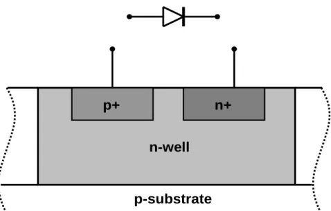
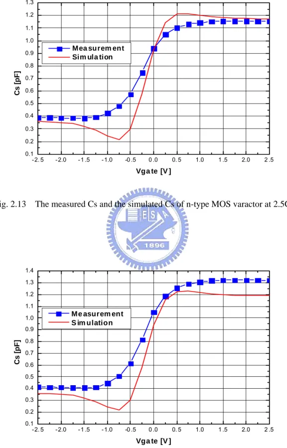
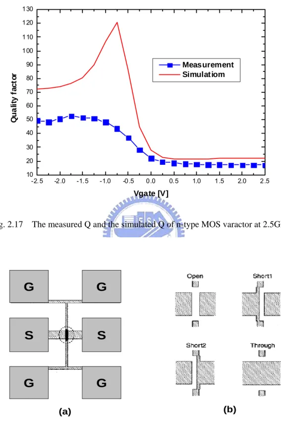
(28) Conversion between Y-parameters and S-parameters is as follows.. Y11 =. (1 − S11 )(1 + S 22 ) + S12 S 21 Y . (1 + S11 )(1 + S 22 ) − S12 S 21 0. (2.3). Y12 =. − 2S12 Y . (1 + S11 )(1 + S 22 ) − S12 S 21 0. (2.4). Y21 =. − 2S 21 Y . (1 + S11 )(1 + S 22 ) − S12 S 21 0. (2.5). Y22 =. (1 + S11 )(1 − S 22 ) + S12 S 21 Y . (1 + S11 )(1 + S 22 ) − S12 S 21 0. (2.6). Y0 is the characteristic admittance.. 2.4.2. Discussion on Pad De-Embedding Methods. The pad de-embedding method used in this thesis is known as Y-parameter subtraction technique, in which the parasitic components in series with the DUT are assumed negligible. Thus, the parasitic components in series with the DUT are not presented in the equivalent circuit of the test structure shown in Fig. 2.10. The complete equivalent circuit of the test structure is shown in Fig. 2.11. The parasitic components in series with the DUT originate from the metal interconnections between the contact pads and the DUT. Y-parameter subtraction technique can de-embed the parasitic components in parallel with the DUT, but it can’t de-embed the parasitic components in series with the DUT. At low frequency, the total impedance of the parasitic components in series with the DUT (not be de-embedded) is much less than that of the DUT. However, for high frequency measurement, the effects of the parasitic components in series with the DUT (not be de-embedded) become significant. Fig. 2.12~Fig. 2.15 shows the measured and simulated C S of n-type MOS varactor at 100MHz, 2.5GHz, 5GHz, and 10GHz respectively. C S is the equivalent series capacitance as described in section 2.5. Of course, the simulated C S is dependent of frequency due to the intrinsic parasitic inductive effect of the DUT (Fig. - 14 -.
(29) 2.16) [7]. Fig. 2.17 shows the measured and simulated Q of n-type MOS varactor at 2.5GHz. All the simulated results are produced by S-parameter simulation in ADS. Due to Y-parameter subtraction technique, it should be noted here that the measured C S and Q contain the effects of the parasitic components in series with the DUT. The difference between the measured results and the simulated results is mainly attributed to the effects of the parasitic components in series with the DUT. The measured C S is strongly different from the simulated C S at 10GHz. However, at 100MHz and 2.5GHz, the difference is much smaller. An advanced pad de-embedding method called three-step de-embedding method [8] [9] can de-embed both the parasitic components in series with the DUT and the parasitic components in parallel with the DUT. The layout of the test structure with the DUT and the corresponding on-wafer de-embedding structures: open, short1, short2, and through, are shown in Fig. 2.18.. 2.5 Equivalent Circuit Model All these four MOS structure varactors are modeled by equivalent series R S − C S circuit between port1 (Vgate ) and port2 (Vcont ) . Using the de-embedded Y-parameters, the impedance between port1 and port2 can be calculated easily at each operating point and frequency as Z =. 1 . Impedance Z can be written as Y11. Z = RS +. 1 . jω C S. (2.7). R S , C S and Q can be extracted as R S = Re(Z) CS = Q=. −1 ω ⋅ Im(Z). Im(Z) 1 = . Re(Z) ωC SR S. 2.6 Measurement Results - 15 -. (2.8) (2.9) (2.10).
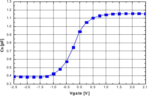
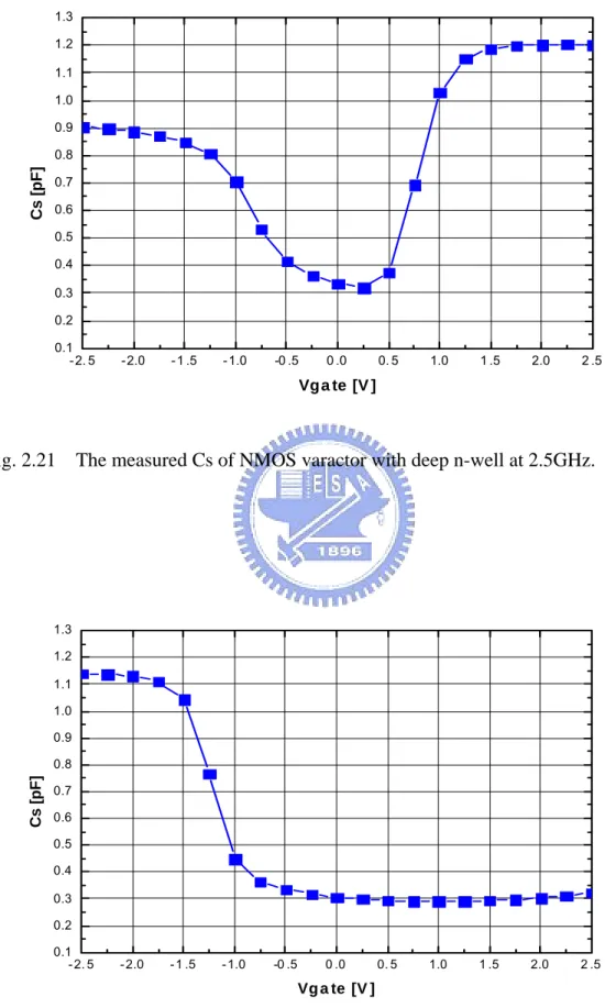
(30) The measured C S of these four MOS structure varactors at 2.5GHz are shown respectively in Fig. 2.19~Fig. 2.22. As shown in section 2.4.2, at low frequency (100MHz, and 2.5GHz), the effects of the parasitic components in series with the DUT (not be de-embedded) result in small difference between the measured C S and the real C S . However, the difference between the measured Q and the real Q is obvious. Therefore, the measured Qs of these four MOS structure varactors don’t make sense and are not shown. The comparison of the measured characteristics among these MOS structure varactors is shown in Table 2.1. As shown in Table 2.1, PMOS varactor has the largest capacitance tuning range and the best area efficiency. Since the signal swings in the VCOs are large, the instantaneous value of C S changes throughout the signal period. The effective capacitance of the varactor is average over each period. It is not sufficient to predict the frequency tuning ranges of the VCOs by considering only the absolute maximum and minimum values of C S . The frequency tuning curves of the VCOs depend on both the signal swings of the VCOs and the capacitance tuning curves of the varactors. For NMOS varactor with deep n-well, the nonmonotonicity of C S shown in Fig. 2.21 will impair the tuning capability of the VCOs.. - 16 -.
(31) p+. n+ n-well. p-substrate. Fig. 2.1. Cross section of p-n junction varactor.. Vgate. Vcont. n+ poly. n+. n+ n-well. p-substrate. Fig. 2.2 Cross section of n-type MOS varactor. - 17 -.
(32) Vgate Vcont. VDD. VDD. p+ poly. n+. p+. n-well. p+. n+. p-well. n-well. deep n-well p-substrate. Fig. 2.3. Cross section of p-type MOS varactor with deep n-well.. Vgate Vcont. VDD. GND. VDD. p+. n+. n+ poly. n+ n-well. n+. n+ p-well. deep n-well p-substrate. Fig. 2.4 Cross section of NMOS varactor with deep n-well. - 18 -. n-well.
(33) Vgate. Vcont. VDD. p+ poly p+. n+. p+. n-well p-substrate. Fig. 2.5. Cross section of PMOS varactor.. Vgate Vgate W. Branch (B). Vcont. (a). L. S: 1 (one side) S: 2 (two side). Group (G). Vcont. (c). (b). Fig. 2.6 The layouts of (a) test structure of n-type MOS varactor, (b) the corresponding de-embedding OPEN structure, and (c) the device. - 19 -.
(34) Vgate Vgate VDD Vcont. (a) VDD. Vcont. (b). (c). Fig. 2.7 The layouts of (a) test structure of p-type MOS varactor with deep n-well, (b) the corresponding de-embedding OPEN structure, and (c) the device.. Vgate GND. Vgate VDD. Vcont. (a). GND. VDD. Vcont. (b). (c). Fig. 2.8 The layouts of (a) test structure of NMOS varactor with deep n-well, (b) the corresponding de-embedding OPEN structure, and (c) the device. - 20 -.
(35) Vgate. Vgate VDD. Vcont. (a). VDD. Vcont. (b). (c). Fig. 2.9 The layouts of (a) test structure of PMOS varactor, (b) the corresponding de-embedding OPEN structure, and (c) the device.. DUT. Fig. 2.10. The parasitic components originating from the contact pads. - 21 -.
(36) Fig. 2.11 The complete equivalent circuit of the RF test structure [8][9].. 1.3 1.2 1.1 1.0. M eas ure me nt S imulat iom. 0.9. Cs [pF]. 0.8 0.7 0.6 0.5 0.4 0.3 0.2 0.1 -2. 5. -2.0. -1 .5. -1.0. -0 .5. 0 .0. 0. 5. 1.0. 1 .5. 2.0. 2 .5. Vga te [V ]. Fig. 2.12 100MHz.. The measured Cs and the simulated Cs of n-type MOS varactor at. - 22 -.
(37) 1.3 1.2 1.1 1.0. Mea surem ent Sim ula tion. 0.9. Cs [pF]. 0.8 0.7 0.6 0.5 0.4 0.3 0.2 0.1 -2. 5. -2.0. -1 .5. -1.0. -0 .5. 0 .0. 0. 5. 1.0. 1 .5. 2.0. 2 .5. Vga te [V ]. Fig. 2.13. The measured Cs and the simulated Cs of n-type MOS varactor at 2.5GHz.. 1.4 1.3 1.2 1.1. Me asurem ent S im ulation. 1.0. Cs [pF]. 0.9 0.8 0.7 0.6 0.5 0.4 0.3 0.2 0.1 -2. 5. -2.0. -1 .5. -1.0. -0 .5. 0 .0. 0. 5. 1.0. 1 .5. 2.0. 2 .5. Vga te [V ]. Fig. 2.14. The measured Cs and the simulated Cs of n-type MOS varactor at 5GHz. - 23 -.
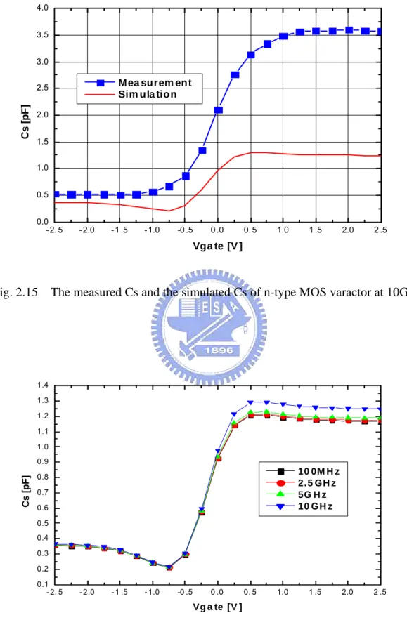
(38) 4.0 3.5 3.0. Mea surem ent Sim ula tion. Cs [pF]. 2.5 2.0 1.5 1.0 0.5 0.0 -2. 5. -2.0. -1 .5. -1.0. -0 .5. 0 .0. 0. 5. 1.0. 1 .5. 2.0. 2 .5. Vga te [V ]. Fig. 2.15. The measured Cs and the simulated Cs of n-type MOS varactor at 10GHz.. 1.4 1.3 1.2 1.1 1.0. Cs [pF]. 0.9. 10 0M H z 2.5 GH z 5G H z 10 GH z. 0.8 0.7 0.6 0.5 0.4 0.3 0.2 0.1 - 2. 5. - 2.0. - 1 .5. - 1.0. -0 .5. 0 .0. 0. 5. 1.0. 1 .5. 2.0. 2 .5. Vg a te [V ]. Fig. 2.16. The simulated Cs of n-type MOS varactor at 100MHz, 2.5GHz, 5GHz,. and 10GHz respectively. - 24 -.
(39) 130 120 110 100. Quality factor. 90. Measurement Simulatiom. 80 70 60 50 40 30 20 10 -2. 5. -2.0. -1. 5. -1.0. -0.5. 0.0. 0. 5. 1.0. 1.5. 2.0. 2.5. Vgate [V]. Fig. 2.17. The measured Q and the simulated Q of n-type MOS varactor at 2.5GHz.. G. G. S. S. G. G (b). (a). Fig. 2.18. (a) The layout of the test structure with the DUT. (b) Magnified view of. the layout of the de-embedding structures. The pad layout and interconnection layout are equal to the test structure. - 25 -.
(40) 1.3 1.2 1.1 1.0. Cs [pF]. 0.9 0.8 0.7 0.6 0.5 0.4 0.3 - 2. 5. - 2.0. - 1 .5. - 1.0. -0 .5. 0 .0. 0. 5. 1.0. 1 .5. 2.0. 2 .5. Vg a te [V ]. Fig. 2.19. The measured Cs of n-type MOS varactor at 2.5GHz.. 1.3 1.2 1.1 1.0 0.9. Cs [pF]. 0.8 0.7 0.6 0.5 0.4 0.3 0.2 0.1 - 2. 5. - 2.0. -1 .5. -1.0. -0 .5. 0.0. 0 .5. 1. 0. 1 .5. 2 .0. 2.5. V gate [ V]. Fig. 2.20. The measured Cs of p-type MOS varactor with deep n-well at 2.5GHz. - 26 -.
(41) 1.3 1.2 1.1 1.0 0.9. Cs [pF]. 0.8 0.7 0.6 0.5 0.4 0.3 0.2 0.1 - 2. 5. -2.0. -1 .5. -1.0. -0 .5. 0 .0. 0. 5. 1.0. 1 .5. 2.0. 2 .5. Vga te [V ]. Fig. 2.21. The measured Cs of NMOS varactor with deep n-well at 2.5GHz.. 1.3 1.2 1.1 1.0 0.9. Cs [pF]. 0.8 0.7 0.6 0.5 0.4 0.3 0.2 0.1 - 2. 5. - 2.0. - 1 .5. - 1.0. -0 .5. 0 .0. 0. 5. 1.0. Vg a te [V ]. Fig. 2.22. The measured Cs of PMOS varactor at 2.5GHz. - 27 -. 1 .5. 2.0. 2 .5.
(42) Table 2.1 The comparison of the measured characteristics of different MOS structure varactors. C s, min (pF) C s, max (pF). C s, max C s, min. well area ( um 2 ). n-type MOS varactor. 0.3853. 1.156. 3. 1121.2203. p-type MOS varactor with deep n-well. 0.3403. 1.134. 3.33. 1937.5403. NMOS varactor with deep n-well. 0.3206. 1.203. 3.75. 1937.5403. PMOS varactor. 0.2914. 1.139. 3.91. 1121.3604. - 28 -.
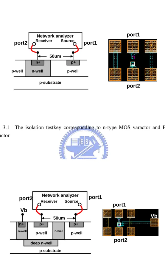
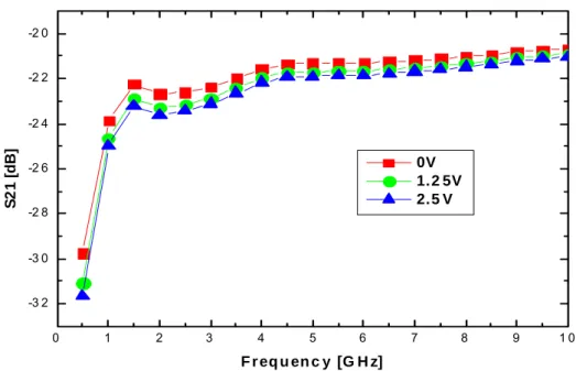
(43) Chapter 3 Substrate Noise Isolation Test. 3.1 The Structures of Testkeys All the MOS structure varactors mentioned in chapter 2 are placed in separate wells to isolate substrate noise. N-type MOS varactor and PMOS varactor fabricated on n-well use the p-n junction between n-well and substrate to isolate substrate noise. P-type MOS varactor with deep n-well and NMOS varactor with deep n-well are fabricated on p-well and surrounded by deep n-well and n-well in order to isolate substrate noise. An experiment is designed to compare the isolation capability of these two structures. The isolation testkey corresponding to n-type MOS varactor and PMOS varactor is show in Fig. 3.1. The isolation testkey corresponding to NMOS varactor with deep n-well and p-type MOS varactor with deep n-well is show in Fig. 3.2. The source window and the receiver window are 20um x 20um p+ or n+ region connected to GSG pads by metal. The space between the source window and the receiver window is 50um. These two testkeys are realized in a 0.25-um CMOS process.. 3.2 Measurement Results The measured S 21 parameters of the testkey shown in Fig. 3.1 are shown in Fig. 3.3. The n-well is biased at 0V, 1.25V, and 2.5V respectively. The measured S 21 parameters of the testkey shown in Fig. 3.2 are shown in Fig. 3.4. The deep n-well is biased at 0V, 1.25V, 2.5V, and floating respectively. The isolation capability is determined by the value of the p-n junction capacitance between n-well and substrate. At higher frequency, it is more difficult to isolate substrate noise by p-n junction - 29 -.
(44) between n-well and substrate, as shown in Figs. 3.3, and 3.4. Thus, the larger the voltage difference between n-well and substrate, the better the isolation capability is. The comparisons of the isolation capability of different isolation structures are presented in Fig. 3.5 and Fig. 3.6. At low frequency (<1GHz), the isolation structure shown in Fig. 3.2 has better isolation capability. However, these two isolation structures have almost equal isolation capability from 1GHz to 10GHz.. - 30 -.
(45) port1. Network analyzer Receiver. port2. Source. port1. 50um p-well. n+. p+. n-well. p-well. p-substrate. port2. Fig. 3.1 The isolation testkey corresponding to n-type MOS varactor and PMOS varactor. port2. Network analyzer Receiver. port1. Source. port1. Vb Vb. 50um n+. p+. n-well. p-well. p+ n-well. p-well. port2. deep n-well p-substrate. Fig. 3.2 The isolation testkey corresponding to p-type MOS varactor with deep n-well and NMOS varactor with deep n-well. - 31 -.
(46) -2 0 -2 2. S21 [dB]. -2 4. 0V 1.2 5V 2.5 V. -2 6 -2 8. -3 0 -3 2 0. 1. 2. 3. 4. 5. 6. 7. 8. 9. 10. F r eq u en c y [G H z]. Fig. 3.3. The measured S 21 parameters of the testkey shown in Fig. 3.1. The n-well. is biased at 0V, 1.25V, and 2.5V respectively.. -2 0 -2 2 -2 4. flo atin g 0V 1.25 V 2.5V. S21 [dB]. -2 6 -2 8 -3 0 -3 2 -3 4 -3 6. 0. 1. 2. 3. 4. 5. 6. 7. 8. 9. 10. F r eq u en c y [G H z]. Fig. 3.4. The measured S 21 parameters of the testkey shown in Fig. 3.2. The deep. n-well is biased at 0V, 1.25V, 2.5V, and floating respectively. - 32 -.
(47) -2 0 -2 2 -2 4. S21 [dB]. -2 6. n -w ell=0 V d ee p n- we ll= 2.5V. -2 8 -3 0 -3 2 -3 4 -3 6. 0. 1. 2. 3. 4. 5. 6. 7. 8. 9. 10. F r eq u en c y [G H z]. Fig. 3.5. The comparison of the isolation capability of different isolation structures.. The n-well in Fig. 3.1 is biased at 0V. The deep n-well in Fig. 3.2 is biased at 2.5V.. -2 0 -2 2 -2 4. S21 [dB]. -2 6 -2 8. n -w ell= 2 .5 V d ee p n -w ell= 2.5V. -3 0 -3 2 -3 4 -3 6. 0. 1. 2. 3. 4. 5. 6. 7. 8. 9. 10. F req u en c y [G H z]. Fig. 3.6 The comparison of the isolation capability of different isolation structures. The n-well in Fig. 3.1 is biased at 2.5V. The deep n-well in Fig. 3.2 is biased at 2.5V. - 33 -.
(48) Chapter 4 Design Considerations for LC-tank VCOs. 4.1 LC-tank VCO Basics Oscillators utilized in RF applications often fall in the feedback category (Fig. 4.1), but, where applicable, the one-port model can give additional insight into their operation. The “one-port model” treats the oscillator as two one-port networks connected to each other, as shown in Fig. 4.2(a). To understand this model, suppose the resonator is a simple tank, as shown in Fig. 4.2(b) along with its parasitic resistances. For a narrow band of frequencies, the circuit can be converted to the parallel combination depicted in Fig. 4.2(c). The tank by itself does not oscillate indefinitely because some of the stored energy is dissipated in R P in every cycle. The idea in the one-port model is that an active network generates an impedance equal to − R P so that the equivalent parallel resistance seen by the intrinsic, lossless resonator is infinite. In essence, the energy lost in R P is replenished by the active circuit in every cycle, allowing steady oscillation [10]. As the capacitor C in Fig. 4.2(c) is proportional to a tuning input voltage, the circuit results in a VCO with center frequency f0 =. 1 2π LC. .. (4.1). The capacitor C in Fig. 4.2(c) not only consists of a variable capacitor to tune the oscillator, but it also includes the parasitic or fixed capacitances of the inductor, the active elements, and the load (output driver, mixer, prescaler, etc.). The self-sustaining effect allows the circuit’s noise to grow initially, but another mechanism is necessary to limit the growth at some point. To ensure oscillation start-up, the small-signal loop - 34 -.
(49) gain must be somewhat greater than one, but to achieve stable amplitude, the “average” loop gain must return to unity.. 4.2 Phase Noise 4.2.1. Definition. As other analog circuits, oscillators are susceptible to noise. Noise injected into an oscillator by its constituent devices or by external means may influence both the frequency and the amplitude of the output signal. In most cases, the disturbance in the amplitude is negligible or unimportant, and only the random deviation of the frequency is considered. In RF applications, phase noise is usually characterized in the frequency domain. For an ideal sinusoidal oscillator operating at ω 0 , the spectrum assumes the shape of an impulse, whereas for an actual oscillator, the spectrum exhibits “skirts” around the carrier frequency ω 0 , as shown in Fig. 4.3. To quantify phase noise, we consider a unit bandwidth at an offset ∆ω with respect to ω 0 , calculate the noise power in this bandwidth, and divide the result by the carrier (average) power.. ⎡P (ω + ∆ω,1Hz)⎤ L{∆ω} = 10 ⋅ log⎢ sideband 0 ⎥, Pcarrier ⎣ ⎦. (4.2). where Psideband (ω 0 + ∆ω,1Hz ) represents the single sideband power at a frequency offset of ∆ω from the carrier with a measurement bandwidth of 1Hz.. 4.2.2. Conversion of Noise to Phase Noise. Oscillator phase noise is generated primarily through two mechanisms, distinguished by the path into which the noise is injected. Illustrated in Fig. 4.4, the noise, x(t) , appearing in these paths gives rise to distinctly different effects.. 4.2.2.1 Noise Mixing and Noise Folding - 35 -.
(50) If we treat VCO as a linear time-invariant (LTI) system, the noise injected into the signal path [Fig. 4.4(a)] simply mixes with the carrier (Fig. 4.5). Oscillators usually experience amplitude limiting and hence nonlinearity, thus “folding” the noise components. If the open-loop input/output characteristic of VCO 2. is expressed as Vout = α1Vin + α 2 Vin + α 3 Vin , then for an input consisting of the 3. carrier and a noise component, e.g., Vin (t ) = A 0 cosω 0 t + A n cosω n t , the output exhibits the following important terms: Vout1 (t ) ∝ α 2 A 0 A n cos(ω 0 ± ω n )t. (4.3). Vout2 (t ) ∝ α 3 A 0 A n2 cos(ω 0 − 2ω n )t. (4.4). Vout3 (t ) ∝ α 3 A 02 A n cos(2ω 0 − ω n )t .. (4.5). Note that Vout1 (t ) appears in band if ω n is small. However, in a fully differential configuration usually used, Vout1 (t ) = 0 because α 2 = 0 . Also, Vout2 (t ) is negligible because A n ⟨⟨ A 0 . Therefore, Vout3 (t ) is the only significant cross-product. Thus, the nonlinearity folds all the noise components below ω 0 to the region above and vice versa. Such components are significant if they are close to ω 0 . This phenomenon is illustrated in Fig. 4.6. This simplified analysis predicts the frequency of the components in response to injected noise, but not their magnitude. When noise is injected into the signal path of VCO, the magnitude of the observed response at ω n and 2ω 0 − ω n depends on the noise shaping property of the VCO [11].. 4.2.2.2 Frequency Modulation When the noise is injected into the control path [Fig. 4.4(b)], viewed as analog frequency modulation, this effect translates the noise in the control path to the region around the carrier, as described as follows. Frequency is defined as the derivative of phase with respect to time: - 36 -.
(51) ω = dφ / dt.. (4.6). Equation (4.5) indicates that, if the frequency of a waveform is known as a function of time, the phase can be computed as φ = ∫ ωdt + φ 0 .. (4.7). Let’s use K VCO to denote the VCO gain and Vcont to denote the control voltage. In particular, since for a VCO, ω out = ω 0 + K VCO × Vcont , we have Vout (t) = V0 cos( ∫ ω out dt + φ 0 ) = V0 cos(ω 0 t + K VCO ∫ Vcont dt + φ 0 ) .. (4.8). The initial phase φ0 is usually unimportant and is assumed zero hereafter. When a VCO sense a small sinusoidal control voltage Vcont = Vn cosω n t , the output is expressed as Vout (t) = V0 cos(ω 0 t + K VCO ∫ Vcont dt ). = V0 cos(ω 0 t + K VCO. Vn sinω n t) ωn. = V0 cosω 0 tcos(K VCO. (4.9) (4.10). Vn sinω n t) ωn. − V0 sinω 0 tsin(K VCO. Vn sinω n t) ωn. (4.11). If Vn is small enough that K VCO Vn /ω n ⟨⟨1radius, then. Vout (t) ≈ V0 cosω 0 t − V0 (sinω 0 t)(K VCO. Vn sinω n t) ωn. (4.12). = V0 cosω 0 t. −. K VCO Vn V0 [cos(ω 0 − ω n )t − cos(ω 0 + ω n )t] . 2ω n. (4.13). The output consists of three sinusoidal having frequencies of ω 0 , ω 0 − ω n , and ω 0 + ω n . The spectrum is shown in Fig. 4.7. The components at ω 0 ± ω n are called “sidebands” [12]. In practice, K VCO is proportional to the carrier frequency because for a given - 37 -.
(52) control voltage range, the tuning range must be a constant percentage of the center frequency so as to compensate for process and temperature variations. This effect makes flicker noise (low-frequency noise) in the control path particularly detrimental. Called flicker noise upconversion, this phenomenon deteriorates the phase noise at low offset from the carrier. As we have seen, the MOS structure varactors allow a high tuning range in a small control voltage range. This is highly desirable for designs of the scaled technologies. On the other hand, the VCO gain can become excessively high, especially for high operation frequency band. This can constitute a problem because of the high sensitivity of the MOS structure varactors to the control voltage. The bandswitching topology is suggested to decrease the sensitivity of the varactor [13], and hence, the low-frequency noise upconversion is reduced.. 4.2.3. Phase noise model. The semi-empirical model reported in [14]-[16], known also as the Leeson-Cutler phase noise model, is based on an LTI assumption for tuned tank oscillators. It predicts the following behavior for L{∆ω}: 2 ⎧⎪ 2FkT ⎡ ⎛ ω ∆ω1/f 3 ⎞ ⎤ ⎛ 0 ⎟⎟ ⎥ ⋅ ⎜1 + ⋅ ⎢1 + ⎜⎜ L{∆ω} = 10 ⋅ log⎨ ⎜ ∆ω ⎪⎩ p s ⎢⎣ ⎝ 2Q L ∆ω ⎠ ⎥⎦ ⎝. ⎞⎫⎪ ⎟⎬ ⎟ ⎠⎪⎭. (4.14). where F is an empirical parameter (often called the “device excess noise number”), k is Boltzmann’s constant, T is the absolute temperature, Ps is the average power dissipated in the resistive part of the tank, ω 0 is the oscillation frequency, Q L is the effective quality factor of the tank with all the loadings in place (also known as loaded Q), ∆ω is the offset from the carrier and ∆ω1/f 3 is the frequency of the corner between the 1/f 3 and 1/f 2 regions, as shown in the sideband spectrum of Fig. 4.8 [17]. - 38 -.
(53) 4.3 LC-tank VCO Topologies Cross-coupled NMOS and PMOS transistors can provide negative resistance to compensate the losses in the tank. Fig. 4.9 shows three types of LC-tank VCO topology. The tail current sources are omitted because they are an important flicker-noise source. The upconversion of flicker noise to 1/f 3 phase noise is an important issue in LC-tank VCOs. In the topologies with tail current sources, the cross-coupled NMOS and PMOS transistors are expected to feature lower flicker noise than the tail transistors for two main reasons. First, the cross-coupled NMOS and PMOS transistors operate in triode region for large portions of the oscillation period; hence, they exhibit lower current flicker noise than the tail transistors that continuously operate in saturation. Second, switched MOS transistors are known to have lower flicker noise than transistors biased in the stationary condition [18]. In other words, tail current sources dominate 1/f 3 phase noise. Thus, from the phase-noise point of view, the topologies without tail current sources are expected to show better phase-noise performance than those with tail current sources. The main drawback often attributed to the topologies without tail current sources is a higher sensitivity of the frequency to the supply voltage (frequency pushing). This effect can be reduced by using a supply voltage regulator [19]. Compared to NMOS-only topology and PMOS-only topology, complementary topology has less power consumption, as current is reused. However, complementary topology uses more transistors (4 transistors) to realize negative resistance and thus results in more noise sources, compared to NMOS-only topology (2 transistors) and PMOS-only topology (2 transistors). Furthermore, PMOS transistors inherently show lower flicker noise (approximately 10 dB), compared to NMOS transistors. Thus,. - 39 -.
(54) among these three types of topology, PMOS-only topology is expected to have the best phase-noise performance. Apart from the advantage mentioned above, two additional advantages in using PMOS-only topology are list below: (1) The inductors force the average value of the outputs to ground and no modulation of the varactor bias point is induced by the supply voltage. Therefore, frequency pushing is reduced. (2) Being inside an n-well, the PMOS transistor is less susceptible to substrate coupling noise pickup than the NMOS transistor.. 4.4 Output Buffer The placement of a 50-ohm load directly at the terminals of the tank such as when testing with a spectrum analyzer would reduce the Q of the circuits and influence the oscillation frequency. For this reason, output buffers must be added to the circuits. Too small transistor can not provide enough output current drive. However, the gate oxide capacitance and parasitic capacitances of the transistors used as output buffers will lower oscillation frequency and reduce frequency tuning range. The outputs can be buffered by using source followers for measurement purposes. The current sources of the source followers are replaced with external Bias Tees to provide high ac impedance. In this way, small transistors can be used to provide enough output current drive without loading the VCO core excessively [20]. However, linearity is the main consideration for output buffers. Thus, the common source configuration is better than the source follower configuration because the body effect of the source follower is damaged to the circuit linearity. At high frequency, active devices present more serious nonlinearity due to nonlinear parasitic. Thus, active load is replaced with passive load (inductor). The dc feed inductor force the. - 40 -.
(55) drain voltage of output buffer to VDD . Therefore, the bias point of output buffer is less susceptible to process variation and temperature variation.. - 41 -.
(56) +. X (s). +. Y (s). H (s). +. Frequency selective network. Fig. 4.1 Feedback oscillatory system with frequency-selective network.. R1 R 2 Active Circuit. C. L. Rp. C. L. Resonator. R 1 = −R 2. (a). Fig. 4.2 of (b).. (b). (c). (a) One port view of oscillators, (b) LC resonator, and (c) equivalent circuit. - 42 -.
(57) Ideal Oscillator. ω0. Fig. 4.3. Actual Oscillator. ω0 ∆ω. ω. ω. Output spectrum of ideal and actual oscillators.. Vcont Vcont Noise x(t) + + +. H (s). Noise y(t). (a). Fig. 4.4. + H (s). (b). Phase noise in (a) signal path, and (b) control path. - 43 -. Vout.
(58) Y X. Noise Power Spectral Density. Output Spectrum. 2. X. ω0. ω. ω0. ω. ω0. ω. Fig. 4.5 Noise shaping in oscillators.. + ω0 ωn. Fig. 4.6. H (s). ω. 2ω 0 − ω n ω n. Noise folding in an oscillator. - 44 -.
(59) Vcont − ωn. 0. ωn. VCO. ω ω 0 − ωn. ω0. ω ω0 + ωn. Fig. 4.7 Modulation of VCO frequency by noise on control line.. L (∆ω ). -3. -2 ⎛ 2FkT 10 ⋅ log⎜⎜ ⎝ Ps. ∆ω 1/f 3. Fig. 4.8. ω0 2Q. log (∆ω ). Phase noise spectrum according to Leeson-Cutler phase noise model. - 45 -. ⎞ ⎟⎟ ⎠.
(60) 1/2 V DD, max. 1/2 V DD, max. VDD, max. V cont. V cont. (b). (c). V cont. (a). Fig. 4.9 (a) PMOS-only topology, (b) NMOS-only topology, and (c) complementary topology.. - 46 -.
(61) Chapter 5 Circuit Designs and Implementation. 5.1 Circuit Designs Three 2.4GHz LC VCOs (VCO1, VCO2, and VCO3) are realized in a 0.25-um CMOS process for comparison. The topology of VCO1 and VCO2 with output buffers is shown in Fig. 5.1 (PMOS-only topology). VCO1 and VCO2 differ only in the type of varactor: n-type MOS varactor (VCO1) and NMOS varactor with deep n-well (VCO2). Their sizes are equal (L x W x S x B x G=1um x 5um x 1 x 6 x 6). Each side of the control voltage node has two varactors in parallel. The top view of the spiral inductor used is shown in Fig. 5.2 with key design parameters. The key design parameters are depicted in the following: N: number of the coil turn, which is 2.5 in Fig. 5.2. W: width of the top metal, which is 10um in Fig. 5.2. S: space of top metal, which is 2um in Fig. 5.2. R: radius of inner coil, which is 60um in Fig. 5.2. The size of the cross-coupled PMOS transistors is 0.24um x 5um x 24 (L x W x Finger). The open-drain PMOS transistors are used as output buffers. Power supply provides bias voltages for the open-drain PMOS transistors with the use of external Bias Tees. The size of the open-drain PMOS transistors is also 0.24um x 5um x 24 (L x W x Finger). In VCO1 and VCO2, the RF signal injected into the substrate as substrate noise is provided by signal generator. The RF signal is injected into the substrate through the p+ ring surrounding the varactors. In this thesis, we focus on the influences of. - 47 -.
(62) substrate noise coupling to the varactors on the output spectrums of VCO1 and VCO2. Thus, the varactors and the surrounding p+ ring are placed apart from the rest of the circuit. Furthermore, in order to prevent the injected substrate noise from coupling to the cross-coupled PMOS transistors, the cross-coupled PMOS transistors are surrounded by another p+ guard ring. The arrangement described above is shown in Fig. 5.3. In order to facilitate comprehension, the topology shown in Fig. 5.1 is redrawn to the combination of a feedback loop, varactors, and output buffers. An additional 2.4GHz VCO circuit (VCO3) adopting complementary topology is designed (Fig. 5.4). The type of varactor is n-type MOS varactor. Each side of the control voltage node has single varactor (L x W x S x B x G=1um x 5um x 1 x 6 x 6). The core spiral inductor is the same as that used in VCO1 and VCO2. The size of the cross-coupled NMOS transistors is 0.24um x 5um x 8 (L x W x Finger). The size of the cross-coupled PMOS transistors is 0.24um x 5um x 24 (L x W x Finger). The open-drain NMOS transistors (L x W x Finger=0.24um x 5um x 8) are used as output buffers. As mentioned in section 4.3, PMOS-only topology is expected to have lower phase noise than complementary topology. Therefore, VCO3 is designed to compare with VCO1.. 5.2 Simulation Results For comparison reason, the structure and layout of NMOS with deep n-well used as varactor in VCO2 is different from that of NMOS with deep n-well used as transistor in the given 0.25um CMOS process. Therefore, there is no model for simulation. The simulated results of VCO1 and VCO3 are summarized in Table 5.1 and Table 5.3 respectively. It should be noted that the simulated phase noise of VCO1 is lower than that of VCO3. The simulation tool is Agilent Advance Design System.. 5.3 Layout Designs - 48 -.
(63) Fig. 5.5 shows the layout of VCO1. The total area is 1110um x 1000um. The arrangement of the component devices is spiral inductors, all transistors, and varactors respectively from the top to the bottom of the layout. The symmetry of the layout is well considered. In order to conform the specific layout rules of the on-wafer measurement in National Nano Device Laboratories (NDL), the RF GSG pads of output signals are arranged on left and right side, the RF GSG pads of input signal used as substrate noise are arranged on top side, the PGPPGP DC pads are arranged on bottom side, and the single DC pad on top side is connected to the ground node of the spiral inductors. Fig. 5.6 shows the layout of VCO2. The total area is 1110um x 1000um. The arrangement of the layout is similar to that of VCO1. Fig. 5.7 shows the layout of VCO3. The total area is 1110um x 1000um. The arrangement of the component devices is spiral inductors, all transistors, and varactors respectively from the top to the bottom of the layout. The symmetry of the layout is well considered. In order to conform the specific layout rules of the on-wafer measurement in National Nano Device Laboratories (NDL), the RF GSG pads of output signals are arranged on left and right side, and the PGPPGP DC pads are arranged on bottom side.. 5.4 Measurement Results The output spectrums and the phase noise of the VCO circuits are measured using Agilent E4407B spectrum analyzer. The RF signal injected into the substrate as substrate noise is provided by signal generator. Fig. 5.8 shows the measured output spectrum of VCO1 at 1.9358-GHz oscillation frequency. Fig. 5.9 shows the measured and simulated oscillation frequency of VCO1 versus the control voltage Vcont . Fig. 5.10 shows the measured. - 49 -.
(64) phase noise of VCO1 at 1.9368-GHz carrier frequency. The phase noise at 1-MHz offset from the carrier is -93.39dBc/Hz. The phase noise at 100-KHz offset from the carrier is estimated at about -70dBc/Hz according to Fig. 5.10. Fig. 5.11 shows the measured output spectrum of VCO2 at 2.548-GHz oscillation frequency. Fig. 5.12 shows the measured oscillation frequency of VCO2 versus the control voltage Vcont . Fig. 5.13 shows the measured phase noise of VCO2 at 2.5493-GHz carrier frequency. The phase noise at 1-MHz offset from the carrier is -98.56dBc/Hz. The phase noise at 100-KHz offset from the carrier is estimated at about -85dBc/Hz according to Fig. 5.13. Fig. 5.14 shows the measured output spectrum of VCO3 at 2.2327-GHz oscillation frequency. Fig. 5.15 shows the measured and simulated oscillation frequency of VCO3 versus the control voltage Vcont . Fig. 5.16 shows the measured phase noise of VCO3 at 2.4333-GHz carrier frequency. The phase noise at 1-MHz offset from the carrier is -102.82dBc/Hz. The phase noise at 100-KHz offset from the carrier is estimated at about -80dBc/Hz according to Fig. 5.16. The measured and simulated results of VCO1, VCO2, and VCO3 are summarized in Table 5.1, Table 5.2, and Table 5.3, respectively. It should be noted that the measured phase noise is much higher than the simulated phase noise. This problem is attributed to the extra noise on DC pads generating by current switching through the parasitics of DC probes. However, the DC voltage sources in the simulator are ideal and noiseless. Thus, the extra noise on DC pads deteriorates the measured phase noise. The parasitics of DC probes also results in the shift of the measured oscillation frequency from the simulated oscillation frequency. This problem can be improved by adding bypass capacitors between DC pads and ground pads in the layouts. As shown in Table 5.1 and Table 5.3, the simulated phase noise of VCO1 is lower than that of VCO3 because VCO1 has fewer constituent devices and - 50 -.
(65) thus less noise source. However, the measured phase noise of VCO1 is higher than that of VCO3. This problem is attributed to the higher VCO gain of VCO1. The higher VCO gain makes VCO1 more sensitive to the extra noise on DC pads. Table 5.1 shows that the frequency tuning range of VCO1 is 548MHz, at 1.3-V control voltage range. Table 5.3 shows that the frequency tuning range of VCO3 is 505MHz, at 2.5-V control voltage range. In VCO1, at 2.499-GHz oscillation frequency, the measured output spectrum without substrate noise injection and the measured output spectrum with substrate noise injection are shown in Fig. 5.17. In VCO2, at 2.5713-GHz oscillation frequency when the deep n-wells of NMOS varactors are biased at 2.5V, the measured output spectrum without substrate noise injection and the measured output spectrum with substrate noise injection are shown in Fig. 5.18. At 2.5692-GHz oscillation frequency when the deep n-wells of NMOS varactors are biased at 0V, the measured output spectrum without substrate noise injection and the measured output spectrum with substrate noise injection are shown in Fig. 5.19. At 2.5686-GHz oscillation frequency when the deep n-wells of NMOS varactors are floating, the measured output spectrum without substrate noise injection and the measured output spectrum with substrate noise injection are shown in Fig. 5.20. It is noted here that the oscillation frequency shifts when the deep n-wells are biased at different conditions (without substrate noise injection). Therefore, the shift of oscillation frequency doesn’t result from substrate noise injection. When power supply is off, the measured output spectrum with substrate noise injection is shown in Fig. 5.21. This shows that the injected substrate noise travels through the substrate and then couples to the output pads. A 2.6-GHz signal with 0-dBm power provided by signal generator is injected into the substrate as substrate noise. It is obvious that “noise folding” happens when - 51 -.
(66) substrate noise is injected. As mentioned in section 4.2.2, the magnitudes of the components at ω n and 2ω 0 − ω n depends on the noise shaping properties of VCO circuits. Noise shaping property is relative to the quality factor of LC tank. VCO1 and VCO2 differ in the type of varactor. Thus, they have different noise shaping properties. In VCO2, the magnitudes of the components at 2ω 0 − ω n in Figs. 5.18, 5.19, and 5.20 are almost equal. This shows that different bias conditions of the deep n-wells have little influence on the magnitudes of the components at ω n and 2ω 0 − ω n . As shown in Fig. 3.4, deep n-well biased at 2.5V has best isolation capability, and floating deep n-well has worst isolation capability. However, the difference of their measured S 21 is small at high frequency (>1GHz).. - 52 -.
(67) V =1.25V DD Mp. Bias Tee. Mp. Mp. var. Mp. Bias Tee. var. V cont. LO+ Ls. LOLs On-chip. V = GND b. Fig. 5.1. V = GND b. The circuit topology of VCO1 and VCO2.. Fig. 5.2 The top view and physical dimension of spiral inductor. - 53 -.
(68) p+ ring. RF signal. Vcont. VDD. VDD. VDD. VDD. GND. p+ guard ring Fig. 5.3 The circuit topology of VCO1 and VCO2 with substrate noise injection, and the Bias Tees are not drawn.. Bias Tee. V = 2.5V DD. V = 2.5V b Mp. cont. var. Mn. Bias Tee. Mp. V LO+. V = 2.5V b. var. Ls. LO-. Mn. Ls. Mn. Mn On-chip. Fig. 5.4. The circuit topology of VCO3. - 54 -.
(69) RF signal. GND. spiral inductors GND. GND. Bias Tee. Bias Tee. LO+. LO-. transistors n-type MOS varactors. Fig. 5.5. VDD. Vcont GND VDD. The layout of VCO1.. spiral inductors. GND. RF signal. GND. GND. Bias Tee. Bias Tee. LO+. LO-. transistors NMOS varactors VDD GND VDD Vcont VDD GND with deep n-well. Fig. 5.6. The layout of VCO2. - 55 -.
(70) spiral inductors. LO+. VDD. VDD. Bias Tee. Bias Tee. LO-. transistors n-type MOS varactors. Fig. 5.7. GND. Vcont. GND VDD. The layout of VCO3.. Fig. 5.8 The measured output spectrum of VCO1 at 1.9358-GHz oscillation frequency. - 56 -.
(71) 2.7. Oscillation frequency [GHz]. 2.6 2.5 2.4 2.3. Measurement Simulation. 2.2 2.1 2.0 1.9 0.0. 0.1. 0. 2. 0.3. 0.4. 0.5. 0.6. 0.7. 0.8. 0.9. 1.0. 1.1. 1.2. 1.3. Vcont [V]. Fig. 5.9 The measured and simulated oscillation frequency of VCO1 versus the control voltage Vcont .. Fig. 5.10. The measured phase noise of VCO1 at 1.9368-GHz carrier frequency. - 57 -.
(72) Fig. 5.11 The measured output spectrum of VCO2 at 2.548-GHz oscillation frequency.. 2.63. Oscillation frequency [GHz]. 2.62 2.61 2.60 2.59 2.58 2.57 2.56 2.55 2.54 0.0. 0.1. 0.2. 0.3. 0.4. 0.5. 0.6. 0.7. 0.8. 0.9. 1.0. 1.1. 1.2. 1.3. Vcont [V]. Fig. 5.12 The measured oscillation frequency of VCO2 versus the control voltage Vcont . - 58 -.
(73) Fig. 5.13. The measured phase noise of VCO2 at 2.5493-GHz carrier frequency.. Fig. 5.14 The measured output spectrum of VCO3 at 2.2327-GHz oscillation frequency. - 59 -.
(74) 2.9. Oscillation frequency [GHz]. 2.8. Measurement Simulation. 2.7 2.6 2.5 2.4 2.3 2.2 0.0. 0.5. 1.0. 1.5. 2.0. 2.5. Vcont [V]. Fig. 5.15 The measured and simulated oscillation frequency of VCO3 versus the control voltage Vcont .. Fig. 5.16. The measured phase noise of VCO3 at 2.4333-GHz carrier frequency. - 60 -.
(75) -1.683dBm. 2.499GHz (fo). (a). -1.723dBm. -22.57dBm -49.23dBm. 2.398GHz (2fo-fn). 2.499GHz (fo). 2.6GHz (fn). (b) Fig. 5.17 In VCO1, at 2.499-GHz oscillation frequency, (a) the measured output spectrum without substrate noise injection and (b) the measured output spectrum with substrate noise injection. - 61 -.
(76) -2.817dBm. 2.5713GHz (fo). (a). -2.97dBm -21.69dBm -32.28dBm. 2.543GHz (2fo-fn). 2.5713GHz (fo). 2.6GHz (fn). (b) Fig. 5.18 In VCO2, at 2.5713-GHz oscillation frequency when the deep n-wells of NMOS varactors are biased at 2.5V, (a) the measured output spectrum without substrate noise injection and (b) the measured output spectrum with substrate noise injection. - 62 -.
(77) -2.741dBm. 2.5692GHz (fo). (a). -2.61dBm -21.01dBm -33.28dBm. 2.5382GHz (2fo-fn). 2.5692GHz (fo). 2.6GHz (fn). (b) Fig. 5.19 In VCO2, at 2.5692-GHz oscillation frequency when the deep n-wells of NMOS varactors are biased at 0V, (a) the measured output spectrum without substrate noise injection and (b) the measured output spectrum with substrate noise injection. - 63 -.
(78) -2.785dBm. 2.5686GHz (fo). (a). -2.72dBm -21.75dBm -33.68dBm. 2.5371GHz (2fo-fn). 2.5686GHz (fo). 2.6GHz (fn). (b) Fig. 5.20 In VCO2, at 2.5686-GHz oscillation frequency when the deep n-wells of NMOS varactors are floating, (a) the measured output spectrum without substrate noise injection and (b) the measured output spectrum with substrate noise injection. - 64 -.
(79) -22.63dBm. 2.6GHz. Fig. 5.21 In VCO2, when power supply is off, the measured output spectrum with substrate noise injection.. Table 5.1 A summary of the measured and simulated results of VCO1.(*estimated) Simulation. Measurement. Power supply. 1.25V. 1.25V. Control voltage. 0~1.3V. 0~1.3V. Frequency range. 2.187~2.706GHz. 1.936~2.484GHz. Tuning range. 519MHz. 548MHz. Phase noise@100KHz. -106.86dBc/Hz. * -70dBc/Hz. Phase noise@1MHz. -126.86dBc/Hz. -93.39dBc/Hz. VCO bias current. 9mA. 11mA. - 65 -.
(80) Table 5.2 A summary of the measured results of VCO2.(*estimated) Measurement Power supply. 1.25V. Control voltage. 0~1.3V. Frequency range. 2.548~2.615GHz. Tuning range. 67MHz. Phase noise@100KHz. *-85dBc/Hz. Phase noise@1MHz. -98.56dBc/Hz. VCO bias current. 11mA. Table 5.3 A summary of the measured and simulated results of VCO3.(*estimated) Simulation. Measurement. Power supply. 2.5V. 2.5V. Control voltage. 0~2.5V. 0~2.5V. Frequency range. 2.242~2.84GHz. 2.233~2.738GHz. Tuning range. 598MHz. 505MHz. Phase noise@100KHz. -93.24dBc/Hz. * -80dBc/Hz. Phase noise@1MHz. -120.66dBc/Hz. -102.82dBc/Hz. VCO bias current. 8mA. 8mA. - 66 -.
數據

![Fig. 2.11 The complete equivalent circuit of the RF test structure [8][9]. -2. 5 -2.0 -1 .5 -1.0 -0 .5 0 .0 0](https://thumb-ap.123doks.com/thumbv2/9libinfo/8223800.170652/36.892.157.740.158.530/fig-complete-equivalent-circuit-rf-test-structure.webp)
+7
相關文件
When we know that a relation R is a partial order on a set A, we can eliminate the loops at the vertices of its digraph .Since R is also transitive , having the edges (1, 2) and (2,
When the spatial dimension is N = 2, we establish the De Giorgi type conjecture for the blow-up nonlinear elliptic system under suitable conditions at infinity on bound
! ESO created by five Member States with the goal to build a large telescope in the southern hemisphere. • Belgium, France, Germany, Sweden and
coordinates consisting of the tilt and rotation angles with respect to a given crystallographic orientation A pole figure is measured at a fixed scattering angle (constant d
Akira Hirakawa, A History of Indian Buddhism: From Śākyamuni to Early Mahāyāna, translated by Paul Groner, Honolulu: University of Hawaii Press, 1990. Dhivan Jones, “The Five
Due to a definition of noise factor (in this case) as the ratio of noise powers on the output versus on the input, when a resistor in room temperature ( T 0 =290 K) generates the
Root the MRCT b T at its centroid r. There are at most two subtrees which contain more than n/3 nodes. Let a and b be the lowest vertices with at least n/3 descendants. For such
Microphone and 600 ohm line conduits shall be mechanically and electrically connected to receptacle boxes and electrically grounded to the audio system ground point.. Lines in
