國 立 交 通 大 學
電子工程學系 電子研究所碩士班
碩 士 論 文
具有較厚源/汲極與較寬通道的多晶矽薄膜電晶體的模擬與
電性分析
The Simulations and Analysis of The Poly-Si Thin Film
Transistor with Thicker S/D and wider Channel
學生: 陳正國
Student:
Zheng-Guo Chen指導教授: 張國明 博士
Advisor: Dr. Kow-Ming Chang
具有較厚源/汲極與較寬通道的多晶矽薄膜電晶體的模擬與
電性分析
The Simulations and Analysis of The Poly-Si Thin Film
Transistor with Thicker S/D and wider Channel
研 究 生:陳正國 Student:
Zheng-Guo Chen指導教授:張國明 博士 Advisor:Kow-Ming Chang
國 立 交 通 大 學
電 子 工 程 學 系
碩 士 論 文
A Thesis
Submitted to Department of Electronics Engineering & Institute of Electronics
College of Electrical Engineering and Computer Science
National Chiao Tung University
in Partial Fulfillment of the Requirements
for the Degree of
Master of Science
in
Electronics Engineering Aug. 2006
Hsinchu, Taiwan, Republic of China
具有較厚源/汲極與較寬通道的多晶矽薄膜電晶體的模擬與
電性分析
研究生:陳正國 指導教授:張國明 博士
國立交通大學
電子工程學系 電子研究所碩士班
摘要
本篇論文中,我們將探討具有較厚源/汲極及較寬通道的新穎複晶矽薄膜電 晶體結構的電性。從模擬的結果可知,電流可經由較寬的側向通道通過。因此我 們研究具備側向通道的堆疊式結構的電性。我們發現飽和電流可以增加,同時漏 電流也降低。除此之外,此種結構的製程只需要四道光罩。The Simulations and Analysis of The Poly-Si Thin Film
Transistor with Thicker S/D and wider Channel
Student: Zheng-Guo Chen Advisor: Dr. Kow-Ming Chang
Department of Electronic Engineering & Institute of Electronics National Chiao Tung University
Abstract
In this thesis, we discuss the electrical characteristics of the novel structure of
poly-Si TFTs with thick S/D and wider channel. From the simulated results, it can be
seen that the drain current follow lines exist in the side channel region. We proposed
the novel staggered structure with wider channel region and investigate the electrical
properties. We find that the on-state current is increased and leakage current is
decreased. In addition, the thick S/D region and a thin channel region could be
誌 謝
能完成此一論文,首先要感謝的是張國明老師能讓我有機會參與這個研究, 並且提供一個資源豐富的研究環境讓我得以在短時間內完成論文。 其次要感謝的是林俊銘學長對此論文實驗部分的完善規劃,以及對此研究過 程中對於遇到的問題提供非常有幫助的建議與討論,使得研究能夠順利進行並且 達到預期的實驗成果。另外我還要感謝楊國良同學在實驗製程上的幫助以及經驗 上的分享,讓我得以順利的完成實驗。 最後還要感謝在我最低潮的時候給我鼓勵與支持的好朋友士軒、士哲及信佑 和其它已經畢業的夥伴們,讓我能有勇氣能繼續完成此論文。衷心的感謝與祝福 所有陪伴我一起走過碩士班生涯的每個人,有你們的幫助才是我完成碩士論文的 最大動力來源!Contents
Abstract
(in Chinese)
……….. iAbstract
(in English)
……….. iiAcknowledgement
……….. iiiContents
……….. ivTable Captions
……….. vFigure Captions
……….. viChapter 1
Introduction
……… 11.1 Overview of Low Temperature Poly-Si TFTs………. 1
1.2 Methods of device parameter extraction……….. 2
1.2.1 Determination of threshold voltage (Vth)………. 2
1.2.2 Determination of On/Off Current Ratio………... 2
1.3 motivation………... 3
1.4 Thesis Organization 3
Chapter 2
Experimental results and simulations of
Low-Temperature poly-Si TFTs with wider
channel
……….. 52.1 Introduction……….. 5
2.2 Device fabrication……… 5
2.3 The device parameters ……… 7
2.4 The simulation of 2-D numerical simulator MEDICI………. 7
2.5 The experimental results of the test structure.………. 8
2.6 Conclusion………..………. 10
Chapter 3
Experimental of Low-Temperature poly-Si TFTs
with thick S/D and thin channel
... 113.1 Introduction……….. 11
3.2 Device fabrication……… 11
3.3 The experimental results of the proposed staggered structure. 14 3.4 Conclusion…..………. 16
Chapter 4
Conclusion and future work
………... 174.1 Conclusion………... 17
4.2 Future work……….. 17
Table Captions
Table 1 Compared with the maximum on-state current (Vgs = 30 V), the minimum off-state current and the leakage current (Vgs = -15 V ). The channel length (Lch) is 3μm, S/D width (W) is 5μm, and drain voltage ( Vds ) is 5 V………... 21 Table 2 Compared with the maximum on-state current (Vgs = 30 V), the
minimum off-state current and the leakage current (Vgs = -15 V ). The channel length (Lch) is 3μm, S/D width (W) is 10μm, and drain
voltage ( Vds ) is 5 V………... 21 Table 3 Compared with the maximum on-state current (Vgs = 30 V), the
minimum off-state current and the leakage current (Vgs = -15 V ). The channel length (Lch) is 15μm, S/D width (W) is 5μm, and drain
voltage ( Vds ) is 5 V………... 22 Table 4 Compared with the maximum on-state current (Vgs = 30 V), the
minimum off-state current and the leakage current (Vgs = -15 V ). The channel length (Lch) is 15μm, S/D width (W) is 10μm, and drain
Figure Captions
Figure 2-1 Top view of the test structure and the conventional structure………… 23
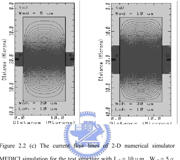
Figure 2.2 The current flow lines of 2-D numerical simulator MEDICI simulation for the differential structure……….. 24
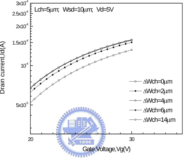
Figure 2.3 ID-VG curve with different W△ ch... 26
Figure 2.4 Average On-state drain current virus W△ ch for different channel length………... 30
Figure 2.5 Side current ration virus W△ ch for different channel length…………. 31
Figure 2.6 Average leakage current virus W△ ch for channel length is 15 μm….. 32
Figure 2.7 The maximum drain current and minimum of-state current virus W △ ch for channel length is 15 μm………. 33
Figure 3.1 The critical five-lithography fabrication procedures……….. 34
Figure 3.2 The critical four-lithography fabrication procedures……….. 36
Figure 3.3 Top view of the proposed staggered structure……… 40
Figure 3.4 ID - VG curve for Lch = 3 μm, W = 5 μm and Vd = 5 V for different S/D width……… 41
Figure 3.5 ID - VG curve for Lch = 3 μm, W = 10 μm and Vd = 5 V for different S/D width……… 42
Figure 3.6 ID - VG curve for Lch = 15μm, W = 5μm and Vd = 5 V for different S/D width……… 43
Figure 3.7 ID - VG curve for Lch = 15 μm, W = 10 μm and Vd = 5 V for different S/D width……… 44
Figure 3.8 ID - VG curve for Lch = 3μm, W = 5μm and Vd = 5 V for the proposed staggered structure, conventional staggered structure and conventional co-planar structure……….. 45
Figure 3.9 ID - VG curve for Lch = 3 μm, W = 10 μm and Vd = 5 V for the proposed staggered structure, conventional staggered structure and conventional co-planar structure………. 46
Figure 3.10 ID - VG curve for Lch = 15 μm, W = 5 μm and Vd = 5 V for the proposed staggered structure, conventional staggered structure and conventional co-planar structure………. 47
Figure 3.11 ID - VG curve for Lch = 15 μm, W = 10 μm and Vd = 5 V for the proposed staggered structure, conventional staggered structure and conventional co-planar structure………. 48
Chapter 1
Introduction
1.1 Overview of Low Temperature Poly-Si TFTs
Polycrystalline silicon thin-film transistors (poly-Si TFTs) have been intensively studied for application to high performance large-area active matrix liquid-crystal display (AMLCD) systems [1]. In the past, amorphous silicon thin-film transistors (a-Si:H TFTs) are mainly used for active-matrix addressed LCDs. However, the low carrier mobility (< 1 cm2V-1S-1) achieved with these devices limits the technology from being developed to form integrated drive circuits on the active matrix plate. Compared with amorphous-Si TFTs, the major advantages of applying poly-Si TFTs on AMLCDs are the larger carrier mobility and the lower photocurrent and better reliability [2]. In poly-Si film, carrier mobility larger than 100 cm2/Vs can be easily achieved, give rise to the capability of serving as peripheral driving circuit [3].
However, some problems still exist in applying poly-Si TFTs on large-area displays. When poly-Si film is serving as device channel layer, the complex grain structure in poly-Si has strong influences on device characteristics. Large amount of defects serving as trap states locate in the disordered grain boundary regions to degrade the on-state current seriously [4] . These traps also enable valence-band carriers jumps to conduction band via trap-assisted thermionic emission or trap-assisted thermionic field emission, leading to large leakage current [5,6]. Therefore, some special structure such as lightly-doped drain region (LDD) is used to effectively lower leakage current by decreasing drain electric field [7,8]. However, LDD structure indeed reduced the electric field but also introduces high source/drain
series resistance which limits the on-state current. Besides, an extra mask in LDD structures is a major problem. There, how to reduce off-state current without degrade on-state current is very important. Recently, a study on the influence of lateral electric field on the leakage current has been reported [9]. It was found that the high lateral electric field at the channel/drain junction can be effectively reduced by use of a thick drain but thin channel structure. In my thesis, I will discuss the electrical properties of a new structure with thick S/D and wider channel region.
1.2 Methods of device parameter extraction
In the section, the methods of extracting typical parameters such as threshold voltage, on-off current ration from device characteristics are briefly introduced.
1.2.1 Determination of threshold voltage (V
th)
Threshold voltage (Vth) is an important parameter required for channel length-width and series resistance measurement. However, Vth is a voltage which is not uniquely defined. Plenty ways are used to determinate the threshold voltage. The method to determinate the threshold voltage in my thesis is the constant drain current method which the voltage at a specific drain current IN is taken as the threshold voltage. Typically, the threshold current IN=ID/(W/L) is specified at 100 nA for VD=5V in most papers to extract the threshold voltage of TFTs.
1.2.2 Determination of On/Off Current Ratio
means not only large On current but also small leakage current. In poly-Si TFTs, The leakage current resulted from carrier generation from the poly-Si grain boundary defects. The carrier generation from grain boundary defects via thermionic emission is the dominant mechanism at a low drain bias, and carrier tunneling from grain boundary defects is the dominant mechanism at higher drain bias [10]. Because of the channel is composed of poly crystalline, a large amount of trap densities in active region. Therefore, the leakage current due to the tunneling effect is very serious.
There are some ways to specify the on-state current and off-state current. In my thesis, take n-channel poly-Si TFTs for examples, the on-state current and off-state current are defined as the drain current when gate voltage is 30V and drain voltage is 5V. The off current is specified as the minimum leakage current in linear operation mode for usual cases.
1.3 Motivations
In order to improve on/off current ration, we try to decrease the off-state current and increase the on-state current. In other studies, the thicker source/drain can help reduce the lateral electric field near the drain junction and then reduce the off-state current. However, using this fabrication needs additional mask to define active region. In my thesis, we propose a new fabrication with four masks completing it. And a test structure with a fixed source/drain width but a wider channel width have been used to discuss the influences of the source/drain width and the channel width on the drain current in both on and off state.
In chapter 1, we introduce a brief overview of LTPS TFT structure and describe some device parameter extraction methods.
In chapter 2, we will show the electrical characteristic of the test structure with wider channel width.
In chapter 3, we will discuss the electrical characteristic of our proposed staggered structure with thicker S/D and wider channel.
Chapter 2
Experimental results and simulations of Low-Temperature
poly-Si TFTs with wider channel
2.1 Introduction
The drain current models of poly-Si TFTs and MOSFETs related to the channel width have been well defined in precious literatures [11]-[16]. In these models, the channel widths are assumed to be identical with S/D width. However, there are no precious articles discussed with the variations of the drain current when the channel width is not identical to the S/D width. In this study, we used a test structure with a channel width that is wider than a fixed S/D width, as shown in Figure 2.1, to investigate the variation of drain current in both on and off state. We also show the simulation results of 2-D numerical simulator MEDICI.
2.2 Device fabrication
The poly-Si TFTs were fabricated on 6-inch-diameter n-type silicon wafer. At first, amorphous silicon (a-Si) films with a thickness of 50nm were deposited on thermally oxidized Si wafers by LPCVD system at 550°C with SiH4 as the gaseous source. Then the solid phase crystallization (SPC) process was carried out with 600°C for 24 hours. After the first lithography step, the poly silicon layer then was defined as the active region. Here we used the TCP poly-etcher system to etch other poly-Si film. A 50nm-thick TEOS oxide film was deposited at 350°C to serve as the gate dielectric by PECVD. Then, a 300nm-thick poly-Si was deposited by LPCVD at 620°C with
SiH4 for the gate electrode. The active region was doped by 5E15 ions/cm2 phosphorus implantation at a 30Kev of acceleration voltage. The dopants were activated at 600°C in N2 ambient for 24 hours. Next, a 300nm oxide was deposited by PECVD at 350°C as a passivation layer, and contact lithography was carried out. After opening contact holes, a 500nm Al was deposited by evaporation and the metal layer was patterned. Finally, the samples were sintered at 400° C for 30 minutes in N2 gas ambient. After completing the device fabrication, no hydrogenation step was performed.
The detailed fabrication process flows are listed as follow: 1. (100) orientation Si wafer
2. Initial cleaning
3. Thermal wet oxidation at 980°C to grow 500nm thermal SiO2 in furnace 4. 50nm a-Si was deposited by LPCVD at 620°C in SiH4 gas
5. SPC crystallization
6. Mask#1: define active regions 7 Poly-Si dry etch by TCP system
8. 50nm TEOS oxide deposition by PECVD at 350°C
9. 300nm poly-Si was deposited by LPCVD at 620°C in SiH4 gas 10. Mask#2: Define gate regions
11. Poly-Si dry etch by TCP system 12. Ion implantation: PP
31, 5×1015 cm-2, 30 KeV 13. Dopant activation in N2 ambient at 600°C for 24 hr
14. 300 nm TEOS oxide film was deposited by PECVD at 350°C for the passivation 15. Mask#3: Open contact holes
16. Wet etching by B.O.E
18. Mask#4: Al pattern defined
19. Etching Al and removing photoresist
20. Al sintering at 400°C in N2 ambient for 30 minutes
2.3 The device parameters
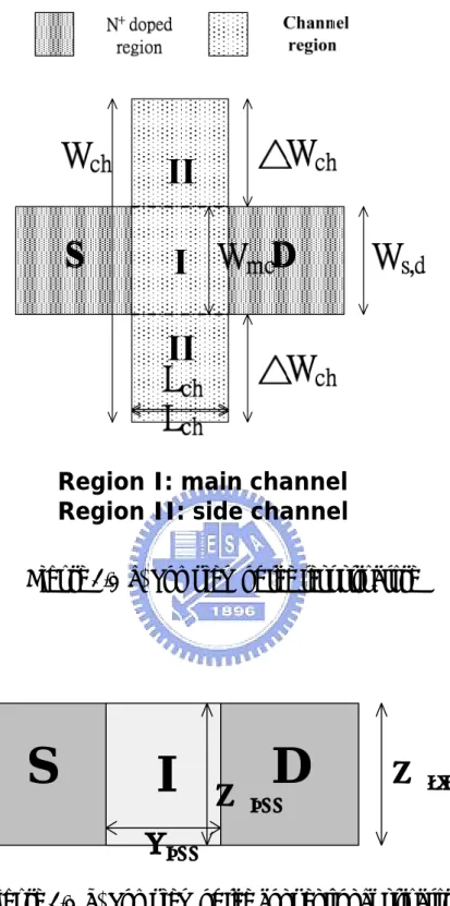
Top view of the test structure is shown in Figure 2.1(a). In this Figure, the channel region are divided into two part (regionⅠand region Ⅱ), and the channel length and width are represented as Lch and Wch. The channel width (Wch) is wider than the S/D width(Wsd) , and the channel width can be written as
Wch = Wm.c + 2ΔWch
where ΔWch is the width of the side channel region (region II in Figure 2.1(a)) in the test structure, and Wm.c is the main channel width and is equal to source/drain width (Wsd). In the test structure, the main channel width (Wm.c) is 5μm and 10μm, respectively. And the side channel widths (ΔWch)are 0μm, 2μm, 4μm, 6μm, 10μm, and 14μm, respectively. When ΔWch is 0μm, it is the conventional poly-Si TFTs structure for comparison as shown in Figure 2.1(b)
2.4 The simulation of 2-D numerical simulator MEDICI
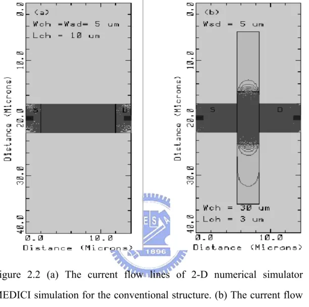
In this part, we use the 2-D numerical simulator MEDICI to simulate the current flows of the test and conventional structures. Figure 2.2(a) shows the simulated current flow lines of the conventional structure at on state. The channel length is 10μm and channel width is 5μm. In Figure 2.2(a), we can find that the current flow lines of the conventional structure are uniformly distributed in the channel region and source/drain region. In Figures 2.2(b), 2.2(c), and 2.2(d), the test structures with
different channel lengths and S/D widths were simulated. From the three Figures, we can see that there are additional current flow paths different from the conventional sample existed in the side channel region. Further, compared with Figure 2.2(b) and 2.2(c), when the channel length is increased from 3μm to 10μm, more current flow lines exist in the side channel region. Compared with Figure 2.2(c) and 2.2(d), it is seen that, even when the S/D width increases from 5μm to 10μm, the distributions of current flow lines in regionⅡ are almost the same. Moreover, we can find that the current flow lines in the side channel regions would almost distribute in the certain width. The certain width is smaller than the all side channel width and it seems only related to the channel length when the side channel width is large. Therefore, we can predict that a saturation value of certain side width exists. From these results of simulations, we can get some inference as follows:
(1) The current flow lines can exist in the side channel region. If we increase the side channel region, the on-current of the test structure should be enlarged.
(2) If the channel length is increased, there will be more current flow lines in the side channel region.
(3) The side current flow lines distribute in the certain side width but not in the all side width. In addition, the certain side width should be related to the channel length.
2.5 The experimental results of the test structure
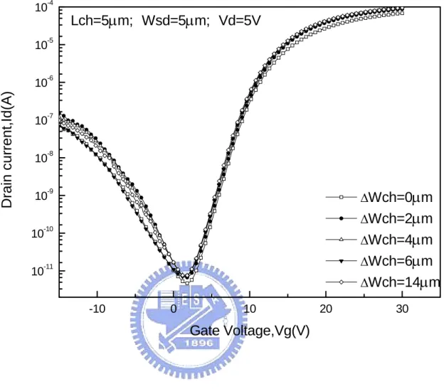
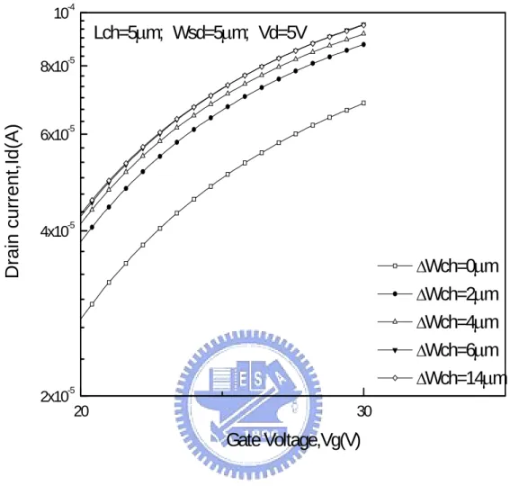
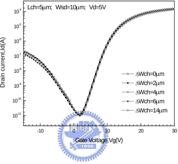
In this part, we will discuss the device performance of our test structure and the comparison with the conventional structure. The ID-VG curve for the test structures which have the channel length of 5 μm, S/D width of 5 μm and 10 μm and drain voltage of 5 V are shown in Figure 2.3. In Figures 2.3 (b) and (d), it is seen that drain current would be increased with the increasing side channel width (ΔWch). In order to
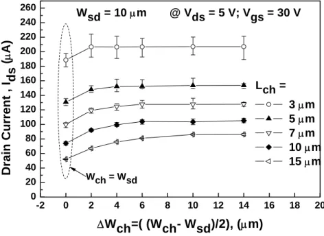
receive more accurate results, we averaged the value of on-state current for the test structures that have the same device parameters. In Figures 2.4 (a) and (b), the channel length is changed from 3 μm to 15 μm and the S/D width is 10 μm and 5 μm, respectively. The drain voltage is 5 V and the gate voltage is 30 V. We can see that they have the same tendency and it can be fitted the first result of simulations. To further investigate the relationship of the drain current and the side channel width, it can be found that the drain current would be saturated when the side channel is large enough. Moreover, as the channel length decreasing (such as Lch = 3 μm), the drain current would be gradually independent of side channel width. It indicates that the currents flow in the side channel region would be decreased when the channel length decrease. These experimental results accord with our preceding second expectancy. Next, we analyze the increasing ratio of the drain current for the test structure. Here we define the drain current gain (Ai) as follows:
, ,
( ) /
i ds t ds c ds,c
A = I −I I
where Ids,t is the drain current of the test structure and Ids,c is the drain current of the conventional structure. Therefore, Ids,t–Ids,c is the drain current flowed via side channel region. In Figures 2.5 (a) and (b), it can be observed that the drain current gain of the test structures have a linear region and a saturation region. In linear region, the drain current gain is dependent on ΔWch. In the saturation region, current gain becomes independent on ΔWch. It implies that there will be a saturation value of side current distribution width existed and also proves the third conclusion of simulations. Therefore, it is convinced that drain current in on state is not only related to the S/D width but also related to the channel width.
In Figure 2.6, we observe the variation of leakage current. It is well known that the leakage current for poly-Si TFT is related to grain boundary traps and electric
field near the drain region [10]. It implies that the drain region width would affect the leakage current. In Figure 2.6, we can see that the leakage current is not related to the side channel width. Therefore, the leakage current will not be added or reduced in our test structure.
Figure 2.7 shows the maximum on state current (Id,max) , the minimum off state current (Id,min) and the on/off current ratio measured at maximum on state current and minimum off state current. In figure 2.7 (b), it is observed that poly-Si TFT with wider channel width would improve the on/off current ration from 8.85 × 10⁶ to 1.14 × 10⁷ . Therefore, the poly-Si TFT structure with fixed S/D width and wider channel width would significantly increase the on state current and obtain a larger on/off current ratio.
2.6 Conclusion
In this chapter, we investigate the influences of the channel width and S/D width on the drain current at both 〝on〞 and 〝off〞 state. At on state, the drain current is enlarged by increasing the side channel width and this is because the additional current flow paths existed in the side channel region. On the contrary, at off state, the drain leakage current is not obviously related to the side channel width. These conclusions are listed as follows:
(1) The current flow lines can exist in the side channel region. If we increase the side channel region width, the on-state current of the test structure should be increased. (2) If the channel length is increased, there will be more current flow lines existed in the side channel region.
(3) The side current flow lines distribute within a certain side channel width. Besides, this width should be related to the channel length.
Chapter 3
Experimental of Low-Temperature poly-Si TFTs with thick
S/D and thin channel
3.1 Introduction
In poly-Si TFTs, the dominant leakage current mechanism has been reported. It arises from the field emission via grain boundary by a high electric field near the drain [10]. Recently, some studies on the influence of lateral electric field on the anomalous leakage current of poly-Si TFTs has been reported [9,17]. It was found that the high lateral electric field at the channel/drain junction can be effectively reduced by use of a thicker source/drain but thinner channel structure. However, this fabrication will need five lithography steps. In this chapter, we will discuss the device performance of our novel staggered structure of poly-Si TFTs (4-masks) and the comparisons of our structure with the conventional staggered structure (5-masks) and conventional co-planar structure (4-masks) are also shown.
3.2 Device fabrication
The conventional staggered poly-Si TFTs were fabricated on 6-inch-diameter n-type silicon wafer. The fabrication process flow is as follows. At first, amorphous silicon (a-Si) films with three kinds of thickness (100nm, 200nm, and 300nm) were deposited on thermally oxidized Si wafers by LPCVD system at 620°C with SiH4 as the gaseous source. After the first lithography step, we used the TCP system to etch amorphous silicon films. Then amorphous silicon (a-Si) films with a thickness of
50nm were deposited on thermally oxidized Si wafers by LPCVD system at 620°C with SiH4 again. Then the solid phase crystallization (SPC) process was carried out with 600°C for 24 hours. After the second lithography step, the poly silicon layer was then defined as the active region and we used the TCP poly-etcher system to etch other poly-Si film. A 50 nm-thick TEOS oxide film was deposited at 350°C to serve as the gate dielectric by PECVD. Then, a 300 nm-thick poly-Si was deposited by LPCVD at 620°C with SiH4 for the gate electrode and the third lithography step was used to define gate region. The active region was doped by 5E15 ions/cm2 phosphorus implantation at a 50 KeV(100nm), 70 KeV(200nm), and 100 KeV(300nm) of acceleration voltage. The dopants were activated at 600°C in N2 ambient for 24 hours. Next, a 300-nm oxide was deposited by PECVD at 350°C as a passivation layer, and contact lithography was carried out. After opening contact holes, a 500-nm Al was deposited by evaporation and the metal layer was patterned. Finally, the samples were sintered at 400° C for 30 minutes in N2 gas ambient. After completing the device fabrication, no hydrogenation step was performed. Therefore, this fabrication needs five lithography steps.
However, in our proposed staggered structure, after the second amorphous silicon (a-Si) films with a thickness of 50-nm were deposited, the SPC was carried out. The second a-Si films were removed after defining gate region. Therefore, the channel width should be wider than the S/D width in our proposed staggered structure as shown in Figure 3.3 and this new fabrication only need four lithography steps.
The critical five-lithography fabrication procedures are shown in Figure 3.1 and listed as follows:
1. Thermal wet oxidation at 980°C to grow 500 nm thermal SiO2 in furnace
2. α-Si (100 nm, 200 nm and 300 nm) film was deposited by LPCVD at 620°C in SiH4 gas
3. Mask#1: define S/D island
4. α-Si (50nm) film was deposited by LPCVD at 620°C in SiH4 gas 5. SPC was carried out with 600°C for 24 hrs
6. Mask#2: define active region
7. 50 nm TEOS gate dielectric deposition by PECVD at 350°C
8. 300 nm poly-Si gate was deposited by LPCVD at 620°C in SiH4 gas 9. Mask#3: define gate region
10. Poly-Si film was dry etched by TCP system
11. Ion implantation: P31, 5×1015 cm-2, 50 KeV (100 nm), 70 KeV (200 nm) ,100 KeV (300 nm)
12. Dopant activation in N2 ambient at 600°C for 24 hr
13. 300 nm TEOS oxide film was deposited by PECVD at 350°C for the passivation layer
14. Mask#4: open contact holes 15. Wet etching by B.O.E
16. 500 nm Al thermal evaporation 17. Mask#5: Al pads definition
18. Etching Al and removing photoresist
19. Al sintering at 400°C in N2 ambient for 30 min
The critical four-lithography fabrication procedures are shown in Figure 3.2 and listed as follows:.
1. Thermal wet oxidation at 980°C to grow 500 nm thermal SiO2 in furnace 2. α-Si (100 nm, 200 nm and 300 nm) film was deposited by LPCVD at 620°C in
SiH4 gas
3. Mask#1: define S/D island
5. SPC was carried out with 600°C for 24 hrs
6. 50 nm TEOS gate dielectric deposition by PECVD at 350°C
7. 300 nm poly-Si gate was deposited by LPCVD at 620°C in SiH4 gas 8. Mask#2: define gate region
9. Poly-Si film was dry etched by TCP system 10. Ion implantation:
11. Dopant activation in N2 ambient at 600°C for 24 hr
12. 300 nm TEOS oxide film was deposited by PECVD at 350°C for the passivation layer
13. Mask#3: open contact holes 14. Wet etching by B.O.E
15. 500 nm Al thermal evaporation 16. Mask#4: Al pads definition
17. Etching Al and removing photoresist
18. Al sintering at 400°C in N2 ambient for 30 min
3.3 The experimental results of the proposed staggered structure
Figures 3.4~3.7 show the ID-VG curve of our proposed structure with different S/D thickness. We can see that the leakage current (at Vgs = -15 V) is reduced by increasing the thickness of source/drain. It is due to that the proposed structure has a thicker S/D to reduce the lateral electric field near the drain junction. Next, we compare the conventional co-planar structure, conventional staggered structure and our proposed staggered structures. In our proposed structure, the channel width is wider than the S/D width. However, the channel width is identical to the S/D width in conventional staggered structure. In Figures 3.8~3.11, we use the different channel
length (Lch = 3 μm and Lch = 15 μm) and different S/D width (Wsd = 5 μm and Wsd = 10 μm) to compare the transfer characteristics. Although these device parameters are different, these transfer characteristics have the same tendency. As shown in table 1~4, for the two kinds of staggered structures, the leakage currents (at Vgs = -15 V) are all smaller than convention co-planar structure. In addition, the drain currents of the conventional staggered structure are almost the same as the conventional co-planar structure at on-state. These results are responsible with previous literatures [9,17].
Owing to the existence of the side current flows, the drain currents of our proposed staggered structure with wider channel width would be larger than the conventional stagger structure in on-state(VG = 30 V) . Moreover, the drain currents of our proposed staggered are obviously larger than the conventional co-planar structure when the channel length is 15μm. This result fits the second conclusion in chapter 2. Further, it can be seen that the minimum drain currents are also enlarged. It also results from the side current flows.
In table 1 ~ 4, it can be seen that on/off ratio of our proposed staggered structure is decreased. In off state, compared with conventional staggered structure and conventional co-planar structure, the leakage current of the conventional staggered structure is larger than that of the co-planar structure. It is due to more grain boundary traps exist in the thick channel regions near the S/D region. Moreover, compared with the conventional staggered structure and the proposed structure, the leakage current of the proposed structure is larger than that of the conventional staggered structure. However, it is due to that the side channel current would increase the drain leakage current. Therefore, the on/off current ratio of our proposed structure is smaller than the conventional co-planar structure. Although, the on/off current ratio is smaller, the drain leakage current (at Vgs = -15 V) would significantly decrease about one order. Therefore, our proposed staggered structure can not only enlarge on-state current but
also decrease the leakage current (at Vgs = -15 V). Of course, it also can reduce our cost because it needs only four masks.
3.4 Conclusion
In this chapter, we discuss the electrical properties of the novel structures with thicker S/D width and wider channel length. The drain leakage current (at Vgs = -15 V) would be decreased and the on-state current would be increased. However, the on/off ratio is also decreased.
Chapter 4
Conclusion and future work
4.1 Conclusion
In this thesis, we first discuss the influences of the channel width and S/D width on the drain current at both on-state and off-state. Then we use these results to discuss the electrical properties of the novel staggered structure with thicker S/D region and wider channel region. The drain current at on-state will be enlarged and the leakage current (Vgs = -15V) will be decreased. In our fabrication process, we only need four lithography steps. Therefore, the novel structure of thicker S/D region and wider channel region exhibits superior electrical characteristics to the conventional co-planar structure. Hence, the proposed high performance poly-Si TFTs are promising for the application of integrated circuits on LCS panel.
4.2 Future work
We have proposed a novel low-temperature poly-Si TFTs with a thicker source/drain region and wider channel to improve the conventional low-temperature poly-Si TFTs performance. In order to further improve electrical properties of our devices, there will be still some works worth of being investigated.
In our experiment, the minimum leakage current of the proposed structures was increased due to large number of the grain boundary traps near the drain region existence. It is well known that NH3 or H2 plasma could significantly reduce the grain boundary traps due to the formation of S≣N and S-H bonds [18]. In addition, we also can establish the drain current model of the test structure with wider channel region.
Reference
[1] T.Serilawa, S.shirai, A. Okamoto, and S. Suyama, “Low-temperature fabrication
of high-mobility Poly-Si TFTs for large-area LCD’s,” IEEE Trans. Electron Dev.,
vol. 36, no. 9, pp. 1929,1989.
[2] J. R. Ayres and N. D. Young, “Hot carrier effects in devices and circuits formed
from poly-Si,” IEEE proc. Circuits Devices Syst., vol. 131, no. 1, p.38, 1994.
[3]S.D Brotherton, “Topical review:Polycrystalline silicon thin film transistors,”
Sci.Technoi., vol.10, pp721-738, 1995.
[4] J. Levinson, F. R. Shepherd, P. J. Scanlon, W. D. Westwood, G. Este, and M. Rider,
“Conductivity behavior in polycrystalline semiconductor thin film transistors,” J.
Appl. Phys. Vol. 53, pp.1193-1202, 1982
[5] P. Migliorato, C. Reita, G. Tallatida, M. Quinn and G. Fortunato, “Anomalous
off-current mechanisms in n-channel poly-Si thin film transistors.”
Solid-State-Electronics, Vol.38, pp.2075-2079, 1995
[6] M. Hack, I-W. Wu, T. H. King and A. G. Lewis, “Analysis of Leakage Currents in
Poly-silicon Thin Film Transistors,” IEDM Tech. Dig., vol. 93, pp. 385-387, 1993
[7] Byung-Hyuk Min and Jerzy Kanicki, “Electrical characteristics of new LDD
poly-Si TFT structure tolerant to process misalignment,” IEEE Electron Device
Lett., vol. 20, pp. 335-337, 1999
[8] Shengdong Zhang, Ruqi Han, and Mansun J. Chan, “A novel self-aligned bottom
gate poly-Si TFT with in-situ LDD,” IEEE Electron Devices Lett., vol. 22, pp.
393-395, 2001.
[9] A. Kumar K.P. and J. K. O Sin, “Influence of lateral electric field on the
anomalous leakage current in polysilicon TFT,” IEEE Electron Device Lett, vol.
[10]K.R.Olasupo and M.K.Hatalis, “Leakage current mechanism in sub-micron
polysilicon Thin-Film Transistors,” IEEE Trans. Electron Device, vol. 43, no.8,
pp.1218-1223, 1996
[11] S. M. Sze, Physics of Semiconductor Devices, 2nd ed., Taiwan: John Wiley &
Sons, 1981, pp. 433-448.
[12] Gi-Young Yang, Sung-Hoi Hur, and Chul-Hi Han, “A Physical-Based Analytical
Turn-On Model of Polysilicon Thin-Film Transistors for Circuit Simulation,”
IEEE Trans. Electron Devices, vol.46, no.1, pp.165-172, Jan. 1999.
[13] Hsin-Li Chen and Ching-Yuan Wu, “A New I-V Model Considering the
Impact-Ionization Effect Initiated by the DIGBL Current for the Intrinsic
n-Channel Poly-Si TFT’s,” IEEE Electron Device Letters, vol. 46, no. 4, pp.
772-728, Apr. 1999.
[14] Peyman Servati, and Arokia Nathan, “Modeling of the Reverse Characteristics of
a-Si:H TFTs,” IEEE Trans. Electron Devices, vol.49, no.5, pp.812-819, May.
2002.
[15] Horng Nan Chern, Chung Len Lee, and Tan Fu Lei, “An Analytical Model for
the Above-Threshold Characteristics of Polysilicon Thin-Film Transistors,” IEEE
Trans. Electron Devices, vol.42, no.7, pp.1240-1246, Jul. 1995.
[16] Filippos V. Farmakis, Jean Brini, George Kamarions, Constantinos T. Angelis,
Charalambos A. Dimitriadis, and M. Miyasaka, “On-Current Modeling of
Large-Grain Polycrystalline Silicon Thin-Film Transistors,” IEEE Trans.
Electron Devices, vol.48, no.4, pp.701-706, Apr. 2001.
[17] Ching-Wei Lin; Li-Jing Cheng; Yin-Lung Lu; Yih-Shing Lee; Huang-Chung
Cheng , “High-performance low-temperature poly-Si TFTs crystallized by
excimer laser irradiation with recessed-channel structure,” IEEE Electron Device
[18] W. Wu, W. B. Jackson, T. Y. Huang, A. G. Lewis, and A. C. Chiang,
“Passivation kinetics of two types of defects in polysilicon TFT by plasma
hydrogenation,” IEEE Electron Device Lett., vol. 12, no. 5, pp. 181–183, May
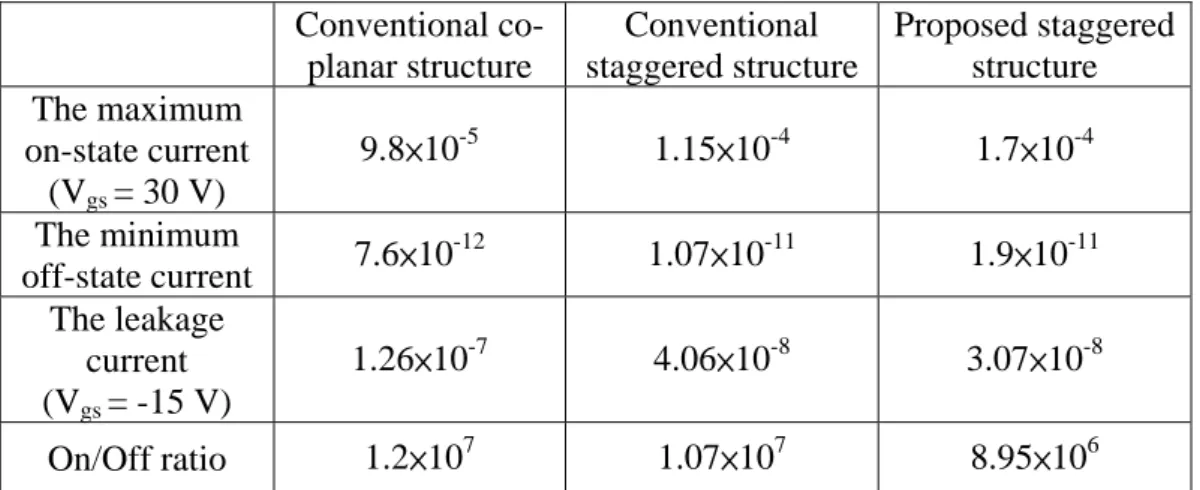
Table 1 Conventional co-planar structure Conventional staggered structure Proposed staggered structure The maximum on-state current (Vgs = 30 V) 9.8×10⁻⁵ 1.15×10⁻⁴ 1.7×10⁻⁴ The minimum off-state current 7.6×10 -12 1.07×10⁻¹¹ 1.9×10⁻¹¹ The leakage current (Vgs = -15 V) 1.26×10⁻⁷ 4.06×10⁻⁸ 3.07×10⁻⁸ On/Off ratio 1.2×10⁷ 1.07×10⁷ 8.95×10⁶
Table 1: Compared with the maximum on-state current (Vgs = 30 V), the minimum off-state current and the leakage current (Vgs = -15 V ). The channel length (Lch) is 3 μm, S/D width (W) is 5μm, and drain voltage ( Vds ) is 5 V.
Table 2 Conventional co-planar structure Conventional staggered structure Proposed staggered structure The maximum on-state current 1.97×10 -4 2.06×10⁻⁴ 2.65×10⁻⁴ The minimum off-state current 1.33×10 -11 1.69×10⁻¹¹ 2.44×10⁻¹¹ The leakage current (Vgs = -15 V) 3.7×10⁻⁷ 5.2×10⁻⁸ 6.2×10⁻⁸ On/Off ratio 1.48×10⁷ 1.19×10⁷ 1.1×10⁷
Table 2: Compared with the maximum on-state current (Vgs = 30 V), the minimum off-state current and the leakage current (Vgs = -15 V ). The channel length (Lch) is 3 μm, S/D width (W) is 10μm, and drain voltage ( Vds ) is 5 V.
Table 3 Conventional co-planar structure Conventional staggered structure Proposed staggered structure The maximum on-state current 2.7×10 -5 2.56×10⁻⁵ 6.3×10⁻⁵ The minimum off-state current 2.6×10 -12 5.1×10⁻¹² 8.57×10⁻¹² The leakage current (Vgs = -15 V) 1.9×10⁻⁷ 2.8×10⁻⁸ 1.8×10⁻⁸ On/Off ratio 1.04×10⁷ 5.02×10⁶ 7.35×10⁶
Table 3: Compared with the maximum on-state current (Vgs = 30 V), the minimum off-state current and the leakage current (Vgs = -15 V ). The channel length (Lch) is 15 μm, S/D width (W) is 5μm, and drain voltage ( Vds ) is 5 V.
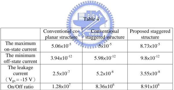
Table 4 Conventional co-planar structure Conventional staggered structure Proposed staggered structure The maximum on-state current 5.06×10 -5 5×10⁻⁵ 8.73×10⁻⁵ The minimum off-state current 3.94×10 -12 5.98×10⁻¹² 9.8×10⁻¹² The leakage current (Vgs = -15 V) 2.5×10⁻⁷ 5.2×10⁻⁸ 3.55×10⁻⁸ On/Off ratio 1.28×10⁷ 8.36×10⁶ 8.91×10⁶
Table 4: Compared with the maximum on-state current (Vgs = 30 V), the minimum off-state current and the leakage current (Vgs = -15 V ). The channel length (Lch) is 15 μm, S/D width (W) is 10μm, and drain voltage ( Vds ) is 5 V.
Region I: main channel
Region II: side channel
Figure 2.1(a) Top view of the test structure
S
D
W
s,d
L
ch
W
ch
I
Figure 2.2 (a) The current flow lines of 2-D numerical simulator
structure with L
ch= 3μm , W
sd= 5μm.
MEDICI simulation for the conventional structure. (b) The current flow
lines of 2-D numerical simulator MEDICI simulation for the test
Figure 2.2 (c) The current flow lines of 2-D numerical simulator
MEDICI simulation for the test structure with L
ch= 10μm , W
sd= 5μ
m.(d) The current flow lines of 2-D numerical simulator MEDICI
simulation for the test structure with L
ch= 10μm , W
sd= 10μm.
-10 0 10 20 30 10-11 10-10 10-9 10-8 10-7 10-6 10-5 10-4
Lch=5
μ
m; Wsd=5
μ
m; Vd=5V
ΔWch=0
μ
m
ΔWch=2
μ
m
ΔWch=4
μ
m
ΔWch=6
μ
m
ΔWch=14
μ
m
D
ra
in
c
u
rre
n
t,Id
(A
)
Gate Voltage,Vg(V)
20 30 2x10⁻⁵ 4x10⁻⁵ 6x10⁻⁵ 8x10⁻⁵ 10-4
Lch=5
μ
m; Wsd=5
μ
m; Vd=5V
ΔWch=0
μ
m
ΔWch=2
μ
m
ΔWch=4
μ
m
ΔWch=6
μ
m
ΔWch=14
μ
m
Drain current,I
d(A)
Gate Voltage,Vg(V)
-10 0 10 20 30 10-11 10-10 10-9 10-8 10-7 10-6 10-5 10-4 ΔWch=0
μ
m ΔWch=2μ
m ΔWch=4μ
m ΔWch=6μ
m ΔWch=14μ
m Drain curr ent ,I d(A ) Gate Voltage,Vg(V) Lch=5μ
m; Wsd=10μ
m; Vd=5V20 30 5x10⁻⁵ 10-4 1.5x10⁻⁴ 2x10⁻⁴ 2.5x10⁻⁴ 3x10⁻⁴ Δ
Wch=0
μ
m
ΔWch=2
μ
m
ΔWch=4
μ
m
ΔWch=6
μ
m
ΔWch=14
μ
m
Drain cur
rent
,I
d(A)
Gate Voltage,Vg(V)
Lch=5
μ
m; Wsd=10
μ
m; Vd=5V
-2 0 2 4 6 8 10 12 14 16 18 20 0 20 40 60 80 100 120 140 160 180 200 220 240 260 Wch = Wsd Lch = 3 μm 5 μm 7 μm 10 μm 15 μm Dra in Cu rren t , I ds ( μ A) ΔWch=( (Wch- Wsd)/2), (μm) Wsd = 10 μm @ Vds = 5 V; Vgs = 30 V
Figure 2.4(a) Average On-state drain current virus △W
chat W
sd= 10
μmm, V
ds= 5 V and V
gs= 30 V for different channel length
-2 0 2 4 6 8 10 12 14 16 18 20 0 10 20 30 40 50 60 70 80 90 100 110 120 130 140 150 Wsd = 5 μm @ Vds = 5 V; Vgs = 30 V Lch = 3 μm 5 μm 7 μm 10 μm 15 μm ΔWch=( (Wch- Wsd)/2), (μm) Dr ain Cur re nt , I ds ( μ A)
Figure 2.4(b) Average On-state drain current virus △W
chat W
sd= 5
μm,
-2 0 2 4 6 8 10 12 14 16 18 20 0 10 20 30 40 50 60 70 80 saturation region W sd = 10 μm @ Vds = 5 V; Vgs = 30 V A i = (I ds, t - I ds, c )/I ds, c , (%) ΔW ch=( (Wch- Wsd)/2), (μm ) Lch = 3 μm 5 μm 7 μm 10 μm 15 μm linear region
Figure 2.5(a) side current ration virus △W
chat W
sd= 10
μm,V
ds= 5 V
and V
gs= 30 V for different channel length
-2 0 2 4 6 8 10 12 14 16 18 20 0 20 40 60 80 100 120 Wsd = 5 μm @ Vds = 5 V; Vgs = 30 V Lch = 3 μm 5 μm 7 μm 10 μm 15 μm A i = (I ds, t - I ds, c )/I ds ,c , (%) ΔWch=( (Wch- Wsd)/2), (μm)
Figure 2.5(b) side current ration virus △W
chat W
sd= 5
μm,V
ds= 5 V
-2 0 2 4 6 8 10 12 14 16 -200 0 200 400 600 800 1000 1200 1400 1600 1800 2000 Drain l eak age Curre nt , (nA) ΔW ch=( (W ch- Wsd)/2), (μm) Vds = 5 V Vds = 10 V W sd = 10 μm Lch = 15 μm @ Vgs = -15 V
Figure 2.6(a) Average leakage current virus △W
chat W
sd= 10
μm, V
ds=
5 V and 10V, V
gs= -15V for channel length is 15
μm-2 0 2 4 6 8 10 12 14 16 18 20 0 50 100 150 200 250 300 350 400 450 ΔW ch=( (W ch- Wsd)/2), (μm) D rai n l e akage Cu rrent , ( n A ) Vds = 5V Vds = 10V W sd = 5μm ; Lch = 15μm ; Vgs = -15V
Figure 2.6(a) Average leakage current virus △W
chat W
sd= 10
μm,V
ds=
-2 0 2 4 6 8 10 12 14 16 2 3 4 5 6 7 8 9 10 ΔWch=( (Wch- Wsd)/2), (μm)
min. off state current max. on state current
Leakage current ( p A) 20 30 40 50 60 70 80 90 100 Drai n current ( μ A) Conv. Wsd = Wch = 5 μm Wsd/Lch = 5/15 μm/μm @ Vds = 5 V
Figure 2.7(a) the maximum drain current and minimum of-state current
virus △W
chat W
sd= 5
μm, V
ds= 5 V for channel length is 15
μm-2 0 2 4 6 8 10 12 14 16 0.8 0.9 1.0 1.1 1.2 1.3 W sd/Lch = 5/15 μm /μm O n /O ff c u rrent rat io (x1 0 7 ) ΔW ch=( (W ch- W sd)/2), (μm ) Vds = 5 V C o n v. W sd = W ch = 5 μm
Figure 2.7(b) the on/off current ration virus △W
chat W
sd= 5
μm, V
ds=
Figure 3.3(a) Top view of the proposed staggered structure
G
-10 0 10 20 30 10-11 10-10 10-9 10-8 10-7 10-6 10-5 10-4
Drain current
(A
)
Gate voltage(V)
L=3 um; W=5 um; Vd= 5 V
proposed staggered 1000
proposed staggered 2000
proposed staggered 3000
Figure 3.4 I
D- V
Gcurve for L
ch= 3
μm, W = 5
μmand V
d= 5 V for
-10 0 10 20 30 10-11 10-10 10-9 10-8 10-7 10-6 10-5 10-4
Gate voltage(V)
Dr
ain cur
rent
(A)
L=3 um; W=10 um; Vd= 5 V
proposed staggered 1000
proposed staggered 2000
proposed staggered 3000
Figure 3.5 I
D- V
Gcurve for L
ch= 3
μm, W = 10
μmand V
d= 5 V for
-10 0 10 20 30 10-12 10-11 10-10 10-9 10-8 10-7 10-6 10-5 10-4
L=15 um; W=5 um; Vd= 5 V
Drain current
(A)
Gate voltage(V)
proposed staggered 1000
proposed staggered 2000
proposed staggered 3000
Figure 3.6 I
D- V
Gcurve for L
ch= 15
μm, W = 5
μmand V
d= 5 V for
-10 0 10 20 30 10-11 10-10 10-9 10-8 10-7 10-6 10-5 10-4
Dr
ai
n c
u
rr
ent
(A
)
Gate voltage(V)
L=15 um; W=10 um; Vd= 5 V
proposed staggered 1000
proposed staggered 2000
proposed staggered 3000
Figure 3.7 I
D- V
Gcurve for L
ch= 15
μm, W = 10
μmand V
d= 5 V for
-10 0 10 20 30 10-11 10-10 10-9 10-8 10-7 10-6 10-5 10-4 10-3
5-masks conv. staggered
4-masks prop. staggered
conv. co-planar
Drain current
(A)
Gate voltage(V)
L=3 um; W=5 um; Vd= 5 V
Figure 3.8 I
D- V
Gcurve for L
ch= 3
μm, W = 5
μmand V
d= 5 V for the
proposed staggered structure, conventional staggered structure and
conventional co-planar structure.
-10 0 10 20 30 10-11 10-10 10-9 10-8 10-7 10-6 10-5 10-4 10-3
Drain current(A)
Gate voltage(V)
5-masks conv. staggered
4-masks prop. staggered
conv. co-planar
L=3 um; W=10 um; Vd= 5 V
Figure 3.9 I
D- V
Gcurve for L
ch= 3
μm, W = 10
μmand V
d= 5 V for the
proposed staggered structure, conventional staggered structure and
conventional co-planar structure
-10 0 10 20 30 10-12 10-11 10-10 10-9 10-8 10-7 10-6 10-5
5-masks conv. staggered
4-masks prop. staggered
conv. co-planar
D
rain c
u
rr
ent
(A
)
Gate voltage(V)
L=15 um; W=5 um; Vd= 5 V
Figure 3.10 I
D- V
Gcurve for L
ch= 15
μm, W = 5
μmand V
d= 5 V for the
proposed staggered structure, conventional staggered structure and
conventional co-planar structure
-10 0 10 20 30 10-12 10-11 10-10 10-9 10-8 10-7 10-6 10-5 10-4
Drai
n current
(A)
Gate voltage(V)
L=15 um; W=10 um; Vd= 5 V
5-masks conv. staggered
4-masks prop. staggered
conv. co-planar
Figure 3.11 I
D- V
Gcurve for L
ch= 15
μm, W = 10
μmand V
d= 5 V for
the proposed staggered structure, conventional staggered structure and
conventional co-planar structure
簡歷 姓 名:陳正國 性 別:男 出生日期:民國 70 年 3 月 5 日 出 生 地:台灣省新竹市 住 址:彰化縣員林鎮東和里員水路二段 566 巷 26 弄 8 號 學 歷:台中市國立台中一中(民國 85 年 9 月~88 年 6 月) 國立成功大學物理學系(民國 88 年 9 月~92 年 6 月) 國立交通大學電子工程所碩士班(民國 92 年 9 月~95 年 8 月) 碩士論文:具有較厚源/汲極與較寬通道的多晶矽薄膜電晶體的模擬與電性分析
The Simulations and Analysis of The Poly-Si Thin Film Transistor with Thicker S/D and wider Channel