鉍銻碲硒系列拓樸絕緣體長成與物理特性之研究 - 政大學術集成
57
0
0
全文
(2) Abstract. 3D Topological insulator (TI), a type of material that insulates inside bulk and conducts on the surfaces, becomes a popular topic in recent years. The unique topologically protected surface states turn topological insulator to be a potential spintronic material. Bi2Te3 based materials have been studied and identified as topological insulators. In order to study the properties of the surface states, a series of. 政 治 大 tuning the band gap around 立Dirac cone. The lattice structure of Bi. specimens of Bi1.5Sb0.5Te3-ySey (BSTS) with y=1.1, 1.2, 1.4, and 1.6 were fabricated for 1.5Sb0.5Te3-ySey. is. 𝑐̂ are 4.25Å and 29.80Å respectively. substitution. increase.. To. The lattice constants decrease with Se. characterize. the. TI. ‧. ‧ 國. 學. confirmed to be rhombohedral. For the specimen y=1.4 the lattice constants 𝑎̂ and. properties,. the. resistivity,. sit. y. Nat. magnetoresistance and Hall effect were studied. Resistivity showed an insulator. n. al. er. io. behavior at high temperatures and surface conduction behavior at low temperatures.. i n U. v. The dominate carriers are p-type at low temperatures and become n-type at high. Ch. engchi. temperatures. According to the correlations of resistivity and Hall effect of Bi1.5Sb0.5Te3-ySey, we observed that thermal activation can be tuned by Selenium dopants. The weak anti-localization was also observed in our bulk samples. From the 2 K magnetoresistance, we observed that weak anti-localization was independent on Selenium and Tellurium concentrations in all specimens.. I.
(3) 摘要 三維拓樸絕緣體,其擁有表面可以導電但內部卻屬於絕緣體的特殊性質;近 年來成為熱門的研究領域。拓樸保護表面態此種獨特性質使得拓樸絕緣體有潛力 成為自旋電子學研究材料。在已發表的文獻中可以得知 Bi2Te3 系列材料已經被證 實為拓樸絕緣體。我們製作了一系列的 Bi1.5Sb0.5Te3-ySey 材料,希望藉由硒元素 的摻雜改變在狄拉克錐體附近的能帶結構以更詳加了解拓樸絕緣體表面性質以 及其物理特性。他們的晶格結構為菱形六角面體;當摻雜量 y=1.6 時,a 軸及 c. 政 治 大 摻雜量提高而逐漸遞減。為了更進一步了解拓樸絕緣體物理性質,我們做了電阻 立. 軸的晶格常數分別為 4.25 Å 以及 29.80 Å;同時也發現晶格常數隨著硒元素的. ‧ 國. 學. 率、磁阻以及霍爾效應的量測以及分析。電阻率的結果顯示,樣品在高溫時呈現 絕緣體的電阻性質,但在低溫時表面態傳導電子開始主導而電阻上升趨勢轉趨於. ‧. 平緩。在霍爾效應中看到低溫至高溫由 p-type 轉 n-type,並且其變化溫度和硒元. sit. y. Nat. 素摻雜有直接關聯。高溫的 n-type 載子歸咎於於能隙間的 Donor Level 受熱後激. al. er. io. 發電子至傳導帶,最後取代原有的電洞使材料變成 n-type。透過阿瑞尼士方程式,. v. n. 可由電阻對溫度曲線計算其活化能,同時可以了解低溫下電阻反曲及載子型態改. Ch. engchi. i n U. 變之間的關係。我們在磁阻量測中觀察到了弱反局域效應,並且從 2 K 的數據中 顯示此現象和硒元素的摻雜沒有直接關聯性。. II.
(4) Contents Abstract .......................................................................................................................... I 摘要............................................................................................................................... II Contents ....................................................................................................................... III Figure of contents ........................................................................................................IV Table of contents ........................................................................................................... V Chapter 1 Introduction ................................................................................................ 1 1.1 Topological Insulator .................................................................................... 1 1.1.1 2D Topological insulator & Quantum hall state ................................ 3 1.1.2 3D Topological Insulator ................................................................... 7 1.2 Weak Anti Localization................................................................................. 8 1.3 Seebeck Effect .............................................................................................. 9 Chapter 2 Experimental Techniques ......................................................................... 10. 立. 政 治 大. ‧. ‧ 國. 學. 2.1 Equipment & Nomenclature ....................................................................... 10 2.2 Bulk Fabrication.......................................................................................... 11 2.3 X-ray Diffraction ........................................................................................ 14. n. al. er. io. sit. y. Nat. 2.4 Physical property measurement system ...................................................... 15 2.4.1 Resistivity ........................................................................................ 16 2.4.2 Magneto-resistance .......................................................................... 18 2.4.3 Hall Effect ........................................................................................ 19 2.6 Composition Analysis ................................................................................. 22 2.6.1 X-ray Florence ................................................................................. 22 2.6.2 Energy Dispersive Spectrometer...................................................... 22 2.7 Seebeck coefficient measurement ............................................................... 24 Chapter 3 Experimental Results................................................................................ 25 3.1 Composition Analysis ................................................................................. 25 3.1.1 XRF & EDS ..................................................................................... 25 3.1.2 X-Ray Diffraction ............................................................................ 27 3.1.3 Refinement ....................................................................................... 31 3.2 Resistivity ................................................................................................... 35 3.3 Hall measurement ....................................................................................... 39 3.4 Magneto-resistance ..................................................................................... 46. Ch. engchi. i n U. v. Chapter 4 Conclusion and Discussion ...................................................................... 49 Reference ..................................................................................................................... 51. III.
(5) Figure of contents Figure 1.0 3D TI Band structure and Dirac cone ........................................................... 1 Figure 1.1 Landau level for 2D TI ................................................................................. 3 Figure 1.2 Electron’s skipping motion on the edge ....................................................... 5 Figure 1.3 QSH state’s Hall conductivity ...................................................................... 6 Figure 1.4 3D TI Band structure and Dirac cone ........................................................... 6 Figure 1.5 Seebeck effect ............................................................................................... 9 Figure 2.1 (a) Vapor pressure in Pascal ....................................................................... 11 Figure 2.1 (b) Phase Diagram ...................................................................................... 12 Figure 2.2 Anneal pattern ............................................................................................. 13 Figure 2.3 Physical Property Measurement System .................................................... 15 Figure 2.4 Four-probe measurement ............................................................................ 16 Figure 2.7 Hall effect ................................................................................................... 19. 立. 政 治 大. ‧. ‧ 國. 學. Figure 2.8 PPMS puck ................................................................................................. 21 Figure 2.9 XRF-ZSX Primus II ................................................................................... 23 Figure 2.10 EDS on SEM ............................................................................................ 23. n. al. er. io. sit. y. Nat. Figure 2.11 Seebeck measurement system .................................................................. 24 Figure 3.1 MF19 Powder XRD pattern........................................................................ 27 Figure 3.2 Powder XRD Bi2SeTe2 reference (Ref. Pattern00-029-0247) .................... 28 Figure 3.3 Powder XRD pattern .................................................................................. 28 Figure 3.4 Overlap and in large Powder XRD results ................................................. 29 Figure 3.5 Refinement results ...................................................................................... 32 Figure 3.6 Lattice constant ........................................................................................... 33 Figure 3.7 Crystal surface XRD pattern ...................................................................... 34 Figure 3.8 Resistivity measurement ............................................................................. 35 Figure 3.9 Ruler ........................................................................................................... 35 Figure 3.10 Temperature dependence of resistivity ..................................................... 36 Figure 3.11 Second derivative of resistivity ................................................................ 36 Figure 3.12 Se concentration dependence of Resistivity inflection point ................... 37 Figure 3.13 Hall effect measurement ........................................................................... 39 Figure 3.14 Temperature dependence of Carrier concentration ................................... 39 Figure 3.16 Temperature dependence of Hall resistance ............................................. 41. Ch. engchi. i n U. v. Figure 3.17 Band structure of Topological insulator and donor level ......................... 42 Figure 3.19 Resistivity inflection point and Carrier singular point ............................. 44 Figure 3.20 (a) Thermal activation (b)Arrhenius function fitting ................................ 45 Figure 3.21 Resistance at 9T and zero field ................................................................. 46 IV.
(6) Figure 3.22 Magneto-resistance ................................................................................... 47 Figure 3.23 Magneto-resistance at 2K ......................................................................... 48. Table of contents Table 1 Equipment ....................................................................................................... 10 Table 2 Nomenclature .................................................................................................. 10 Table 3 Element composition with XRF ...................................................................... 25 Table 4 Element composition with EDS ...................................................................... 26. 立. 政 治 大. ‧. ‧ 國. 學. n. er. io. sit. y. Nat. al. Ch. engchi. V. i n U. v.
(7) Chapter 1. 1.1. Introduction. Topological Insulator. Topological Insulator has become a hot topic recent. In 2007, the existence of 3D topological insulator were published. After one year later, 3D topological insulator was. 政 治 大 the-art field in solid state physics. 立. successfully found by experiment in Bi-Te bases system. This discovery is the-state-of-. ‧. ‧ 國. 學. n. er. io. sit. y. Nat. al. Ch. engchi. i n U. v. Figure 1.0 3D TI Band structure and Dirac cone (Green line for spin down and orange line for spin down). 3D topological insulators are special materials which insulating inside the bulk but carring the current on its surface. The bulk’s band structure is familiar to a typical insulator which has a gap between valence and conduction band. The carriers would go from valence band to conduction band. This kind of material has particular band structure which exist the special state connecting valence band and conduction band of 1.
(8) electron as Figure 1.0. This unusual states are named the surface state which allowing electron ballistic transport and called Dirac cone. This states are the direct characteristics of topological insulators and the topological phase is determined by nontrivial topological invariant. This material has topological non-trivial phase and resulting from the spin-orbit coupling. It could lead a topological trivial state to topological non-trivial state. The carriers with spin up moved to opposite direction to the spin down carrier and leading to spin polarized conduction. The spin-orbit coupling combines with time reversal. 政 治 大 Topological insulators have unique physical properties which not only for the 立. symmetry causing to the topological protected surface states.. academia research but also to the application area. Just like the strong spin-orbit. ‧ 國. 學. interaction could make it possible to pump the spin current without any joule heat. The. ‧. spin-polarized surface feature could directly contributes to spintronic science and. sit. y. Nat. quantum computation device. In this thesis, Bi-Te base materials with different. io. n. al. er. Selenium dopants have been done and physical properties have been studied... Ch. engchi. 2. i n U. v.
(9) 1.1.1. 2D Topological insulator & Quantum hall state. In this case, we consider a two-dimensional world. The electrons are restricted in the xy-plane and couldn’t have any motion to the z-direction. When it applied a magnetic field B perpendicular to this 2D plane, the electrons would exhibit orbital motions by the Lorentz force. In the microcosmic world, the physic quantities are not continuous but quantized so that the electrons could only occupied the specific energy value. The frequency for the orbit motion is called Cyclotron frequency and was defined by. 立. 政 治 大 𝑒𝐵 ω𝑐 =. (Equation 1-1). 𝑚∗. ‧ 國. 學. Where e is electron charge, B is magnetic field, m* is the effective mass. In the ideal. ‧. case, the Fermi energy is a fixed value and we could project it to the 2D system and it. y. Nat. n. al. er. io. sit. could be sketched an imagination picture (Figure 1.1).. Ch. engchi. i n U. v. Figure 1.1 Landau level for 2D TI 3.
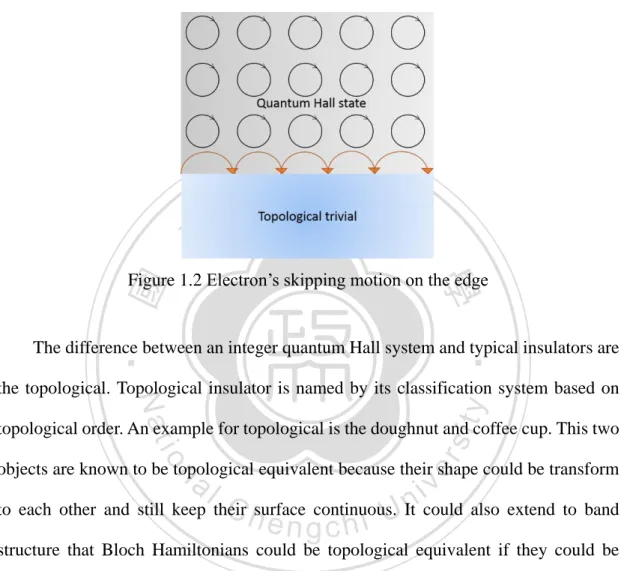
(10) All of this orbit motion corresponds to their particular energy and the energy are also got quantized. This energy levels are called Landau Levels and the energy could be determined by 1. ϵ𝑛 = ℏω𝑐 (𝑛 + ). (Equation 1-2). 2. where n is any positive integer value. Each one of Landau levels are separated with energy ℏωc . When the quantum number n is large enough, the quantum mechanical behavior would be closed to the classical behavior and this principle only suitable in ℏωc .. 政 治 大 To discuss the insulator 立case, we could imagine that the Landau Levels below the. ‧ 國. 學. Fermi level are occupied. When the Landau Levels are higher than Fermi level, they are unoccupied. And it could produce a band gap and the band structure is similar to a. ‧. typical insulator. This kind system was called integer Quantum Hall state but there is a. sit. y. Nat. difference between a typical insulator and integer Quantum Hall state. The electrons in. n. al. er. io. typical insulator are bound to atoms but the electrons are allowed to drift while applying. i n U. v. an electrical field. This electrons caused to a Hall current with Hall conductivity which was determined by. Ch. engchi σ𝑥𝑦. 𝑁𝑒 2 = ℎ. (Equation 1-3). where e is electron charge, ℎ is Planck’s constant and N is the filling factor. From this conductivity, we start linking the Integer Quantum Hall state and 2D topological insulator system. Now let’s think about a real world of the x-y plane. At the edge of the xy plane, the electrons at this area couldn’t fulfill an entire cyclotron orbit. Finally, the electrons bounce from the edge and lead a skipping motion. (Figure 1.2). The cyclotron orbit direction is dependent on the external magnetic field and carriers the skipping 4.
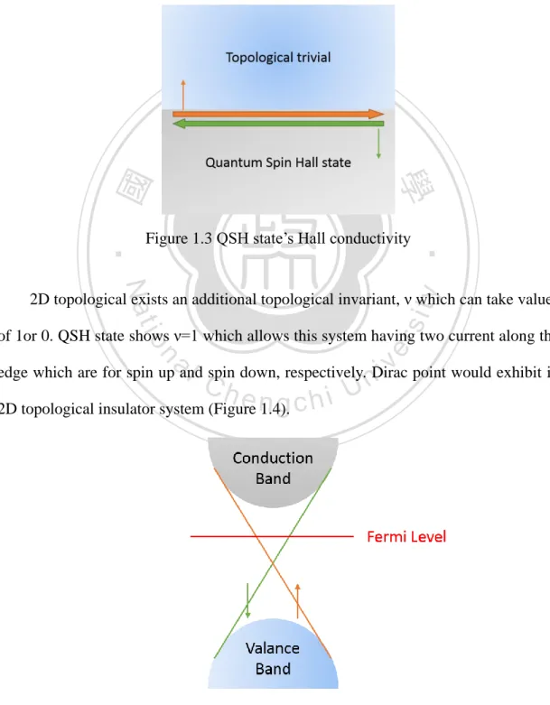
(11) motion is also fixed to only one direction along one edge. The motion is called chiral and could be presented by a band structure as a gapless state. The unidirectional conducting edges are causing to a change in topological Chern invariants which come from n=0 to n=1.. 立. 政 治 大. ‧ 國. 學. Figure 1.2 Electron’s skipping motion on the edge. ‧. The difference between an integer quantum Hall system and typical insulators are. sit. y. Nat. the topological. Topological insulator is named by its classification system based on. io. er. topological order. An example for topological is the doughnut and coffee cup. This two objects are known to be topological equivalent because their shape could be transform. al. n. v i n C hsurface continuous.U It could also extend to band to each other and still keep their engchi structure that Bloch Hamiltonians could be topological equivalent if they could be. continuously distorted into each other. The topological invariant is the characteristic to this material. We have introduced the fundamental principle of the Integer Quantum Hall state and the difference of the typical insulator. The IQH state and 2D topological have something similar. Both of them show an insulating inside the bulk but conducting on the edge which is topologically protected. 2D topological insulator’s spin degenerates are the difference of IQH state and 2D TI. Therefore, 2D topological insulator is an 5.
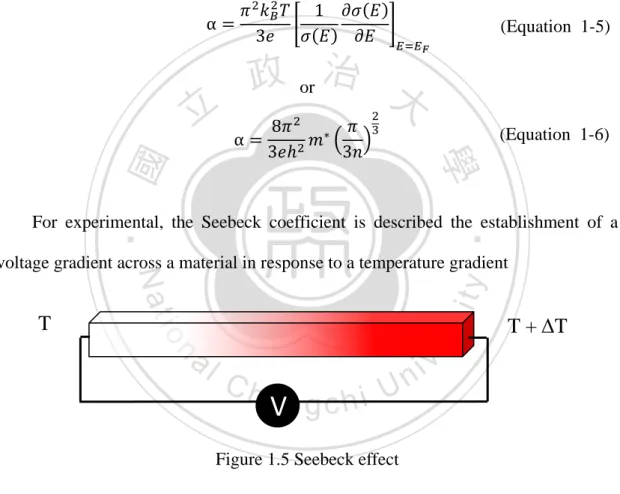
(12) example of Quantum spin Hall (QSH) state which is very familiar to Integer Quantum Hall state. The QSH state had two Hall conductivity, one comes from spin up and the other from spin down electrons, respectively (Figure 1.3). This two current values are equal but directions are opposite. It shows a zero net current but has a quantized spin Hall conductivity and Hall conductivity has its independent Chern number as n↑ and n↓ with n↑ + n↓ = 0.. 學 Figure 1.3 QSH state’s Hall conductivity. Nat. y. ‧. ‧ 國. 立. 政 治 大. sit. 2D topological exists an additional topological invariant, ν which can take values. n. al. er. io. of 1or 0. QSH state shows ν=1 which allows this system having two current along the. i n U. v. edge which are for spin up and spin down, respectively. Dirac point would exhibit in. Ch. engchi. 2D topological insulator system (Figure 1.4).. Figure 1.4 3D TI Band structure and Dirac cone 6.
(13) 1.1.2. 3D Topological Insulator. In last section, we have introduced 2D topological insulator system and some basic principle for this materials. It is an important different between Quantum Spin Hall state and a 3D topological. Both of them could have the conduction edge or surface, but the results are different. In QSH state, it have to apple an external magnetic field. However, 3D topological insulator needs not any field, it is causing to spin-orbit coupling rather than applied field. 3D TI isn’t simply stacking many 2D TI but is a brand new system. The 3D TI’s surface states are a non-trivial bulk topology effect.. 政 治 大 whether it is topological non-trivial or not. It could start from the energy level of 立. Topological invariants are determined by calculating the parity of this system. ‧ 國. 學. Bismuth (6s26p3) and Selenium (4s24p3) of time-reversal invariant points near the Fermi level. Because the electrons near to Fermi level are almost p-orbitals so we could. ‧. neglected the s-orbits electron here. First effect is that chemical bond between Bi and. sit. y. Nat. Se would concern to the state energy. Second effect is that the crystal field splitting are. io. al. n. defined by. er. affect the spin-orbital coupling. Finally, the spin-orbit coupling Hamiltonian which is. Ch. engchi. ℋ𝑆𝑂𝐶 = 𝜆𝐿 ∙ 𝑆. i n U. v. (Equation 1-4). Where L is the orbit momentum and S is the spin momentum. Spin orbital coupling would lead the level reversed and closed to Fermi energy when λ is large enough. The reversion could change the parity and could transform a trivial insulator to a non-trivial insulator.. 7.
(14) 1.2. Weak Anti Localization In this section, we would to introduce the weak anti localization which is also a. feature of topological insulator behavior. To discuss WAL effect, we would start from the weak localization and then extend to the weak anti localization. At the first, imagining a system which carriers are restricted in 2D system with no external magnetic field. Considering a disordered system, the carriers are determined by scattering events and are relative to resistivity. Think about a carrier moves from A. 政 治 大 effect should be a condition needed to be considered. As a case that is a carrier which 立 to B and could move along any different direction. At the low temperature, quantum. start at a certain point and is under lots of scattering events before it goes back to the. ‧ 國. 學. original point along a loop path in a 2D system. In time reversal symmetry system, the. ‧. probability amplitude of the carriers are defined equal weather it is clockwise or counter. sit. y. Nat. clockwise. The quantum wave function of these path would produce a constructive. io. er. interference with each other which is like a scatter in a loop and increasing the resistivity. This phenomena is defined as weak localization. In experimental could be observed the. al. n. v i n C h as a function when resistivity increasing with temperature temperature is low enough engchi U to show the quantum interference behavior.. Weak anti-localization is similar to the weak localization which essential conditions are same. The differences are that WAL describes the destructive interference between two wave function. With the spin-orbital coupling, the two wave function could cancel each other and shows a lower resistance. WAL isn’t observed a resistivity decrease as a function of temperature but magneto field could destroy time reversal symmetry causing WAL to be strong dependent on the magneto field. The results are that two wave functions couldn’t cancel each other under a magnetic field and we would observed a obvious dip in magneto-resistance around B=0. 8.
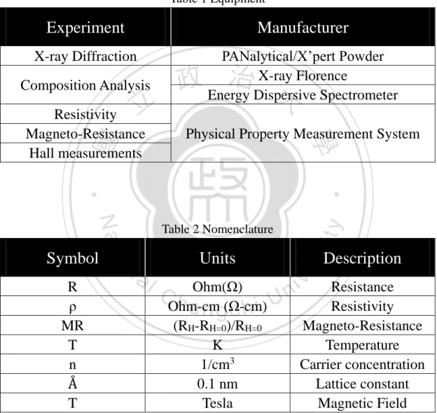
(15) 1.3. Seebeck Effect. In 1821, Seebeck effect was discovered by Baltic German physicist Thomas Johann Seebeck which is conversion of temperature differences directly into electricity. From the Mott’s formula the Seebeck coefficient was defined in. α=. 政 or 治 大. (Equation 1-5) 𝐹. 2. 8𝜋 2 ∗ 𝜋 3 α= 𝑚 ( ) 3𝑒ℎ2 3𝑛. (Equation 1-6). 學. ‧ 國. 立. 𝜋 2 𝑘𝐵2 𝑇 1 𝜕𝜎(𝐸) [ ] 3𝑒 𝜎(𝐸) 𝜕𝐸 𝐸=𝐸. ‧. For experimental, the Seebeck coefficient is described the establishment of a. y. sit. n. al. er. io. T. Nat. voltage gradient across a material in response to a temperature gradient. Ch. eVn g c h i. i n U. T + ΔT. v. Figure 1.5 Seebeck effect. Sab =. dV dT. (Equation 1-7). Where S𝑎𝑏 is the Seebeck coefficient (V/K) of of this material. Seebeck coefficient could be positive or negtive and show what kind the carriers are. Dominate carriers are electrons or holes would lead Seebeck coefficient values become are positive or negtive.. 9.
(16) Chapter 2 Experimental Techniques. 2.1. Equipment & Nomenclature. Table 1 Equipment. Experiment. Manufacturer. X-ray Diffraction. PANalytical/X’pert Powder X-ray Florence Energy Dispersive Spectrometer. Composition Analysis. 立. ‧ 國. n. al. sit. io. R ρ MR T n Å T. Units. Description. er. Table 2 Nomenclature. y. ‧. Nat Symbol. Physical Property Measurement System. 學. Resistivity Magneto-Resistance Hall measurements. 政 治 大. v Resistance i Ohm(Ω) n Ch Ohm-cm Resistivity e n g(Ω-cm) chi U (RH-RH=0)/RH=0 Magneto-Resistance K Temperature 3 1/cm Carrier concentration 0.1 nm Lattice constant Tesla Magnetic Field. 10.
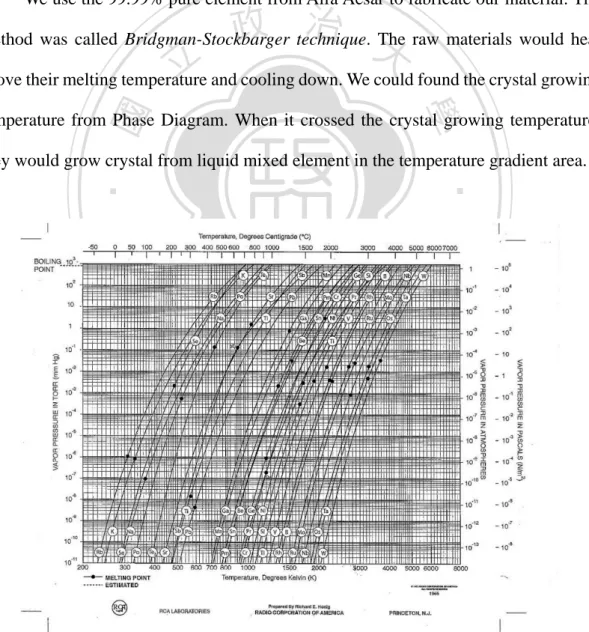
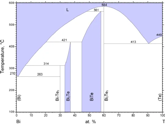
(17) 2.2. Bulk Fabrication. Prepare elements with the nominal ratio in the dry box and put into small tube. The tube was put into larger quartz tube and Zirconium foil also put into quartz tube to sorb the oxygen, and the quartz tube was sealed by helium-oxygen flame under 10-5torr. The Sealed quartz tube was placed in Aluminum oxide holder and put into furnace to fabricate with annealing pattern. We use the 99.99% pure element from Alfa Aesar to fabricate our material. The. 政 治 大. method was called Bridgman-Stockbarger technique. The raw materials would heat. 立. above their melting temperature and cooling down. We could found the crystal growing. ‧ 國. 學. temperature from Phase Diagram. When it crossed the crystal growing temperature, they would grow crystal from liquid mixed element in the temperature gradient area.. ‧. n. er. io. sit. y. Nat. al. Ch. engchi. i n U. v. Figure 2.1 (a) Vapor pressure in Pascal. 11.
(18) 立. 政 治 大. ‧. ‧ 國. 學. n. er. io. sit. y. Nat. al. Ch. engchi. i n U. Figure 2.1 (b) Phase Diagram. 12. v.
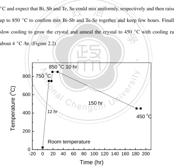
(19) To synthesize pure crystal, the first we have to know the relation about this four elements (Bi, Sb, Te, Se). The first, we have to know their melting point, and vapor pressure. Second, following phase diagram (Figure 2.1 (b)), we can know the phase we wanted will produce at which temperature, respectively. From the phase diagram we knew that the Se, Te and Bi, Sb could melt each other in any concentration. According to Figure 2.1 (a), we can see that selenium had large vapor pressure in high temperature. We first considered the Selenium effect in our process. According to the Bi-Se diagram, we could know that the Bi2Se3 grew in 705 ⁰C. We raise the temperature slowly to 750. 政 治 大 up to 850 ⁰C to confirm mix Bi-Sb and Te-Se together and keep few hours. Finally, 立. ⁰C and expect that Bi, Sb and Te, Se could mix uniformly, respectively and then raised. 學. ‧ 國. slow cooling to grow the crystal and anneal the crystal to 450 ⁰C with cooling rate. about 4 ⁰C /hr. (Figure 2.2). y. sit er. al. n. o. o. 750 C. io. Temperature ( C). ‧. Nat. 800. o. 850 C 10 hr. 600. Ch. 12 hr. 400. e n g150c hrh i. i n U. v. o. 450 C. 200. Room temperature 0 -20. 0. 20. 40. 60. 80 100 120 140 160 180 200. Time (hr) Figure 2.2 Anneal pattern. 13.
(20) 2.3. X-ray Diffraction. X-ray diffraction (XRD) is a universal method to analysis crystallographic structure of natural and manufactured materials. Our materials are also analyzed by this method. This method is based on the Bragg diffraction which is proposed by William Lawrence Bragg and William Henry Bragg in 1913 and the Bragg’s law is expressed in 2𝑑 sin 𝜃 = nλ. (Equation 2-1). 政 治 大. Where d is the distance between two nearest layer of structures, λ is the wavelength of. 立. indicated. ‧. ‧ 國. 學. n. er. io. sit. y. Nat. al. Ch. engchi. i n U. v. Picture originated from http://zh.wikipedia.org/wiki/File:BraggPlaneDiffraction.svg. First condition to make diffraction is that wave length of X-ray source should be choose similar to our lattice size. Second, when the indicated and reflect ray’s optical path difference is equal to integer times, we can get a constructive interference. This Xray pattern will be compare with reference database to confirm the lattice structure. By refinement step, we can calculate our lattice constant by powder X-ray pattern.. 14.
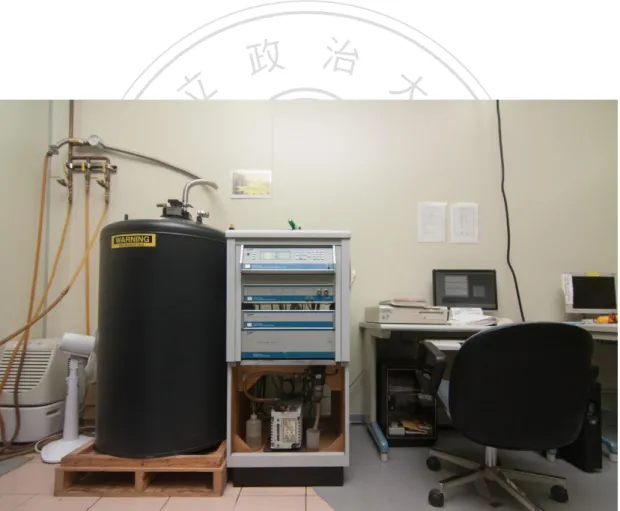
(21) 2.4. Physical property measurement system. Quantum Design - Physical property measurement system (PPMS) is an automated workstation that can perform a variety of experiments requiring precise control. We can scan temperature from 1.8-400 K with 0.2 % accuracy and applied field to ±9 T.. 立. 政 治 大. ‧. ‧ 國. 學. n. er. io. sit. y. Nat. al. Ch. engchi. i n U. v. Figure 2.3 Physical Property Measurement System. 15.
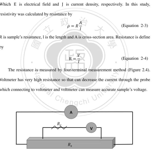
(22) 2.4.1. Resistivity. Electrical resistivity quantifies how strongly a given material opposes the flow of electric current. A low resistivity indicates a material that readily allows the movement of electric charge. In definition, the resistivity is expressed as: ρ=. 𝐸 𝐽. (Equation 2-2). Which E is electrical field and J is current density, respectively. In this study, resistivity was calculated by resistance by. 立. 𝐴 政𝜌 = 𝑅治 大 𝑙. (Equation 2-3). R is sample’s resistance, l is the length and A is cross-section area. Resistance is define. R=. 𝑉 𝐼. ‧. ‧ 國. 學. by. (Equation 2-4). sit. y. Nat. The resistance is measured by four-terminal measurement method (Figure 2.4).. io. al. er. Voltmeter has very high resistance so that can decrease the current through the probe. v. n. which connecting to voltmeter and voltmeter can measure accurate sample’s voltage.. Ch. i n U. engchi A. 𝑅𝑐. V 𝑅𝑠. Figure 2.4 Four-probe measurement. R = 𝑅𝑠 + 𝑅𝑐 , 𝑅𝑠 ≪ 𝑅𝑐 16. (Equation 2-5).
(23) The resistance would consist sample resistance and contact resistance. As an ideal case, the voltage meter has infinite large resistance. From circuitry we can know that one side resistance is great larger than the other side, the currents would flow to the small resistance side. 𝐼𝑉. 立. 政 治 大. ‧ 國. (Equation 2-6). 學. I 𝑇 = 𝐼𝑠 + 𝐼𝑐 , 𝐼𝑐 ≪ 𝐼𝑠. ‧. I 𝑇 ≈ 𝐼𝑠. (Equation 2-7). sit. y. Nat. By Equation 2-6, current flow to the voltage side is very small. The voltage from. al. er. io. contact resistance would be very small. According to following equations, we could. v. n. know that the resistance we measured is closed to the sample’s resistance.. Ch. engchi. i n U. V = 𝑉𝑠 + 𝑉𝑐 , V = 𝐼𝑅 V = 𝐼𝑠 𝑅𝑠 + 𝐼𝑐 𝑅𝑐 , V ≈ 𝐼𝑠 𝑅𝑠. R=. V 𝐼𝑠 𝑅𝑠 ≈ = 𝑅𝑠 I𝑇 𝐼𝑠. (Equation 2-8). (Equation 2-9). (Equation 2-10). After the measured resistance, we calculate resistivity by Equation 2-3. The length is defined by the ruler which is accurate to 100µm (Figure 2.6) and we take pictures with same magnification to calculate the length. 17.
(24) 2.4.2. Magneto-resistance. Magnetoresistance (MR) effect was discovered in 1856 by William Thomson, 1st Baron Kelvin. It described an electronic phenomena that resistivity is induced a variation by an external magnetic field and it was exhibit by. MR(%) =. 𝑅𝐻 − 𝑅𝐻=0 𝑅𝐻=0. (Equation 2-11). 政 治 大. Where RH=0 is non-field resistance, RH is the resistance under magnetic field.. 立. The basic magneto resistance was called Ordinary Magnetoresistance. Think about. ‧ 國. 學. electrons move with straight path. If there is an external field applied, the path would distort by Lorentz force and increasing the path. The probability of scattering would. ‧. increase, and the resistance would also increase.. y. Nat. sit. Giant magnetoresistance is a quantum mechanics effect in magnetoresistance. It. n. al. er. io. was observed in 1988 by Albert Fert and Peter Grünberg. It was observed in thin-film. i n U. v. with alternating ferromagnetic and non-magnetic conductance layer. The non-magnetic. Ch. engchi. layer would change the ferromagnetic layer’s electron conduction behavior and induce electronic scatterings which are based on the magnetic and spin orientation.. 18.
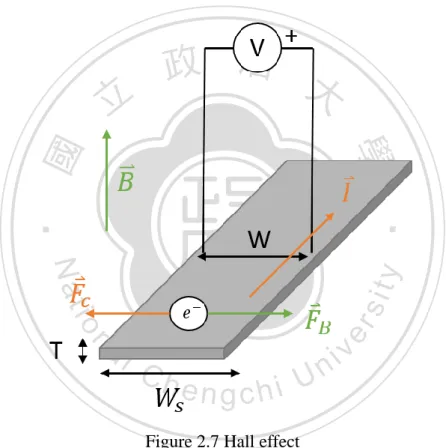
(25) 2.4.3. Hall Effect. The Hall Effect was discovered in 1879 by Edwin Herbert Hall. The Hall effect is come from the current in a conductor. The current consists lots of charge carriers. Ntype material and metal conduct with electrons and P-type material with electron holes, respectively.. 立. 政 治 大. ‧. ‧ 國. 學. n. er. io. sit. y. Nat. al. Ch. engchi. i n U. v. Figure 2.7 Hall effect. Electrons flow through a conductor and we apply an external field. The Lorentz force will push the electron to the right hand side and induce a transversal voltage call Hall voltage. ⃑⃑ × ⃑⃑⃑⃑⃑ 𝑛𝑒𝑣⃑ = 𝑗⃑ , 𝐼⃑ = 𝑗⃑ ∙ 𝐴⃑ , 𝐴⃑ = 𝑇 𝑊𝑠. 19. (Equation 2-12).
(26) According to electronic dynamics, we know that electrons would flow from lower voltage to higher voltage which was named by Coulomb force. This two force are on the opposite directions and they will get a balance situation. Carrier concentration could be calculate by following formulas. ⃑⃑ = 𝑞𝐸⃑⃑ , 𝑞𝑣⃑ × 𝐵. ⃑⃑ ⃑⃑×𝐵 𝑛𝑒𝑇𝑊𝑠 𝑣 𝑛𝑒𝑇𝑊𝑠. = 𝐸⃑⃑. (Equation 2-13). ⃑⃑ 𝐼⃑ × 𝐵 ∙ 𝑑𝑙⃑ = 𝐸⃑⃑ ∙ 𝑑𝑙⃑ = 𝑑V 𝑛𝑒𝑇𝑊𝑠 𝑛=. 立. (Equation 2-14). 𝐼𝐵 𝐵 = 𝑉𝐻 𝑒𝑇 𝑅𝐻 𝑒𝑇. (Equation 2-15). 政 治 大. ‧ 國. 學. For experimental, the voltage wire can’t perfectly connect to the edge of the sample and the theoretical equations should be calibrated to the Equation 2-17.. n. Ch. engchi U. y. (Equation 2-16). sit. 𝐼𝐵𝑊 𝑉𝐻 𝑒𝑇𝑊𝑠. er. io. al. 𝑛=. ‧. Nat. ⃑⃑ 𝐼⃑ × 𝐵 ∙ 𝑑𝑙⃑ = 𝐸⃑⃑ ∙ 𝑑𝑙⃑ = 𝑑V 𝑛𝑒𝑇𝑊𝑠. v ni. (Equation 2-17). It is easy to get resistance from PPMS data without any calculate, so we changed the Hall Voltage to Hall Resistance to make calculates simply.. 𝑛=. 𝐵 𝑊 𝑅𝐻 𝑒𝑇 𝑊𝑠. (Equation 2-18). Where, e is electron charge constant, I is current, B is magnetic field and T is the thickness. Ws and W are the width of the sample and distant between voltage wires, respectively. J is current density, A is cross-section area and n is carrier concentration. 20.
(27) M.K.S. : B(Tesla) , L(Meter), I(Ampere), V(Volt), e(Column), n(1/m3). The Hall voltage would consist magneto-resistance inside. By measurement positive and negative Hall voltage and subtract each other, we could get the exact hall voltage by following equation. 𝑉𝐻 =. 立. 1 (𝑉 + − 𝑉𝐻 − ) 2 𝐻. (Equation 2-19). 政 治 大. ‧. ‧ 國. 學. n. er. io. sit. y. Nat. al. Ch. engchi. i n U. Figure 2.8 PPMS puck. 21. v.
(28) 2.6. Composition Analysis. 2.6.1. X-ray Florence Each elements have their characteristic spectra, to analysis the spectra which has. been excited by bombarding and we can know what the element is. X-ray fluorescence (XRF) is a kind of spectra by distinguished the emission of characteristic secondary Xray from elements in the material. The light source could be high-energy X-ray or gamma rays.. 立. 政 治 大. ZSX Primus II form Rigaku was a kind of XRF commercial machine which could. ‧ 國. 學. get 5% resolution in measurement. Because of our samples are a series of concentration, they are suitably measured by the qualitative analysis. After strip the elements which. ‧. we don’t want, we can get qualitative results in weight. The mole ratio is calculating by. y. Nat. n. al. er. io. sit. atomic mass. (Figure 2.9). 2.6.2. Energy Dispersive C Spectrometer h. engchi. i n U. v. Energy Dispersive Spectrometer (EDS) is also a spectrometer which could analysis the element. The difference to XRF was the light source different. EDS uses the electron beam but the XRF uses the X-ray. The Electron beam tunneling deep is smaller than X-ray, so EDS results are skilled in surface concentration and the X-ray is good at the bulk concentration analysis. (Figure 2.10). 22.
(29) Figure 2.9 XRF-ZSX Primus II. 學. ‧ 國. 立. 政 治 大. ‧. n. er. io. sit. y. Nat. al. Ch. engchi. i n U. Figure 2.10 EDS on SEM 23. v.
(30) 2.7. Seebeck coefficient measurement. The seebeck measurement system was estabish on a coper base like figure.XXX The heater was an constant resistor with 1.5KΩ and pasted by GE vanish. The thermal couple was made by Cu and C.C. wire with about 125Ω. The heater generated heat flow from up to down, and coper base was connected to a heat sink and then establish and temperature gradient. The two thermal couple was separate connecting to the sample and Cu base.. 立. 政 治 大. ‧. ‧ 國. 學. n. er. io. sit. y. Nat. al. Ch. engchi. i n U. v. Figure 2.11 Seebeck measurement system. When the heater turned on, we could measure the VH and VL. Seebeck coefficient of thermal couple was known so we could directly calculate the temperature gradient and sample’s temperature gradient ΔT could calculate by TH-TC. Until the temperature gradient was established stable, we read the voltage from the two thermal couple. We could calculate the Seebeck coefficient by the Equation 1-7. 24.
(31) Chapter 3. 3.1. Experimental Results. Composition Analysis. 3.1.1. XRF & EDS. 政 治 大 qualitative measurement and chose the element we want to avoid noise signal in our 立. In this section, composition was measured by X-ray Florence. We use the. 學 Table 3 Element composition with XRF. Bi1.5Sb0.5Te1.4Se1.6. MF16 Bi1.5Sb0.5Te1.7Se1.3. MF19 Bi1.5Sb0.5Te1.8Se1.2. MF17 Bi1.5Sb0.5Te1.7Se1.3. al 1.54C h. sit. Sb. Te. Se. er. Bi. n. MF20. io. Sample Name. y. Nat. X-ray Florence. ‧. ‧ 國. results. Table 3 shows the results of our samples and were normalized by (Bi + Sb) = 2.. iv n 0.45 1.32 engchi U. 1.68. 1.51. 0.49. 1.62. 1.40. 1.53. 0.48. 1.74. 1.27. 1.52. 0.48. 1.70. 1.14. 25.
(32) Table 4 Element composition with EDS. Energy Dispersive Spectrometer. Bi. Sb. Te. Se. 1.53. 0.46. 1.19. 1.73. 1.44. 0.55. 1.48. 1.49. 0.52 1.50 政 治 大. 1.36. Sample Name MF20 Bi1.5Sb0.5Te1.4Se1.6. MF16 Bi1.5Sb0.5Te1.7Se1.3. MF19. 1.49. Bi1.5Sb0.5Te1.8Se1.2. 立. MF17. 1.68. 1.19. ‧. ‧ 國. 0.43. 學. 1.57. Bi1.5Sb0.5Te1.7Se1.3. In table 2 and table 3, we could see the ratio of Bi and Sb is almost 1.5: 0.5 for. Nat. sit. y. each of our samples and Selenium dopant difference could be also distinguished in this. n. al. er. io. table. According the result, we know that this crystal growing method is successful to. i n U. v. control the Selenium dopants in our material and the Bi-Sb concentration could be also. Ch. engchi. controlled. Furthermore, it also could be found that (Bi + Sb) ∶ (Te + Se) was closed to 2 ∶ 3 in each samples just in our expected.. 26.
(33) 3.1.2. X-Ray Diffraction. After the composition was analyzed, the lattice structure is determined by X-ray diffraction. For two kinds of analysis, we could observe the whole peaks with powder X-ray diffraction. And surprisingly, after we measured the bulk XRD. We found the. (015). strong characteristic peak of the rhombohedral R3𝑚 group.. 政 治 大 (110). (0123). (2110). y. (1115) (0213) (0120) (125) (128) (118). sit. (208) (1112) (0210) (2011). (202). (205). (0015) (1013). er. n. a l30. (0111). (107) (018) (0012). (104). (101). (1010). ‧(006) 國 io 20. ‧. Nat 10. 學. Intensity (a.u.). 立. 40. 50. C h Pos. [°2Th.] engchi. i n U. v. 60. 70. 80. Figure 3.1 MF19 Powder XRD pattern. We would discuss the powder XRD data. This results are come from high resolution XRD with Cu target Kα1. The whole measurements were get from 10⁰-80⁰. The target will produce Kα1 and Kα2 light source and the filter couldn’t filtrate the Kα2 light, so that the first step was strip the Kα2 signal. The second step would be subtracting the background.. 27.
(34) 立. 政 治 大. ‧ 國. 學. Figure 3.2 Powder XRD Bi2SeTe2 reference (Ref. Pattern00-029-0247). ‧. Intensity (a.u.). n. er. io. sit. y. Nat. al. MF20. Ch. engchi. i n U. v. MF16. MF19. MF17 10. 20. 30. 40. 50. 60. Pos. [°2Th.]. Figure 3.3 Powder XRD pattern 28. 70. 80.
(35) Comparing to the X-ray pattern (Figure. 3.1) and reference (Figure 3.2), it could be known that the whole peaks were come from R3𝑚 group. From the X-ray pattern the peaks were found in the reference data base. Main peak (015) was located on the about 28.5⁰. Some of wide peaks are confirmed from two or more peaks and are too close to distinguished. By the XRD analyses, there are only rhombohedral structure in our samples. Figure 3.3 shows that the different sample’s XRD peaks. It could be easily to observe that all of the patterns are the same group. The first peak (006) is observed at. 政 治 大. 18⁰, each of them get different intensity ratio. They are estimated causing by the prefer orientation.. 立. (205). (015). 40. 50. 52. v. 53. 54. 55. 60. 57. Figure 3.4 Overlap and in large Powder XRD results. (0123). (1115) (0213) (0120) (125) (128) (118) (210). 70. Pos. [°2Th.]. 29. 56. Pos. [°2Th.]. (2011). (202) (205). (110) (0111). (101). (104). (107) (018) (0012). 30. 51. (0015) (1013). 50. (0210). engchi (1010). (006). Ch. i n U. (208). al. n 20. y (208) er. sit. Intensity (a.u.). Intensity (a.u.). io 10. ‧. ‧ 國. 學. Nat. MF20 MF16 MF19 MF17. 80.
(36) Figure 3.4 has showed all this four samples’ powder XRD patterns overlap on one pattern. Each of them are normalized by the main peak intensity, which makes their main peak intensity comparatively getting the same magnitude. The black line was the zero line. It could be saw that the peaks’ comparative intensities are almost the same and almost at the same position. The right hand corner graph shows the in-large scale of this pattern of peak (205) area. The red line is high Selenium dopant and the purple line is the low dopant. In this pattern, it could be found that the peaks are shifted by the Se doped concentration. From high doping to low doping, the peaks are got shift form. 政 治 大 in the structure boundary, but are inside the structure. 立. high degree to low degree. In this analysis, it could be known that the Selenium are not. ‧. ‧ 國. 學. n. er. io. sit. y. Nat. al. Ch. engchi. 30. i n U. v.
(37) 3.1.3. Refinement. By the XRD pattern, we could qualitatively know that the structure is effected by the Selenium dopants. However, by the refinement process, we could get the quantitative results. The refinements are done by the High Score plus, it could do the refinement by semi-auto control and calculate the lattice constant. The first step is also strip Kα2 but to notice that it couldn’t subtract the background. Subtracting background process maybe leads the intensity magnitude negative which causing the refinement. 政 治 大 Figure. 3.5 shows the refinement results. We could get the lattice constant and 立. process cannot carry out.. ‧ 國. ‧ y. sit. io. 60000. n. al. er. MF16R Kawazulite 100.0 %. Nat. Counts 80000. 學. error bar.. 40000. Ch. 20000. i n U. engchi. v. 0 10. 20. 30. 40. 50 Position [°2Theta] (Copper (Cu)). Residue + Peak List. Accepted Patterns. 31. 60. 70.
(38) Counts MF17R Kawazulite 100.0 % 60000. 40000. 20000. 0 20. 30. 40. 50. 60. 70. Position [°2Theta] (Copper (Cu)). Residue + Peak List. Accepted Patterns. 政 治 大. Counts MF19R Kawazulite 100.0 %. 立. 40000. ‧. 20. 30. 40. io. 50. Accepted Patterns. Counts MF20R Kawazulite 100.0 %. 60. Position [°2Theta] (Copper (Cu)). al. n. Residue + Peak List. sit. y. Nat. 0. 70. er. 10000. ‧ 國. 20000. 學. 30000. Ch. i n U. engchi. v. 80000. 60000. 40000. 20000. 0 20. 30. 40. 50 Position [°2Theta] (Copper (Cu)). Selected Pattern: Bismuth Selenide Telluride 01-089-2007. Residue + Peak List. Accepted Patterns. Figure 3.5 Refinement results 32. 60. 70.
(39) 4.30. Bi2Te3. 30.4. Bi1.5Sb0.5Te3-ySey. 4.28. 4.26 30.0. c-axis. a,b-axis. 30.2. 4.24. 政 治 大. 立. 4.22. 29.8. 29.6. ‧ 國. 0.3 1.0. 1.1. 1.2. 1.3. 1.4. 1.5. 學. 0.0. 1.6. 1.7. Se doped concentration (y). ‧. Figure 3.6 Lattice constant. io. sit. y. Nat. n. al. er. From the refinement results, the lattice constant of a,b-axis are decreased by the. Ch. i n U. v. Selenium dopant. When the Se doping concentration is lower than 1.5, the lattice. engchi. constant decreased slightly. (Figure 3.6) We observed that lattice constant decreases sharply in Se dopant is 1.6 sample. Selenium concentration is larger than Tellurium in that sample and causing the lattice constant decreases sharply.. 33.
(40) (0021). (0018). (0015). (0012). (009). (006). Intensity (a.u.). MF20. MF16. 政 治 大. 20. MF17 30. 40. 50. 學. 60. 70. Pos. [°2Th.]. ‧ er. io. sit. Nat. Figure 3.7 Crystal surface XRD pattern. y. 10. ‧ 國. 立. MF19. al. v i n C h structure. TheU(0, 0, 3L) prefer orientation is could be indexed on the Rhombohedra engchi n. Figure 3.7 shows the XRD patterns from crystal surface, and each one of the peaks. obviously large and causing that another peaks are hard to be saw. From this pattern we could determine where the a-b plane is, and the electronic-measurements in later sections were established on the a-b plane.. 34.
(41) 3.2. Resistivity. The resistivity was measured from 2 to 300 K by standard four probe method. Figure 3.8 shows the four-terminal connecting by Platinum wire with diameter 25 µm. To decrease the contact effect, the wires are connected by wire bonding. Figure 3.9 shows the scale and for each grid was 100 µm. In this study, bulk samples length and wide are about 4 and 2 mm, respectively with thickness is about 100 µm.. 立. 政 治 大. ‧. ‧ 國. 學 er. io. sit. y. Nat Figure 3.8 Resistivity measurement. n. al. Ch. engchi. Figure 3.9 Ruler. 35. i n U. v.
(42) 100. MF20 Bi1.54Sb0.45Te1.32Se1.68 MF16 Bi1.51Sb0.49Te1.62Se1.40 MF19 Bi1.53Sb0.48Te1.74Se1.27. Resistivity (-cm). 10. MF17 Bi1.52Sb0.48Te1.70Se1.14. 1. 0.1. 0.01. 立. 100. 200. 300. 學. ‧ 國. 0. 政 治 大 Temperature (K). ‧. Figure 3.10 Temperature dependence of resistivity. n. al. 2nd Derivative. 0.1. MF20 Bi1.54Sb0.45Te1.32Se1.68. er. io. sit. y. Nat. 0.2. i n Ch Bi Sb e n gMF19 chi U. v. MF16 Bi1.51Sb0.49Te1.62Se1.40 1.53. Te1.74Se1.27. 0.48. MF17 Bi1.52Sb0.48Te1.70Se1.14. 0.0. -0.1. 0. 100. Temperature (K). Figure 3.11 Second derivative of resistivity 36.
(43) Figure 3.10 shows a temperature dependence of resistivity for different compositions. The magnitude of resistivity increases from 0.1 Ω-cm to 10 Ω-cm as temperature decrease from 300 K to 2 K, it is about 3-order increasing. It shows completely different behaviors, i.e. semiconductor behavior in 50 - 300 K and a constant at low temperatures. As the temperature below about 50 K, surface conduction behavior was dominate and the resistivity is independent on temperature. When the temperature increases beyound about 50 K, the carriers are actived by the thermal energy, and the conductivity. 政 治 大 insulator behavior. We can observe an inflection point between two kinds of resistivity 立. increases. The bulk carriers dominate in electrical conduction and shows a typical. behavior.. ‧ 國. ‧ Bi1.5Sb0.5Te3-ySey. n. al. er. io 120. sit. y. Nat. 160. RT-Inflection point (K). 學. 200. Ch. engchi. i n U. v. 80. 40. 1.1. 1.2. 1.3. 1.4. 1.5. 1.6. Y (Se doped concentration). Figure 3.12 Se concentration dependence of Resistivity inflection point. 37.
(44) To exactly get inflection point values, Figure 3.11 shows the 2nd deriavate of temperature depedent resistivity, as the second derivative curves are cross to 0 in y axis, the inflection temperatures are determined. Figure 3.12 shows the inflection point dependance to Se concentration doped. The higher Se concentration with the higher inflection temperature is observed. The details of inflection point and the carrier correlation will be discussed in the next section.. 立. 政 治 大. ‧. ‧ 國. 學. n. er. io. sit. y. Nat. al. Ch. engchi. 38. i n U. v.
(45) 3.3. Hall measurement Carrier concentration plays an important role to discuss the complicate resistivity. behavior. In this section, we will discuss hall measurements and the carrier concentration.. 政 治 大. MF19 Bi1.53Sb0.48Te1.74Se1.27. y. al. n. 0. -2. 40. er. 60. sit. MF17 Bi1.52Sb0.48Te1.70Se1.14. io. Carrier concentration (1017/cm3). MF16 Bi1.51Sb0.49Te1.62Se1.40. Nat. 2. MF20 Bi1.54Sb0.45Te1.32Se1.68. ‧. 80. Figure 3.13 Hall effect measurement. 學. ‧ 國. 立. 30. 40. Ch. engchi. 50. 60. i n U. v. 70. Temperature (K). 20. 0. 0. 100. 200. Temperature (K). Figure 3.14 Temperature dependence of Carrier concentration 39. 300.
(46) Figure 3.13 shows the hall measurement setup with 2 current wires and 2 Hall voltage wires. By applied the field, carrier would accumulate into one hand side so that we could measure the Hall voltage (VH). This kinds of material has large magnetoresistance. This results include the sum of the magneto-resistance and the Hall resistance (RH). In the positive and negative field, the Hall resistance are RH+ = RMR + RH and RH- = RMR - RH, respectively. We suppose the magneto-resistance was symmetry in field, the Hall contribution can calculate from subtracting RH+ - RH- and dividing by 2.. 政 治 大 1/cm , respectively (Figure 3.14). The main carriers are electron 立. This result shows a semiconductor behavior, the magnitude in 300 and 2 K are about 1018 and 1015. 3. which call n-type and was double checked by Seebeck measurement. The magnitude of. ‧ 國. 學. carrier concentration decrease as temperature decrease from 300 to 50 K. It can easily. ‧. correspond to resistivity increase. According this two results, we could know that the. sit. n. al. er. io. 150. y. Nat. semiconductor behavior is leaded by electron carriers.. Ch. engchi. Temperature (K). Bi1.5Sb0.5Te3-ySey. i n U. v. 100. 50. 1.1. 1.2. 1.3. 1.4. 1.5. 1.6. 1.7. Y (Se doped concentration). Figure 3.15 Se concentration dependence of Carrier concentration singular point 40.
(47) 250. 20. MF20 Hall Resistance. 10. 150. Resistance (). Resistance (). MF19 Hall resistance. 15. 200. 100. 50. 5 0 -5 -10 -15 -20. 0. -25 0. 50. 100. 150. 200. 250. 0. 300. 50. 100. 150. 200. 250. 300. Temperature (K). Temperature (K) 140. 120. 120. MF17 Hall resistance. MF16 Hall resistance. 100. 100 80. 60 40. 立. 20. -40 0. 50. 100. 60. 40. 20. 0. 學. -20. ‧ 國. 0. 政 治 大 Resistance (). Resistance (). 80. -20. 150. 200. 250. 300. -40 0. 50. 100. Temperature (K). 150. 200. 250. 300. Temperature (K). ‧. Figure 3.16 Temperature dependence of Hall resistance. io. sit. y. Nat. n. al. er. For each results, an unusual phenomenon was observed. They show singular. Ch. i n U. v. points in the carrier concentration curve. Figure 3.16 shows temperature dependence to. engchi. Hall Resistance. It can be observed that the RH is cross through the zero point. Besides, the RH results are smooth so we are not preferred to be measurement mistakes. According to Equation 2-17, we can know that carrier concentration is inverse proportion to the Hall resistance. As RH comes to zero point, the carrier concentration would diverge and bring out the singular points. To find out the reason, we started from the Hall resistance. Figure 3.16 shows the RH are cross from negative to positive. This phenomena was already published in Bi2Te2Se3 bulk. Figure. 3.17 shows an imagination electron structure. At 0 K, the dominate carriers are electron holes. Unusually, it has to be noticed that there is a donor 41.
(48) level closed to the conduction band with thermal activation energy. When the temperature raises, the donor level starts to generate electrons to the conduction band. When the electron amounts are larger than electron holes and become to dominate, it transforms to n-type material. At the meanwhile, the electron amounts are equal to holes, the RH values are zero and the carrier concentration will be diverging and becoming to a singular point.. 立. 政 治 大. ‧. ‧ 國. 學 er. io. sit. y. Nat. al. n. v i n C hof Topological insulator Figure 3.17 Band structure and donor level engchi U In the singular point area, high resolution scanning was done. As well as the resistivity’s inflection point, we also observed that singular points have correlation to Selenium concentration. In Figure 3.15, blue points showed the singular temperature dependence of the Se dopants. We could confirm that singular points are dependent to the Se doped concentration. .. 42.
(49) Carrier Concentration @2K (1015/cm3). Bi1.5Sb0.5Te3-ySey 5. 4. 3. 2 1.1. 1.2. 1.3. 1.4. 1.5. 1.6. 學. Figure 3.18 Carrier concentration at 2 K. ‧. ‧ 國. 立. 政 治 大 Y (Se doped concentration). Carrier concentration decreases as Selenium dopant decrease. As the temperature. y. Nat. io. sit. below about 50 K, carrier concentration values are constant and independent on. n. al. er. temperature which could correspond to low tempertaure resistivity behavior.. i n U. Figure. v. 3.18, it shows Selenium concentration dependence of carrier concentration at 2 K and. Ch. engchi. resistivity results also show the same trend at 2K.. Figure 3.19 shows the combination of singular points and inflection points. It could be observed that they had direct correlation between resistivity and carrier concentration. We can calculate thermal activation from resistivity by Arrhenius Law and Arrhenius function is defined by −𝐸𝑎 ) 𝑘𝐵 𝑇. σ = 𝜎0 exp(. (Equation 3-1). Where σ is conductivity, 𝐸𝑎 is thermal activation, 𝑘𝐵 is Boltzmann constant and 𝑇 is temperature. Figure 3.20 shows thermal activation is about 20-100 meV and the 43.
(50) energy gap in Bi2Te2Se was known by 300meV from published lecture. We could conjecture that thermal activation is caused from donor level and conduction band. Thermal activation is increase with Selenium dopant increase and directly effecting carrier concentration singular point. Each part of carrier concentration behaviors can correspond to different resistivity behaviors and correlation between carrier concentration and resistivity could be established.. 200. ‧ 國 1.2. n. al. 1.3. 1.4. 1.5. i n U. Se doped concnetration. Ch. engchi. er. io. sit. y. Nat. 0 1.1. ‧. 40. 學. Temperature (K). 立. 120. 80. 政 治 大. Hall Singular point RT Inflection point. 160. 1.6. v. Figure 3.19 Resistivity inflection point and Carrier singular point. 44.
(51) 140. Thermal activation (meV). 120. 100. 80. 60. 40. Bi1.5Sb0.5Te3-ySey 20 1.1. 1.2. 1.6. 1.7. ‧. al. er. sit. y. (b). n. ln (-1cm-1). 1.5. Figure 3.20 (a) Thermal activation. io. 2. 1.4. Nat. 3. 政 治 大 Y (Se doped concentration) 1.3. 學. ‧ 國. 立. (a). 1. Ch. engchi. i n U. v. 0. -1. -2 0.01. 0.02. 0.03 -1. 1/T (K ). Figure 3.20 (b) Arrhenius function fitting. 45. 0.04.
(52) 3.4. Magneto-resistance. This kind of materials have a large magneto-resistance. The magneto resistance was also measured by four-terminal method with PPMS. It was expect to observe Weak anti localization (WAL) and Shubnikov–de Haas oscillation. This two kinds phenomena could lead to analysis the surface state effect. The WAL was known from spin-orbital interaction and let it could be a spintronic material.. 立. 2800. ‧ 國. 學. 9 Tesla Zero field. ‧. 2100. sit. io. n. al. er. 1400. y. Nat. Resistance (). 政 治 大. 700. Ch. engchi. i n U. v. 0 0. 100. 200. 300. Temperature (K). Figure 3.21 Resistance at 9T and zero field. Figure. 3.21 shows the temperature dependence of resistance results under magnetic field. The MR behaviors are different in different temperature. It is observed 46.
(53) that the MR is very weak at 100 to 300 K area. At the area in 100 to 50 K, the MR started to increase. When it goes down to 2 K, the MR raises rapidly. We will discuss. MF17 Bi1.57Sb49Te1.75Se1.18. 0.2. 2K 10K 20K 50K 100K -4. 0. 4. Magnetic Field (T) 0.6. 0.0 -8. ‧ 國 4. 8. 0.2. 0.0 -8. -4. 0. Magnetic Field (T). 2K 10 K 20 K 50 K 100 K 4. 8. io. sit. Magnetic Field (T). n. er. those phenomena separately.. al. 8. 0.4. ‧. 0. 4. 學. -4. 0. Magnetic Field (T). MF20 Bi1.5Sb0.44Te1.28Se1.63. 0.6. 2K 10 K 20 K 50 K 100 K. Nat. -8. -4. 政 治 大. 立. 0.0. 2K 20K 40K 60K 80K 100K. 0.2. 8. MF19 Bi1.5Sb0.47Te1.71Se1.25. 0.3. 0.4. y. -8. Magneto-resistance (RH/R0). 0.4. 0.0. Magneto-resistance (RH/R0). MF16 Bi1.53Sb0.49Te1.60Se1.39. 0.6. Magneto-resistance (RH/R0). Magneto-resistance (RH/R0). 0.6. Ch. i n U. Figure 3.22 Magneto-resistance. engchi. v. Figure 3.22 shows the field dependence of MR with different temperature. In the 50 to 100 K, the results show a typical MR behavior which the MR is nearly proportional to B. The particular behavior was observed below 50 K and have a sharp deep. This phenomena is more obvious at low temperature, 2 K results was deliberated. At the low field area, MR increased very rapid until to about 3 tesla. This low temperature at low field MR behavior was called Weak Anti-Localization (WAL). It leads to the deep of MR in low field in this material. In publish lectures, WAL comes from the surface electron’s spin-orbital interaction and is a characteristic of 3D 47.
(54) topological insulators. When it goes to high temperature area, the bulk effects raise and cover the surface behavior. Causing that we could not observe the WAL at high temperature. Figure 3.23 shows magneto-resistance results with different composition at 2 K. We could not observe the WAL difference with different composition at low field area. At high field, different results are also getting the same value. Our explanation is that WAL doesn’t come from the bulk effect but is contributed to surface electrons so that it could be independent on Selenium dopant.. 立. 0.8. 0.6. ‧. ‧ 國. 學. MF20 MF16 MF19 MF17. sit. io. n. al. er. 0.4. y. Nat. Magneto-resistance @2K (R/R0). 政 治 大. 0.2. Ch. engchi. i n U. v. 0.0 9. 6. 3. 0. -3. Magnetic Field (Tesla). Figure 3.23 Magneto-resistance at 2K. 48. -6. -9.
(55) Chapter 4. Conclusion and Discussion. In this study, we have fabricated a series sample of Bi1.5Sb0.5Te3-ySey with y=1.1, 1.2, 1.4, 1.6 and discussed their basic physical properties. The X-ray Florence, X-ray Diffraction, Resistivity, Magneto-Resistance and Hall measurement have been done and carrier type was double checked by the Seebeck measurement. From the X-ray Florence, we could know the sample concentration difference. We. 政 治 大 would cause to different 立 results and our method could be repeatable to fabricate. have known that the same nominal concentration with difference fabrication process. ‧ 國. 學. difference concentration samples. Besides, structure analyses has been done by the Xray diffraction. Crystal surface X-ray diffraction results show the rhombohedral R3𝑚. ‧. group and prefer orientation with (0, 0, 3L) was observed. According this results, we. sit. y. Nat. could define the 𝑐̂ -axis direction and where the a-b plane is. We could make sure that. n. al. er. io. electronic analyses are based on the a-b plane. Powder X-ray Diffraction results indicate. i n U. v. that our structure is rhombohedral and the refinement processes have been done. The. Ch. engchi. lattice constant is dependent on the Selenium concentration. It was decreased with Se concentration. The magnitude of resistivity from 2 to 300 K was about 0.1 to 10 Ω-cm, respectively. In high temperature, it shows semiconductor behavior. At low temperature, resistivity values are constants and was known to be a feature of topological insulators surface conduction effect. Inflection points were observed between this two behaviors. Hall measurements provide carrier concentration information. Singular points in the carrier concentration were observed. The dominate carriers are electrons at high temperature and carrier concentration is decreasing with temperature decreasing. At 49.
(56) low temperature, dominate carrier transit to holes and the values are constant. This two behavior could correspond to resistivity results. The singular points and P-N transition are causing to active donors from donor level and thermal activation was calculated by Arrhenius law. Singular points have correlation to resistivity inflection points and the other carrier concentration behaviors could correspond to resistivity results. The magneto-resistance (MR) shows the Weak Anti Localization (WAL) at low temperature which has been demonstrated that is causing to spin-orbital interaction and a characteristic of the 3D topological insulators surface behavior. The WAL behavior. 政 治 大 Finally, the Shubnikov de Hass oscillation couldn’t be observed in magneto立. results at 2 K show that is independent on Selenium dopants.. resistance results. The reason could cause to that Fermi level is not on the Dirac cone,. ‧ 國. 學. band gap is too large or the surface is not clear enough. The future work could. ‧. synthesize samples with different Antimony dopants to change another physical. n. al. er. io. sit. y. Nat. properties and completely understand this system.. Ch. engchi. 50. i n U. v.
(57) Rference [1]. L. Fu, C. L. Kane, and E. J. Mele, Phys. Rev. Lett. 98, 106803 (2007). [2]. Z. Ren, A. A. Taskin, S. Sasaki, K. Segawa, and Y. Ando, Phys. Rev. B 82, 241306 (2010). [3]. J. S. Thakur, R. Naik, V. M. Naik, D. Haddad, G. W. Auner, J. Appl. Phys. 99, 023504 (2006). [4]. S. Sangiao, N. Marcano, J. Fan, L. Morellón, Europhys. Lett. 95, 37002 (2011). [5]. H. -T. He, G. Wang, T. Zhang, I. -K. Sou, G. K. L. Wong, Phys. Rev. Lett. 106, 166805 (2011). [6]. H. T. He, B. K. Li, H. C. Liu, X. Guo, Z. Y. Wang, Appl. Phys. Lett. 100, 032105 (2012). [7]. Y. S. Kim, M. Brahlek, N. Bansal, E. Edrey, G. A. Kapilevich, Phys. Rev. B 84, 073109 (2011). D. Hsieh, D. Qian, L. Wray, Y. Xia, Y. S. Hor, R. J. Cava, Nature (London) 452, 970 (2008). 學. [9]. ‧ 國. [8]. 政 治 大 Z. Ren, A. A. Taskin, S. Sasaki, 立 K. Segawa, and Y. Ando, Phys. Rev. B 84, 165311 (2011). [10] L. Fu and C. L. Kane, Phys. Rev. B 76, 045302 (2007). ‧. [11] M. Z. Hasan*, C. L. Kane†, Rev. Mod. Phys, Volume 82, October-December (2010). Nat. n. al. er. io. sit. y. [12] H. B. Zhang, H. L. Yu, D. H. Bao, S. W. Li, C. X. Wang , Phys. Rev. B 86, 075102 (2012). Ch. engchi. 51. i n U. v.
(58)
數據
+7
相關文件
Agent: Okay, I will issue 2 tickets for you, tomorrow 9:00 pm at AMC pacific place 11 theater, Seattle, movie ‘Deadpool’. User:
共同業務 教師成長 C/Q/S E/R/A 專業發展 C/Q/S E/R/A 實驗研究組 科學活動 C/Q/S E/R/A 研究發展 C/Q/S E/R/A 資料出版組 出版刊物 C/Q/S E/R/A 國際教育 C/Q/S
Central lab was done for toxicity check yet the sampling time is not within the allowable range as stated in protocol. Central lab data was reviewed prior to
11[] If a and b are fixed numbers, find parametric equations for the curve that consists of all possible positions of the point P in the figure, using the angle (J as the
(a) Classroom level focusing on students’ learning outcomes, in particular, information literacy (IL) and self-directed learning (SDL) as well as changes in teachers’
The non-normalizable (zero) modes picked up by the AdS/CFT description localized on the AdS boundary, which corresponds to dual CFT operators and should be topological sector of
The Liouville CFT on C g,n describes the UV region of the gauge theory, and the Seiberg-Witten (Gaiotto) curve C SW is obtained as a ramified double cover of C g,n ... ...
Thus the given improper integral is convergent and, since the integrand is positive, we can interpret the value of the integral as the area of the shaded region in Figure
