國 立 交 通 大 學
光 電 工 程 研 究 所
碩士論文
半極化面{10-11}氮化銦鎵/氮化鎵奈米金字塔
發光二極體之製作及特性研究
Fabrication and investigation of semipolar {10-11}
InGaN/GaN nanopyramid light emitting diode
研究生:陳羿蓁
指導教授:郭浩中 教授
鄒志偉 教授
國 立 交 通 大 學
光 電 工 程 研 究 所
碩士論文
半極化面{10-11}氮化銦鎵/氮化鎵奈米金字塔
發光二極體之製作及特性研究
Fabrication and investigation of semipolar {10-11}
InGaN/GaN nanopyramid light emitting diode
研究生:陳羿蓁
指導教授:郭浩中 教授
鄒志偉 教授
半極化面{10-11}氮化銦鎵/氮化鎵奈米金字塔發光二極體之
製作及特性研究
Fabrication and investigation of semipolar {10-11} InGaN/GaN
nanopyramid light emitting diode
研究生:陳羿蓁 Student:Yi-Chen Chen
指導教授:郭浩中 教授 Advisor:Hao-Chung Kuo
鄒志偉 教授 Chi-Wai Chow
國 立 交 通 大 學
光 電 工 程 研 究 所
碩 士 論 文
A Thesis
Submitted to Institute of Electro-Optical Engineering
College of Electrical Engineering
National Chiao Tung University
in Partial Fulfillment of the Requirements
for the Degree of
Master
In
Electro-Optical Engineering
July 2011
Hsinchu, Taiwan, Republic of China
中華民國一百年七月
半極化面{10-11}氮化銦鎵/氮化鎵奈米金字塔發光二極體之
製作及特性研究
研究生:陳羿蓁 指導教授:郭浩中 教授
鄒志偉 教授
國立交通大學光電工程研究所
摘要
在本論文中,我們介紹高性能綠光發光二極體用選區成長技術將半極化面 {10-11}氮化鎵奈米金字塔成長於藍寶石基板上。從穿透式電子顯微鏡(transmission electron microscopy, TEM)影像 中發現選 區成長技術可以減少半極化面{10-11}多重量子阱內的穿透錯位密度。而且,從 變功率光激發螢光(Photoluminescence, PL)量測可以看出半極化面多重量子阱的 內建電場較小、內部量子效率較高。另外,時間解析光激發螢光(Time resolved Photoluminescence, TRPL)量測顯示半極化面{10-11}多重量子阱的輻射複合時間 遠小於極化面(0001)多重量子阱。這些分析結果可以歸納出因為使用半極化面 {10-11}多重量子阱而確實能夠減緩量子阱中的量子侷限史塔克效應(Quantum confined Stark effect, QCSE)。
最後,我們將做成元件的綠光、黃綠光、橘光發光二極體用電激發螢光 (Electroluminescence, EL)量測分析出 L-I-V 曲線。此外,我們用空間解析陰極射 線 激 發 螢 光 (Cathodoluminescence, CL) 量 測 做 變 電 流 大 小 電 激 發 螢 光 (Electroluminescence, EL)量測的光譜分析討論。
Fabrication and investigation of semipolar {10-11} InGaN/GaN
nanopyramid light emitting diode
Student:Yi-Chen Chen Advisor:Hao-Chung Kuo Chi-Wai Chow
Institute of Electro-Optical Engineering
National Chiao Tung University
Abstract
In this study, we presented high performance green emission semipolar {10-11} GaN-based nanopyramid light emitting diodes (LEDs) grown on c-plane sapphire substrate by selective area epitaxy (SAE).
The transmission electron microscopy (TEM) images suggest that the SAE can suppress the threading dislocation density in the semipolar {10-11} multiple quantum well (MQWs). Besides, from power dependent PL measurement, the internal electric field (IEF) of semipolar MQWs was reduced, and the internal quantum efficiency (IQE) was improved. Moreover, time-resolved PL (TRPL) measurement shows the radiative recombination lifetime of semipolar MQWs was shorter than that of c-plane MQWs. These results could strongly confirm the reduction of quantum confined Stark effect (QCSE) by using semipolar MQWs.
Finally, the L-I-V curves of green, olivine and orange emission nanopyramid LEDs were investigated by electroluminescence (EL) measurement. And the EL peak shift and emission behavior could be referred to the spatial distribution of nanopyramid, which was investigated by by cathodoluminescence (CL) measurement.
Acknowledgements
時間流逝得很快,轉眼間兩年的碩士生涯就要結束了,在研究論文的過程中受 到了太多人太多的幫助了,如果少了你們的幫忙,就不會成就現在的我。 首先,誠摯的感謝指導教授郭浩中老師、鄒志偉老師和中研院的程育人老師, 在研究的過程中總是不厭其煩的與我討論,給了我許多有用的意見還有鼓勵,另 外,感謝老師提供良好的實驗儀器設備,使我的研究可以進行得很順利。 感謝 Epi teem 大家長李博,在咪聽的過程中教導了我們非常多的專業知識; 感謝金釵,在我有疑惑的時候總是耐心的幫我解答;感謝鏡學,不論多基礎的問 題都願意回答我;感謝 DAVID,做實驗的時候常常及時救援;感謝宅宅 Jo 博, 願意犧牲自己的休閒時間幫我改英文;感謝專業的藍博,對於實驗儀器一把罩; 感謝阿伯,CL 不知道幫我打了多少次;感謝 PM 博明學長,很認真的跟我們討 論遇到的問題;感謝聰明的哲榮,可以很快的找出問題點並提供解決的辦法;最 最最感謝詹姆世邦,這一年多來我真的學習到了很多,謝謝你給我這麼好的題目, 讓我的碩班研究之路非常充實。感謝所有幫助過我的學長姊,不論是言語上的鼓 勵或者是疑難雜症的解惑都讓我學到了很多。 感謝誠實的瑋婷,不經意的話都很有爆點,什麼心事都可以互相分享,謝謝 你回答了我很多關於 EL 的問題;感謝慢一拍 kaka,卡式風格讓我笑到肚子長 肌肉,超級好揪的跟團咖;感謝季瑾,大老遠的跑過來跟我們咪聽;感謝厲害的 昀瑾,SketchUp 大神,為難你忙碩論還要幫我趕圖;感謝少根筋 90,雖然講話 超誇張但我還是很愛聽,出去玩都麻煩你規劃路線,謝謝你充電之旅幫我那麼多 的忙;感謝正義魔人肉圓,剛到新竹人生地不熟的時候給我很多幫助,一開始的美食團也都仰仗你,謝謝你開心的接受你的外號;感謝攝影大師幼齒,每次出去 都背著很重的傢伙,有的沒的都可以亂說,謝謝你聽了我那麼多抱怨;感謝小朋 友的家齊,總是很準時抵達大家約定的地點,下次會好好保護你的,謝謝你幫我 分擔了很多 PL 的實驗;感謝愛妻小杜,大量買東西都要靠你的車,謝謝你在製 程上幫了我很多的忙;感謝大神阿 po,就算沒搞清楚狀況還是會跟團,不論如 何都會排除萬難的出現;感謝幽默的大寶,讓人無法忘記的飄逸背影,勞煩你每 次照完都還會幫大家刪除醜照;感謝優秀的阿國,很阿莎力的把禮物服裝表演一 番,沒有服裝的表演也讓大家很開心;感謝股票專家冠霖,提供了很多公司的情 報,以後變成專家別忘了幫我理財;感謝帥氣的 Just,蜂蜜牛奶超好喝的,每次 聽到讚美心情都很好;感謝美食專家 SGG,很多餐廳的資訊都知道,每次需要 換錢都很方便;感謝訓利哥,工數超級厲害,謝謝你代替大家獻花;感謝所有碩 二,謝謝大家陪我一起瘋瘋狂狂瘋瘋癲癲的四處闖蕩,讓我的碩班生涯多采多姿, 留下了非常多美好的回憶,不論何時只要想到你們都會很開心,真的很高興能夠 遇到你們,我們一定要成為永遠的朋友! 感謝超級威 Ben Sou,幫我分擔很多煩惱,不論任何軟體、實驗、模擬都難 不倒,謝謝你願意花那麼多的時間幫助我;感謝 pink 雨婷、球男哲宇,幫忙分 擔了很多量測實驗;感謝乖巧 Bush,常常麻煩你做 EL,你也都很願意幫忙;感 謝魔王,幫我做了很多製程;感謝老漢,幫我量積分球;感謝所有碩一,共同擁 有了很多在實驗室的回憶。 最後,要感謝我最親愛的家人,謝謝你們總是支持我做的決定,常常關心和鼓 勵我,讓我可以很順利的念到碩士畢業,我會永遠好愛好愛你們!
Content
摘要...i Abstract...ii Acknowledgements...iii Content...iv List of Tables...vi List of Figures...viiChapter 1 Introduction
1.1 Development of III-Nitride Light-Emitting Diodes 1.1.1 Wide bandgap III-nitride Materials………...………..11.1.2 History of GaN-based LEDs………...………....2
1.2 Nonpolar and Semipolar III-Nitride Light-Emitting Diodes: Achievements and Challenges……….4
1.3 Motivation……….8
Chapter 2 Experimental Instruments and Methods
2.1 Transmission electron microscope (TEM) ………112.2 Photoluminescence spectroscopy (PL) 2.2.1 Power dependent and temperature dependent PL……….…15
2.2.2 Time-resolved PL (TRPL) ………17
2.3 Electroluminescence spectroscopy (EL) ………20
2.4 Scanning electron microscope-Cathodoluminescence (SEM-CL)……….22
Chapter 3 Sample structure and fabrication
3.1 Fabrication of GaN nanopyramids with semipolar {10-11} InGaN/GaN MQWs……….243.2 Crystal quality analysis of the semipolar {10-11} InGaN/GaN multiple quantum
wells (MQWs) ………...………….28
3.3 Spatial resolved cathodoluminescence (CL) of nanopyramid structure……….31
Chapter 4 Optical Analysis of Polar and Semipolar MQWs
4.1 Investigation of internal electron field (IEF) 4.1.1 Introduction………...………344.1.2 Calculation………...…….…………35
4.1.3 Experimental result and discussion………...…………....40
4.2 Property of the internal quantum efficiency (IQE) 4.2.1 Theory and measurement of IQE……….………….42
4.2.2 Experimental result and discussion………...……...……….44
4.3 Carrier dynamic of multiple quantum wells (MQWs) 4.3.1 Analysis of carrier lifetime……….….….47
4.3.2 Experimental result and discussion………..…….49
Chapter 5 Electrical Property of III-nitride LED
5.1 Device performance of green nanopyramid LED…...………...………….525.2 Device performance of olivine nanopyramid LED………..……..…….59
5.3 Device performance of orange nanopyramid LED………..……..…….62
Chapter 6 Conclusion………...………….66
List of Tables
Table 1.2-1 The efficiency of 12 mil standard red, green and Blue LED at injected current 20 mA with carrier density about 2×1017 cm-3………...6 Table 4.3-1 The calculation result of 𝝉𝒓 and 𝝉𝒏𝒓 from TRPL measurement…...50
List of Figures
Figure 1.1-1 Bandgap energy versus lattice constant of III-V nitride semiconductors
at room temperature………1
Figure 1.1-2 The schematic drawing of InGaN LED………..4
Figure 1.2-1 Figure 1.2-1 The external quantum efficiency (EQE) bench mark of III-V semiconductor among visible light region………5
Figure 1.2-2 The QW structures on (a) polar and (b) nonpolar orientations and their band diagrams………....7
Figure 1.2-3 The polarization charge density as a function of tilt angle of the growth plane with respect to the c-plane in different In composition InGaN QWs………8
Figure 2.1-1 Ray diagram showing two basic operations of TEM………...12
Figure 2.2-1 Interband transitions in photoluminescence system……….13
Figure 2.2-2 The schematic of PL measurement system………..16
Figure 2.2-3 The picture of PL measurement system………...17
Figure 2.2-4 Detector signal for fluorescence detection at a pulse repetition rate of 80 MHz………18
Figure 2.2-5 Principle of TCSPC………..19
Figure 2.3-1 The schematic of EL measurement system………..21
Figure 2.3-2 The picture of EL measurement system………...22
Figure 2.4-1 Schematic diagram of a scanning electron microscope………23
Figure 3.1-1 The flow chart of nano imprint lithography (NIL)………...25
Figure 3.1-2 Illustrations of fabrication process of nanopyramid MQWs. (a) GaN template contained 1 μm undoped GaN and 1μm n-type GaN. (b) A 400 nm SiO2 layer and a 200 nm polymer layer were deposited. (c) Nanorod patterns were formed by nano imprint lithography (NIL) technique. (d) Passivated with porous SiO2 at sidewall. (e) Schematic structure of GaN-based nanorod structure with the regrowth of semipolar {10-11} GaN pyramids and 10-pair In0.3Ga0.7N/GaN (3nm/12nm) MQWs……….26
Figure 3.1-3 The angle-view SEM images of (a) GaN nanorod arraays. (b) GaN nanorod with sidewall passivation. (c) GaN nanoarrow arrays with semipolar {10-11} In0.3Ga0.7N/GaN MQW………..27 Figure 3.1-4 Illustration of nanopyramid LED device………..28 Figure 3.2-1 The TEM images of (a) GaN nanorod with semipolar nanopyramids.
(b) Enlarge view of semiolar {10-11} MQWs……….29 Figure 3.2-2 The mechanism of reduce threading dislocation density(TDD) in
semipolar {10-11} MQWs by (a) nano imprint lithography (NIL) and (b) epitaxy lateral overgrowth (ELO)………..30 Figure 3.3-1 Top view CL spectrum of semipolar MQWs………...32 Figure 3.3-2 (a) Top view SEM image. CL emission signal at fix emission
wavelength (b) 460 nm, (c) 480 nm, (d) 500 nm, (e) 520 nm,
(f) 540 nm, (g) 560 nm and (h) 580 nm, respectively………..33 Figure 4.1-1 (a) Energy band diagram of a p-n junction under exciting light.
(b) Idealized equivalent circuit……….36 Figure 4.1-2 The infinite quantum well………38 Figure 4.1-3 The PL peak emission energy with different excitation power for the
semipolar and c-plane MQWs (symbols) at T=15 K. The solid lines are the internal electron field (IEF) fitting results from Equation (4.1-13)… ………..41 Figure 4.2-1 Internal quantum efficiency (IQE) as a function of different injected
carrier density for semipolar MQWs………45 Figure 4.2-2 Internal quantum efficiency (IQE) as a function of different injected
carrier density for c-plane MQWs………45 Figure 4.2-3 The simulated energy band diagram from the internal electron field
fitting results of (a) c-plane and (b) semipolar QW, respectively……46 Figure 4.3-1 Illustration of radiative and nonradiative transition in a semiconductor.
………..48 Figure 4.3-2 The TRPL spectrum of c-plane and semipolar MQWs at low
Figure 5.1-1 (Color online) The light output power density (mW/cm2) versus forward current and current versus voltage of nanopyramid LED. Background: A photograph image taken under an injection current of 50 mA………...53 Figure 5.1-2 (a) The EL emission spectrum with different injected current at room
temperature. (b) The two peaks wavelength shift from EL spectrum….. ………..54 Figure 5.1-3 The photograph images taken under injection current of (a) 10 mA, (b) 30 mA and (c) 100 mA………...56 Figure 5.1-4 The EL spectrum under forward current of 10 mA, 30 mA and 100 mA
, respectively (solid line). The results of Gauss multiple peaks fitting (Dash line)………....57 Figure 5.1-5 The schematic diagram of nanopyramid LED under (a) very low and
(b) high injected current………...58 Figure 5.2-1 (Color online) The light output power density (mW/cm2) and forward
voltage versus forward current of nanopyramid LED. Background: An electrical luminescence image taken under injection current 50 mA ………...…………...60 Figure 5.2-2 (a) The EL emission spectrum with different injected current at room
temperature. (b) The two peaks wavelength shift from EL spectrum….. ………..61 Figure 5.3-1 (Color online) The light output power density (mW/cm2) versus
forward current and current versus voltage of nanopyramid LED. Background: A photograph image taken under an injection current of 200 mA……….62 Figure 5.3-2 (a) The EL emission spectrum with different injected current at room
temperature. (b) The two peaks wavelength shift from EL spectrum….. ………..64
Chapter 1. Introduction
1.1 Development Characteristic of III-Nitride Light-Emitting Diodes 1.1.1 Wide bandgap III-nitride Materials
The III-nitride materials have attracted much attention due to its tremendous potential for fabricating light emitting diodes (LEDs) with a full color application. The bandgap of the wurtzite polytypes of III-nitrides material cover a very wide range, from 0.7 eV for InN to 6.1 eV for AlN, which represents the emission wavelength from infrared (IR) region to deep ultraviolet (UV). Figure 1.1-1 shows the bandgaps of various alloys of III-Nitrides [1].
Figure 1.1-1 Bandgap energy versus lattice constant of III-V nitride semiconductors at room temperature.
With such wide emission wavelength range, III-nitrides materials is promising for applying in the applications of optoelectronic devices such as flat panel display, competing storage technologies, automobiles, general lighting and biotechnology, and so on [2-4].
With some unique properties, the III-nitride semiconductor material is not only suitable for lighting source in short wavelength in visible region but also high-speed/high-power electron device [5]. For instance, it has high bond energy (~2.3 eV), high-saturation velocity (~2.7 × 104 cm/s), high-breakdown field (~2 × 10⁶ V/cm), and strong excitonic effects (>50 meV) [6-7].
Although III-nitride semiconductors are suitable for applying in high efficiency lighting devices, they also have some inherent drawbacks to deteriorate the lighting efficiency like internal piezoelectric field and spontaneous polarization at heterointerface leading to the quantum confined Stark effect (QCSE) and causing charge separation between electrons and holes in quantum wells [8-9]. Even though, it is still worth to devote more effort to overcome such problems for its great potential in solid state lighting and some groups had indeed succeeded in solving parts of this problems.
1.1.2 History of GaN-based LEDs
Light Emitting Diodes (LEDs) are solid state devices which emit light when electrical current passes through them. In LEDs made of semiconductors, the color of
the light depends on the bandgap of the semiconductor material, proceeding from red through orange, yellow, green, blue and violet as the gap increases.
The first blue light-emitting diode (LED) using III-Nitrides materials was fabricated by J. I. Pankove et al. [10] with an metal-i-n structure in 1972. Since that, related research is going on continually. However, progresses have been limited because of highly background n-type concentration resulting from the native defects commonly thought to be nitrogen vacancies and residual impurities such as Si and oxygen acted as an efficient donor, poorly conducting p-type GaN, and the lack of appropriate substrates for epitaxial growth. Until late 1980s, H. Amano et al. [11, 12] discovered a very useful application of a low-temperature buffer layer and developed low-energy electron beam interaction (LEEBI) techniques to obtain better GaN epilayer and conductive p-type GaN, initiated a new strong interest in this research field. Finally, the first GaN-based blue LED constructed of a real p-n junction was achieved, which had greatly improved in the device performance. However, the acceptor concentration of p-type GaN is still too low such that the application of these materials is still unreliable. After that, in 1992, S. Nakamura et al. [13] achieved better conductive p-type GaN material by introducing a simple thermal annealing procedure in nitrogen ambient (≧ 750 ℃). Afterward Nakamura and Mukai [14] succeeded in growing high-quality InGaN films that emitted strong band-to-band emission from green to UV by changing the indium content of InGaN with a two-flow MOCVD method. Nowadays, Most of III-Nitride based light emitting devices uses InGaN as
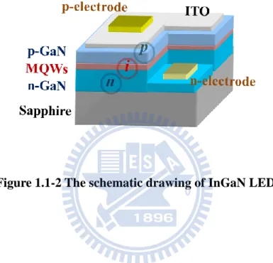
active layer instead of GaN because the difficulty of fabricating high efficiency GaN based light emitting devices. Adding a small amount of indium into the GaN is very important to obtain a strong band-to-band emission at RT. The based design of GaN LEDs is shown in Figure 1.1-2.
Figure 1.1-2 The schematic drawing of InGaN LED.
1.2 Nonpolar and Semipolar III-Nitride Light-Emitting Diodes: Achievements and Challenges
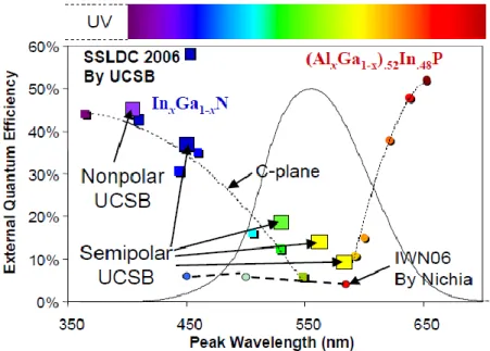
Current commercially available III-nitride based optoelectronic devices typically consist of epitaxial multilayer thin films grown along the polar c direction of the würtzite crystal structure. As the spectral range of light emission was extended from blue to green or red, we encountered a problem in luminescence efficiency (Figure 1.2-1).
Figure 1.2-1 The external quantum efficiency (EQE) bench mark of III-V semiconductor among visible light region.
Figure 1.2-1 shows the external quantum efficiency (EQE) bench mark with
different emission peak wavelength. The EQE drastically decreases from UV to green and from red to green, which is so-called efficiency green gap. There are many factors have effect on EQE from fabrication flow chart of LED:
𝜼𝑬𝑸𝑬 = 𝜼𝑰𝑸𝑬× 𝜼𝑬𝒙𝒕× 𝜼𝑬𝒍𝒆𝒄𝒕 (1.2-1) where 𝜼𝑬𝑸𝑬 is the EQE, 𝜼𝑰𝑸𝑬 is the internal quantum efficiency (IQE), 𝜼𝑬𝒙𝒕 is the light extraction efficiency, 𝜼𝑬𝒍𝒆𝒄𝒕 is the electrical loss.
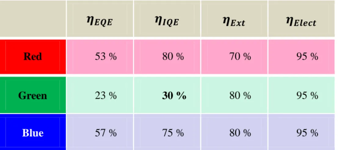
Table 1.2.1 shows the standard red, green and blue LEDs efficiency of 12 mil
chip size at injected current 20 mA with carrier density about 2×1017 cm-3. If the IQE of green LED could be improved the realization of full collar LED is very promising.
𝜼
𝑬𝑸𝑬𝜼
𝑰𝑸𝑬𝜼
𝑬𝒙𝒕𝜼
𝑬𝒍𝒆𝒄𝒕Red 53 % 80 % 70 % 95 %
Green 23 % 30 % 80 % 95 %
Blue 57 % 75 % 80 % 95 %
Table 1.2-1 The efficiency of 12 mil standard red, green and Blue LED at injected current 20 mA with carrier density about 2×1017 cm-3.
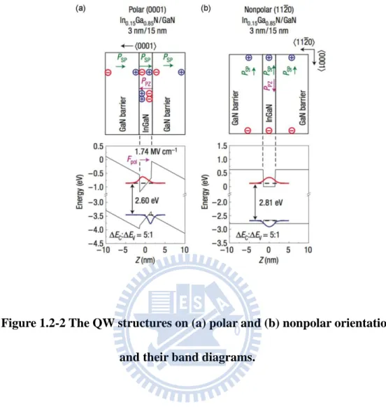
As has been reported [15], due to the strong polarization field caused by the strained InGaN layer in the c-plane, the Quantum Confined Stark Effect (QCSE) is induced which distort the energy band diagram. Therefore, it reduce the wave function overlap between the electron and hole as well as the radiative recombination. Moreover, the large blueshift of peak emission wavelength with increasing bias due to the carrier-induced screening of the polarization field could be observed.
To eliminate these polarization effects, growing devices on the nonpolar plane has been demonstrated. Figure 1.2-2 shows the stimulation band diagram of polar and nonpolar QWs [16].
Figure 1.2-2 The QW structures on (a) polar and (b) nonpolar orientations and their band diagrams.
In 2006, Romanov et al. [17] calculated polarization charge density in InGaN QWs as a function of tilt angle of the growth plane with respect to the c-plane (Figure
1.2-3). Notice that semipolar planes provide a reasonable approach to reduce the
polarization field. For blue or green LEDs, UCSB has already used nonpolar m-plnae and semipolar {10-11} GaN substrate to enhance the EQE (Figure 1.2-1).
Figure 1.2-3 The polarization charge density as a function of tilt angle of the growth plane with respect to the c-plane in different In composition InGaN QWs.
1.3 Motivation
To date, tremendous efforts have been made to solve QCSE obstacle by using the nonpolar InGaN/GaN structure grown on various substrates [18]. However, the heteroepitaxy of nonpolar GaN still suffers from highly threading dislocation density (TDD), and the ideal solutions for the green efficiency gap is still lacking [18-19]. GaN based nanorod LEDs is an attractive approach towards achieving high efficiency LEDs [20-22].
GaN based nanorod LEDs possess lower extended defect, accommodate the large lattice mismatch between sapphire substrate and GaN epilayer [23-25], and highly light extraction structure properties [20-21].
The nano-fabrication technology can attract such considerable interest and be widely used in optoelectronic and electronic devices because it has large different optical and electrical properties with those in the bulk materials. It is also reported that nano-fabrication technology device had great potential for better quantum confinement and strain relaxation effect [26].
GaN nanorods technology is one of the famous nano-structure which has been produced by various fabrication methods. In 1997, Han et al. first proposed synthesizing GaN nanorods by using carbon nanotubes as templates [27]. The dimension of the synthesized GaN nanorods could be up to 25 μm in length and ranging from 4 to 50 μm in diameter. However, it is not a simple method for produce GaN nanorods.
The growth of single-crystal GaN nanorods by hybrid vapor-phase epitaxy [28] has been developed by Kim et al. A mask-free simple process by inductively coupled plasma-reactive ion etching (ICP-RIE) dry etching to fabricate GaN nanorods was proposed by Yu et al. [29]. The growth of GaN nanorods by using ferrocene as the catalyst, so-called vapor–liquid–solid (VLS) mechanism, was also demonstrated [30]. Fabrication of GaN nanorods by e-beam patterning and ICP etching was proposed by Chen et al. [31].
With the rapid development of the nano-structure fabrication techniques, these technologies had also been used in GaN devices. Johnson et. al demonstrated a single GaN nanowire lasing phenomenon in [32]. It is the first demonstration of single GaN
nanowire laser. Han et. al. performed the photoconduction studies on GaN nanowire transistors under UV and polarized UV illumination in 2004 [33]. Besides, Kim et. al. demonstrated a high brightness LEDs by fabricating high quality, dislocation-free InGaN/GaN nanorods [34]. In 2006, Son et. al. demonstrated a UV photodetector by using a single GaN nanorod with p-n junction [35]. With the following literatures, we could know that GaN nano-stucture have played an important role in optoelectronic and electronic devices, such as laser, LED and photo detector.
We choose nano imprint lithography (NIL) technique to form the nanorod structure [36]. And Semipolar {10-11} nanopyrimids will generate by using a combination of selective area growth (SAG).
The nano-pyramidal geometry on GaN nanorod which the InGan/GaN QWs are placed promotes significantly greater strain relaxation in the InGaN layer and combines the epitaxial lateral overgrowth (ELO) technique to eliminate the TDs [37]. From our previous report, the internal electric field (IEF) of MQWs which grown on {10-11} surface was much smaller than on conventional c-plane and the radiative recombination rate also became much faster [38-39]. It implies that semipolar {10-11} plane has a great potential as a growth surface to develop high indium composition LEDs and overcome the efficiency green gap of III-nitride light-emitting diodes. In this work, we report the electrical characterization and optical performance of green, olivine and orange emission of {10-11} semipolar nanopyramid LED on GaN nanopillar arrays.
Chapter 2. Experimental Instruments and Methods
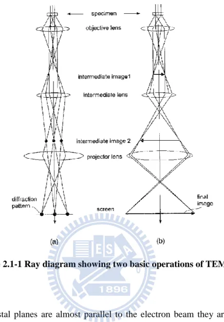
2.1 Transmission electron microscope (TEM)
TEM is a method of imaging where a beam of electrons are directed through a sample after which they are scattered into discrete diffracted beams. The diffracted electron beams are then focused in the back focal plane of the objective lens. TEM may have two modes. When operated in diffraction mode, the diffraction lens is focused on the back focal plane to produce a diffraction pattern. For the imaging mode, the diffraction lens is focused on the first image plane to produce a magnified image. In addition, the beam may be allowed to pass through the sample to obtain a bright-field image however the diffracted beams produce a dark-field image.
The ray diagram (Figure 2.1-1) shows (a) imaging projecting a diffraction pattern and (b) projection of an image onto a viewing screen. The interaction of the electron beam with crystalline material tends to be by diffraction. The orientation of the planes of atoms in the crystal to the electron beam changes the intensity of diffraction. TEM equipment often uses a goniometer to allow the sample to be tilted to a range of angles to obtain specific diffraction conditions. Diffracted electrons are also selected using different apertures. The intensity of diffraction is a maximum at the Bragg angle, although a variation of diffraction intensity occurs with deviation from the Bragg angle. This also depends on the thickness of the specimen. The thinner the crystal sample, the further the crystal may deviate from the Bragg condition.
Figure 2.1-1 Ray diagram showing two basic operations of TEM.
When crystal planes are almost parallel to the electron beam they are close to fulfilling Bragg’s Law. The majority of electrons are diffracted when the electron beam strikes one set of lattice planes exactly at their Bragg angle and only a few will pass through the sample undeviated. If the planes are exactly at the Bragg condition, strong diffraction will occur and the bright field image will appear dark. This variation with diffraction is shown with bend contours which are a feature of bending of the crystal planes. Dark contour images correspond to regions at the Bragg angle, while light contours result in the regions not strongly diffracting.
2.2 Photoluminescence spectroscopy (PL)
Photoluminescence characterization equipment generally uses the PL method to obtain the wavelength and intensity of the semiconductor material being analyzed. PL is the process of optical absorption of electrons in solids between an initial energy state Ei and a final energy state Ef. Excitation of an electron to Ef will leave Ei
unoccupied creating a hole. Absorption creates electron-hole pairs while luminescence is the process which occurs when electrons in excited states drop to a lower level emitting a photon ℏ𝝎 as shown in Figure 2.2-1. The electron–hole recombination creates a photon which is also known as a radiative transition. Direct gap materials are good light emitters and their optical properties are analyzed using this technique.
k k = 0 Valence band Conduction band ħ Eg ħ L E L
Figure 2.2-1 Interband transitions in photoluminescence system.
Photons are absorbed using an excitation source which is typically a laser. The frequency of the source ℏ𝝎𝑳 must be greater than the energy gap Eg. The result is
that electrons are injected into the conduction band and holes into the valence band. Electrons and holes are initially created in higher states within these bands but will rapidly relax to the bottom of their respective bands reaching their lowest energy state. Relaxation occurs by emitting phonons, for energy loses from the higher states, which obeys the conservation laws. The difference in energy between the two bands is
Eg which is the energy gap, also known as the band gap. Luminescence occurs close
to the band gap Eg, near k = 0. After excitation, both electrons and holes relax to their
lowest energy states by emitting phonons.
PL spectroscopy has been used as a measurement method to detect the optical properties of the materials because of its nondestructive characteristics. PL is the emission of light from a material under optical excitation. The laser light source used to excite carriers should have larger energy band gap than the semiconductors. When the laser light is absorbed within the semiconductors, it would excite the carriers from the valence band to the conduction band. Then, it produces the electrons in the conduction band and the holes in the valence band. When the electron in an excited state return to the initial state, it will emit a photon whose energy is equal to the energy difference between the excited state and the initial state, therefore, we can observed the emission peak from PL spectrum.
The photoluminescence spectroscopy is the optical measurement to examine the quality and optical characteristic of material. First, when we analysis a new compound semiconductor, we can use PL measurement to know the band gap of the new material.
Second, the intensity of PL signal is contributed to the amount of radiative recombination in the materials. Therefore, PL measurement can be used to understand the material quality and the recombination mechanisms of the materials.
The carrier recombination processes occur in many ways in order to reach the equilibrium. Those processes can be divided into radiative recombination and nonradiative recombination. We can recognize the radiative recombination easily at low temperature by PL measurement, since it would not be influenced by the thermal energy. If there are some defect energy level existed in energy band gap of semiconductor, they could also contribute to radiative recombination process. Therefore, we could observe the multiple emission peaks in the PL spectrum, and the intensity of the emission peaks is related to the contribution of the individual radiative recombination process.
2.2.1 Power dependent and temperature dependent PL
For excitation power and temperature dependent PL measurement, the laser source used in this research is femto-second-pulse Ti:sapphire. The output laser wavelength could be tuned to be around 760-820 nm by adjusting the internal resonant length and gain profile. A frequency doubler and tripler crystal is setup at the laser output optical path. Here, we adopted the doubler crystal to have a wavelength at around 380-410 nm could be obtained. It is specifically important in avoiding the absorption of GaN material itself and ensured most of the injected laser photons could
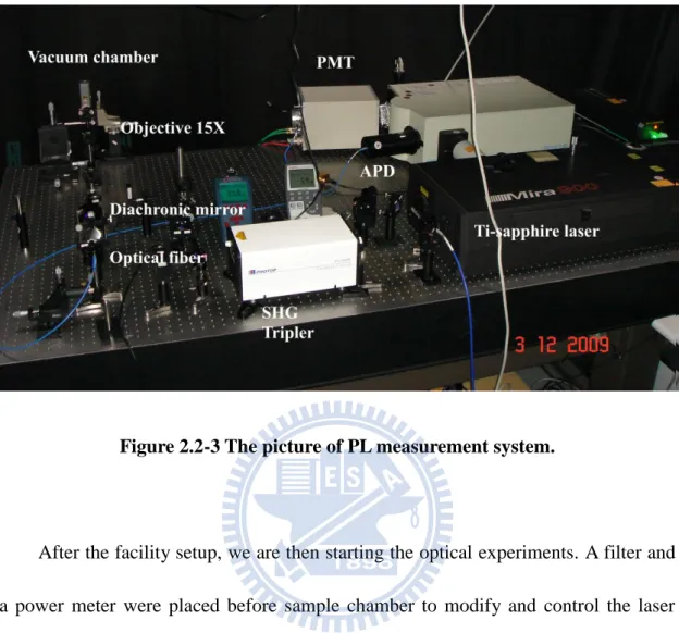
excited the photons inside the MQWs. We note that this assumption essential while we predicted the injected carrier density. The tuned the 380-410 nm laser was then incident into the sample surface vertically. The sample was mounted in a closed-cycle He cryostate with a temperature controller which could be precisely controlled in the temperature region around 15 to 300 K. By the temperature controller with a set of wire heater, we could perform a serious of temperature-dependent experiments from 15 to 300 K. The luminescence signal dispersed through a 0.55-meter monochromator was detected by the photomultiplier tube (PMT). The setup detail of temperature dependent PL is shown in Figure 2.2-2 and Figure 2.2-3.
Figure 2.2-3 The picture of PL measurement system.
After the facility setup, we are then starting the optical experiments. A filter and a power meter were placed before sample chamber to modify and control the laser output power. By rotating the filter, we could vary the excitation power changing from 5x10⁻³ mW to 80 mW.
2.2.2 Time-resolved PL (TRPL)
For TRPL measurement, the laser source was same as for excitation power and temperature dependent PL measurement, which delivers ~150 fs laser pulses at the repetition rate of 76 MHz. And use time-correlated single photon counting (TCSPC) to calculate carrier lifetime.
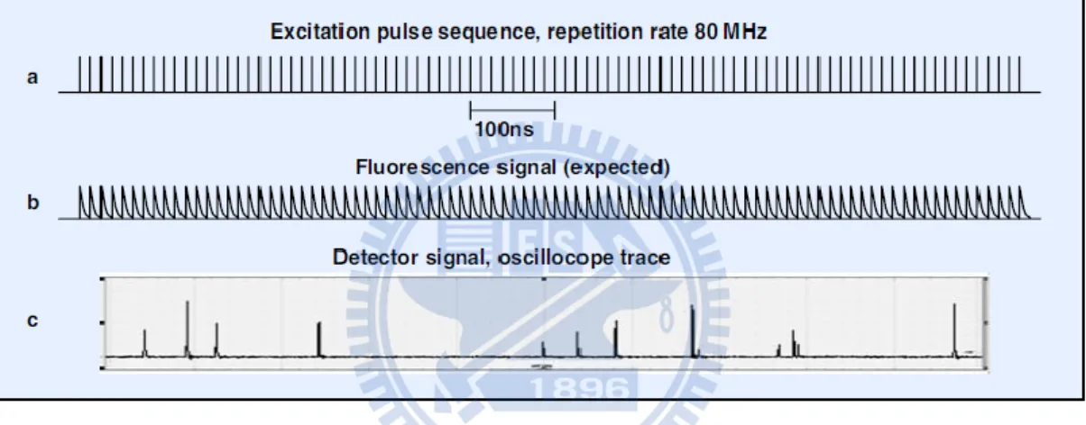
TCSPC is based on the detection of single photons of a periodic light signal, the measurement of the detection times, and the reconstruction of the waveform from the individual time measurements [40-43]. TCSPC makes use of the fact that for low-level, high-repetition rate signals the light intensity is usually low enough that the probability to detect more than one photon in one signal period is negligible. The situation is illustrated in Figure 2.2-4.
Figure 2.2-4 Detector signal for fluorescence detection at a pulse repetition rate of 80 MHz.
Fluorescence of a sample is excited by a laser of 80 MHz pulse repetition rate (a). The expected fluorescence waveform is (b). However, the detector signal measured by an oscilloscope has no similarity with the expected fluorescence waveform. Instead, it consists of a few pulses randomly spread over the time axis (c). The pulses represent the detection of single photons of the fluorescence signal. Please note that the photon detection rate of (c) is about 107 s-1, which is on the order of the maximum possible detection rate of most detectors. Thus, the fluorescence waveform (c) has to be
considered a probability distribution of the photons, not anything like a signal waveform. Moreover, Fig. 21 shows clearly that the detection of a photon in a particular signal period is a relatively unlikely event. The detection of several photons in one signal period is even less likely. TCSPC therefore neglects the detection of several photons per signal period. The principle is shown in Figure 2.2-5.
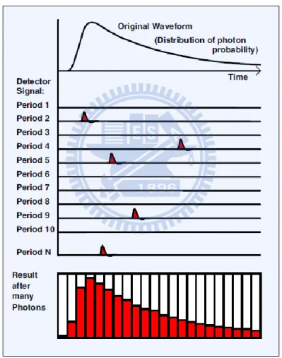
Figure 2.2-5 Principle of TCSPC.
As shown above in Figure 2.2-4, the detector signal consists of a train of randomly distributed pulses corresponding to the detection of the individual photons.
There are many signal periods without photons, other signal periods contain one photon pulse.
When a photon is detected, the arrival time of the corresponding detector pulse in the signal period is measured. The events are collected in a memory by adding a ‘1’ in a memory location with an address proportional to the detection time. After many signal periods a large number of photons has been detected, and the distribution of the photons over the time in the signal period builds up. The result represents the ‘waveform’ of the optical pulse. (Please note that there is actually no such waveform, only a distribution of the photon probability, see Figure 2.2-4.) The setup detail of TRPL is shown in Figure 2.2-2.
2.3 Electroluminescence spectroscopy (EL)
Electroluminescence (EL) is an optical phenomenon and electrical phenomenon in which a material emits light in response to an electric current passed through it, or to a strong electric field. This is distinct from light emission resulting from heat (incandescence), chemical reaction (chemiluminescence), sound (sonoluminescence), or other mechanical action (mechanoluminescence).
Electroluminescence is the result of radiative recombination of electrons and holes in a material (usually a semiconductor). The excited electrons release their energy as photons - light. Prior to recombination, electrons and holes are separated either as a result of doping of the material to form a p-n junction (in semiconductor
electroluminescent devices such as LEDs), or through excitation by impact of high-energy electrons accelerated by a strong electric field (as with the phosphors in electroluminescent displays).
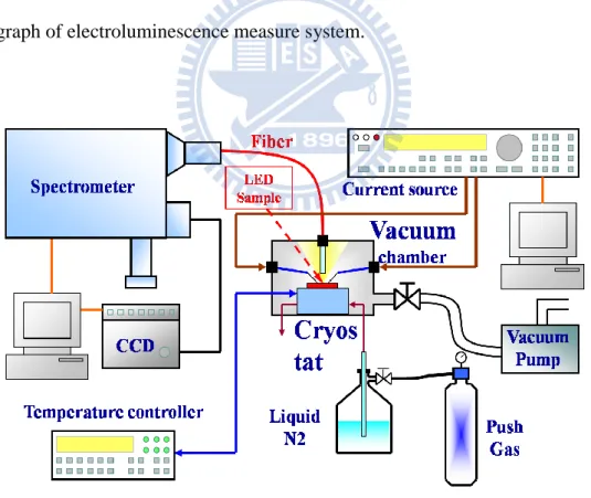
Figure 2.3-1 shows the schematic of electroluminescence measurement systems.
A set of instruments including CW current source Kiethley 238, a microscope to observe the patterned electrode of sample surface, three axial stages for probe and fiber to detected the light output, and then the light detected by a 0.32 m monochromator (Jobin-Yvon Triax-320) with 1800, 1200, and 300 grooves/mm grating and the maximum width if the entrance slit was 1 mm. Figure 2.3-2 shows the photograph of electroluminescence measure system.
Figure 2.3-2 The picture of EL measurement system.
2.4 Scanning Electron Microsope-Cathodoluminescence (SEM-CL)
The electron microscope uses electromagnetic lenses to focus the beam to produce an image. However, SEM and TEM differ in the way images are produced and magnified. SEM is used to view the surface or near surface of a sample, whereas TEM provides information of the internal structure of thin specimens. The scanning electron microscope as the name suggests scans across the specimen by the scan coils.
As the sample is scanned by the electron beam as shown in Figure 2.4-1, it emits electrons and electromagnetic radiation. A detector counts the low energy secondary electrons (< 50 eV) or other radiation emitted. The image is produced by two
dimensional intensity distributions by scanning a cathode ray tube (CRT) spot onto a screen and modulating the brightness by the amplified current from the detector. Three dimensional samples change the way electrons are emitted and results in the appearance of a three dimensional image. Resolutions less than 1 nm may be achieved.
Chapter 3. Sample structure and fabrication
In this chapter, we illustrate the fabrication flow charts of semipolar {10-11} nanopyramids LED. Moreover, the Crystalline quality analysis will be discussed by transmission electron microscope (TEM) measurement.
3.1 Fabrication of GaN nanopyramids with semipolar {10-11} InGaN/GaN MQWs
The GaN-based material was grown by a low pressure Metal-Organic Chemical Vapor Deposition (MOCVD) system. A 2 μm thick GaN layer was first grown on a 2-inch C-plane (0001) sapphire substrate. The GaN contained 1 μm undoped GaN and 1μm n-type GaN and were grown at 1150℃ and 1160℃, respectively.
The nanorod patterns were formed by nano imprint lithography (NIL) technique. First, a 400 nm SiO2 layer and a 200 nm polymer layer were deposited as the masks
during the process. Then a patterned mold was placed onto the dried polymer film. Under a high pressure, the substrate was heated over the glass transition temperature (Tg) of the polymer. After that, the substrate and the mold were cooled down to room
temperature to release the mold. After generating narorod patterns on the polymer layer, the patterns were then transferred into SiO2 layer by reactive ion etching (RIE)
with CHF3/O2 mixture, and into GaN layer by inductively coupled plasma etching (ICP) with Cl2/Ar mixture. The mask layers were removed at the end of processes.
(ICP) with Cl2/Ar mixture. The mask layers were removed at the end of processes.
Figure 3.1-1 shown the flow chart of nano imprint lithography (NIL).
Figure 3.1-1 The flow chart of nano imprint lithography (NIL).
Before the regrowth process, the sample was passivated with porous SiO2 at
sidewall. The pyramid shape n-type GaN structures were regrowth on the top of GaN nanopillars at 730℃ by using a combination of selective area growth (SAG). The 450 nm height pyramids contain 10-pair In0.3Ga0.7N/GaN (3nm/8nm) multiple quantum
wells (MQWs), which support the emission around 500 nm wavelength. The fabrication procedure was shown in Figure 3.1-2.
Figure 3.1-2 Illustrations of fabrication process of nanopyramid MQWs. (a) GaN
template contained 1 μm undoped GaN and 1μm n-type GaN. (b) A 400 nm SiO2
layer and a 200 nm polymer layer were deposited. (c) Nanorod patterns were formed by nano imprint lithography (NIL) technique. (d) Passivated with porous
SiO2 at sidewall. (e) Schematic structure of GaN-based nanorod structure with
the regrowth of semipolar {10-11} GaN pyramids and 10-pair In0.3Ga0.7N/GaN
(3nm/12nm) MQWs.
(a) (b)
(c) (d)
The diameter and the pitch of GaN nanorod was 350 nm and 750 nm, respectively. And the etch depth of the nanopillars is approximately 1 μm. Figure
3.1-3 shows the angle-view SEM images of (a) GaN nanorod. (b) GaN nanorod with
sidewall passivation. (c) GaN nanopyramids with semipolar {10-11} In0.3Ga0.7N/GaN
MQW.
Figure 3.1-3 The angle-view SEM images of (a) GaN nanorod arraays. (b) GaN nanorod with sidewall passivation. (c) GaN nanoarrow arrays with
semipolar {10-11} In0.3Ga0.7N/GaN MQW.
(c)
(b) (a)
Finally, the complete epitaxial structure then underwent a standard four-mask LED fabrication processing with ITO current spreading layer and Ni/Au contact metal depositions, into an LED structure with a mesa size of 300×300 μm2. Figure 3.1-4 shows the illustration of nanopyramid LED device.
Figure 3.1-4 Illustration of nanopyramid LED device.
3.2 Crystal quality analysis of the semipolar {10-11} InGaN/GaN multiple quantum wells (MQWs)
The TEM measurement was used to confirm the quality of semipolr {10-11} MQWs (Figure 3.2-1). The angle between the MQWs and c-plane was 62°, and the inclined surface was the semipolar {10-11} facet. There existed air voids around GaN
nanorods can act as waveguides that improve light extraction [44]. Figure 3.2-1 (b) shown TEM enlarge view of semiolar {10-11} MQWs. The interface of MQWs was smooth and the thickness of InGaN well and GaN barrier from apex to bottom of the nanopyramid were nearly uniform, which were 2 and 8 nm, respectively.
Figure 3.2-1 The TEM images of (a) GaN nanorod with semipolar nanopyramids. (b) Enlarge view of semiolar {10-11} MQWs.
The mechanism of reduce threading dislocation density (TDD) in semipolar {10-11} MQWs was shown in Figure 3.2-2. First, threading dislocations in bulk c-GaN were suppressed by nano imprint lithography (NIL). Moreover, threading dislocation was bended by epitaxy lateral overgrowth (ELO) process. Finally,
reduction of threading dislocation density (TDD) in MQWs can be observed in
Figure 3.2-1.
(a)
(b)
Figure 3.2-2 The mechanism of reduce threading dislocation density (TDD) in semipolar {10-11} MQWs by (a) nano imprint lithography (NIL) and (b) epitaxy
From the result of TEM measurement, the SAE is a promising technique to fabricate high crystalline quality semipolar {10-11} MQWs.
3.3 Spatial resolved cathodoluminescence (CL) of nanopyramid structure
To investigate the Indium content distribution on the nanoryramids surface, the scanning electron microscope (SEM) and spatial resolved cathodoluminescence (CL) measurement was applied.
Figure 3.3-2 (a) shows the top view SEM image of the semipolar MQWs. The
diameter of GaN nanopyramid is around 300 nm. And the CL spectrum was shown in
Figure 3.3-1. To investigate the spatial distribution of emission wavelength, we
collected the emission signal at fixed emission wavelength, which were 460, 480, 500, 520, 540, 560 and 580 nm, respectively (Figure 3.3-2 (b)~(h)). The peak emission wavelength at about 500 nm, corresponding to the PL measurement, came from the sidewall facets of pyramids. As shown in the figures, the emission wavelength became longer from base region to the apex of pyramid, which was dominated by gas phase diffusion process under our growth condition [45-46]. These results shown that higher Indium content was formed by the geometrical structure and growth condition.
440 460 480 500 520 540 560 580 600 In te nsity (a.u) Wavelength (nm)
Figure 3.3-2 (a) Top view SEM image. CL emission signal at fix emission wavelength (b) 460 nm, (c) 480 nm, (d) 500 nm, (e) 520 nm, (f) 540 nm, (g) 560 nm and (h) 580 nm, respectively.
(a) SEM
(b) CL@460 nm
(c) CL@480 nm
(d) CL@500 nm
(e) CL@520 nm
(f) CL@540 nm
(g) CL@560 nm
(h) CL@580 nm
Chapter 4. Optical Analysis of Polar and Semipolar MQWs
In this chapter, in order to identify the reduction of quantum confined Stark effect (QCSE), we estimated the magnitude of internal electron field (IEF) and the internal quantum efficiency (IQE) of semipolar and c-plane MQWs (same emission wavelength about 500 nm) by measuring the power dependent photon luminescence (PL) at low (20K) and room temperatures, investigated energy band diagram of semi-polar and c-plane QW structure by simulation, and discussed the carrier dynamic by time-resolved photoluminescence.
4.1 Investigation of internal electron field (IEF)
To identify the reduction of QCSE for the semipolar MQWs, we estimated discuss the internal electric field (IEF) of the c-plane and the semipolar MQWs by measuring the power dependent photon luminescence (PL) at T=15 K.
4.1.1 Introduction
Several research groups have reported that the internal electric field existed (IEF) in InGaN/GaN QW structures [47-49]. This internal electric field tilts the potential band across the QW, resulting in a redshift of wavelength and spatial separation of electrons and holes. This is called the QCSE.
The magnitude and penetration of the electric field is determined by the total band bending, the carrier density, and the dielectric constant. In a PL experiment, free carriers are generated close to the surface by the exciting light (typically a laser), and are separated by the built-in surface field, which results in a reduction of the initial electric field. By varying the excitation power, the electric field ‘‘felt’’ by the QW’s is modified and consequently, the PL peak position is shifted as described by the QCSE. When the excitation power is low, the electric field in the sample is high, therefore, the energy of the PL peak is significantly shifted from its theoretical (zero field) value. As the excitation power is increased, the internal field is reduced, thus the PL peak moves towards the hypothetical ‘‘no field’’ position. As the internal field tends towards the flat-band condition with increasing light output power, the increase in the PL peak energy is reduced. For most samples, therefore, we expect to see a power dependent PL spectrum, characterized by an increase in the energy of the PL peak with excitation power, and a saturation of the PL peak position at high power as the surface field tends towards the flat-band condition.
4.1.2 Calculation
In the following, we shall derive an expression for the internal field-induced PL peak shift in terms of the built-in electric field, the excitation intensity, and the temperature.
using the model developed by Kanata et al. [50]: 𝑭𝒔 = (−𝟐𝑽𝜺𝜺𝒔𝝆
𝟎 )
𝟏/𝟐 (4.1-1)
where 𝑭𝒔 is the surface electric field, 𝑽𝒔 is the equilibrium surface voltage, 𝝆 is
the net charge density, 𝜺 is the low-frequency dielectric constant, and 𝜺𝟎 is the
permittivity of free space.
Now, we consider the energy band diagram of a p-n junction under the exciting light, shown in Figure 4.1-1(a). It is assumed to have ideal I-V characteristics. The equivalent circuit is shown in Figure 4.1-1(b), where a constant current source is in parallel with the junction. The source 𝑰𝑳 results from the excitation of excess carriers by the exciting light; 𝑰𝒔 is the diode saturation current, and 𝑹𝑳 is the load resistance.
Figure 4.1-1 (a) Energy band diagram of a p-n junction under exciting light. (b) Idealized equivalent circuit.
The I-V characteristics of such a device are given by
𝑰 = 𝑰𝒔(𝒆𝒒𝑽 𝒌𝑻⁄ − 𝟏) − 𝑰𝑳 (4.1-2)
Under steady-state conditions, an expression for the surface voltage 𝑽𝒔 in the presence of photoinduced current is given by [51]
𝑽𝒔 = 𝑽𝒔𝒐±𝒌𝑻𝒆 𝒍𝒏 (𝒃𝑵 + 𝟏) (4.1-3)
where 𝑽𝒔𝒐 is the surface potential (in the dark), 𝒌 is the Boltzmann constant, 𝑻 is the absolute temperature, 𝒆 is the electronic charge, 𝑵 is the excitation rate of free carriers per unit area, and 𝒃 is an intensity-independent constant given by:
𝒃 = 𝒆𝒙 𝒑 .𝒆𝑽𝒔𝒐 𝒌𝑻 / .
𝒆
𝑨𝑻𝟐/ (4.1-4) where 𝑨 is the modified Richardson constant. The surface potential, 𝑽𝒔𝒐 , has been measured by a number of research groups and its value as a function of temperature may be obtained from Ref. [52].
The parameter 𝑵 is determined by the excitation intensity 𝑷 [50]:
𝑵 ≈𝑷𝒈(𝟏−𝑹)𝒉𝝊 (4.1-5) where 𝒈 is the quantum efficiency (which is of the order of unity), 𝑹 is the reflectivity coefficient of the material which, for GaN, we took as 𝑹 = 0.15, and hυ is the photon energy of the exciting light (𝒉𝝊 = 3.1 eV).
Using Equation (4.1-1), (4.1-3)-(4.1-5), we can calculate the internal electric field 𝑭𝒔 as a function of the incident illumination, 𝑷:
𝑭𝒔 = .𝑭𝒔𝒐𝟐 −𝑭𝒔𝒐
𝟐 𝒌𝑻𝒍𝒏*,𝒃𝑷𝒈(𝟏−𝑹) 𝒉𝝊⁄ -+𝟏+
𝒆𝑽𝒔𝒐 /
𝟏/𝟐
(4.1-6)
this electric field which, by way of the QCSE, modifies the PL emission originating from QW’s. As we see from Equation (4.1-6) the internal field is a nonlinear function of the excitation intensity.
The internal field-induced PL peak shift may be calculated by using the Hamiltonian of the perturbation model. Let us consider an electron, with charge 𝒆 and effective mass 𝒎∗, in an infinite quantum well of width 𝑳 in the presence of the surface electric field 𝑭𝒔 along the direction of the well, z. (The direction is perpendicular to the material layers.) The origins of distance and of electrostatic potential are chosen at the center of the well (Figure 4.1-2 ).
Figure 4.1-2 The infinite quantum well.
The Hamiltonian of the problem is therefore
𝑯 = 𝑯𝟎+ |𝒆|𝑭𝒔𝒛 (4.1-7)
where 𝑯𝟎 is the zero-field quantum well Hamiltonian. The spectrum of 𝑯𝟎 is given by
For weak fields, such that
|𝒆|𝑭𝑳 ≪𝟐𝒎ℏ𝟐𝝅∗𝑳𝟐𝟐 (4.1-9) a second-order perturbation calculation gives for the energy shift of the ground state [53] ∆𝑬(𝟐) = −𝑪′ 𝒎∗𝒆𝟐𝑭𝒔𝟐𝑳𝟒 ℏ𝟐 = −𝑪𝑭𝒔𝟐 (4.1-10) with 𝑪′= 𝟐𝟗 𝝅𝟔 ∑ 𝒑𝟐 (𝟒𝒑𝟐−𝟏)𝟓 ∞ 𝒑=𝟏 =𝟐𝟒𝝅𝟏𝟐. 𝟏𝟓 𝝅𝟐− 𝟏/ (4.1-11) therefore 𝑪 =𝟐𝟒𝝅𝟏𝟐.𝟏𝟓𝝅𝟐− 𝟏/𝒎∗ℏ𝒆𝟐𝟐𝑳𝟒 (4.1-12)
Using Equation (4.1-3)-(4.1-6), the PL peak energy at a temperature 𝑻, in the presence of an internal electric field 𝑭𝒔𝒐 and an illumination intensity 𝑷, may be written as
𝑬𝑷𝑳 = 𝑬𝟎− 𝑪 .𝑭𝒔𝒐𝟐 −𝑭𝒔𝒐
𝟐𝒌𝑻𝒍𝒏*,𝒃𝑷𝒈(𝟏−𝑹) 𝒉𝝊⁄ -+𝟏+
𝒆𝑽𝒔𝒐 / (4.1-13) where 𝑬𝑷𝑳 is the PL emission energy from the QW under illumination, 𝑬𝟎 is the energy of the PL peak assuming zero internal electric field, and 𝑭𝒔𝒐 is the built-in field under zero illumination intensity. Note that a number of other effects were not included in our model (we neglected the two-dimensional nature of the system, carrier
distribution in the barriers and the wells, excitonic and nonradiative recombination channels, possible recombination coefficient change due to separation of the carriers in wells, etc.).
4.1.3 Experimental result and discussion
We measured the excitation power dependent PL at low temperature (T=15 K) for the semipolar and the c-plane MQWs, and the excitation power was changed from 5x10⁻³ mW to 80 mW. Figure 4.1-3 shown the PL peak emission energy with different excitation power at low temperature (T=15 K) for c-plane and semipolar MQWs, respectively (symbols), and the internal electron field (IEF) fitting result from
Equation (4.1-13). The peak emission wavelength was about 500 nm and the blue
Figure 4.1-3 The PL peak emission energy with different excitation power for the semipolar and c-plane MQWs (symbols) at T=15 K. The solid lines are the
internal electron field (IEF) fitting results from Equation (4.1-13).
For both of the MQWs in the low excitation power region, the emission peak blue shifts significantly, which can be assigned to band filling effect of localized state. After filled the localized state, the blue shift of both LEDs may be explained by the carrier screening of the QCSE resulted from piezoelectric fields [54-55]. It can clearly be seen that the blueshift of semipolar LED is only about 70 meV, which is much smaller than that of 200 meV in the c-plane LED’s. This phenomenon indicated the internal electric field (IEF) in semipolar MQWs was much smaller than that in the c-plane LED. By fitting the experimental data with equation 4.1-13, the internal electric field (IEF) of the MQWs was found to be remarkably reduced from 1.7 to 0.5 MV/cm as changing the growth plane from c-plane to semipolar plane.
530 520 510 500 490 480 Emission W av eleng th (nm) 0 10 20 30 40 50 2.35 2.40 2.45 2.50 2.55 2.60 P eak Em iss io n En erg y ( eV) C-plane C-plane Fit IEF Semipolar Semipolar Fit IEF
Excitation Power (mW) IEF = 0.5 MV/cm
4.2 Property of the internal quantum efficiency (IQE)
We have demonstrated the reduction of the internal electric field (IEF) in the semipolar MQWs. According to the theory of QCSE, the wave function overlap between electron and hole will be enhanced, thus internal quantum efficiency (IQE) will be improved. In this section, we analysis the IQE properties with the semipolar and the c-plane MQWs.
4.2.1 Theory and measurement of IQE
The active region of ideal LED emits one photon when one electron injected. Each charge quantum-particle (electron) produces one light quantum-particle (photon). Thus the ideal active region of an LED has a quantum efficiency of unity. The internal quantum efficiency (IQE) is defined as:
𝜼𝒊𝒏𝒕 = number of photons emitted from active region per secondnumber of electrons injected into LED per second = 𝑪 𝑰𝑷𝑳⁄𝑬𝑷𝑳
𝑰𝑬𝑿⁄𝑬𝑬𝑿 (4.2-1)
where 𝑰𝑷𝑳 and 𝑰𝑬𝑿 are PL intensity and excitation intensity, respectively. 𝑬𝑷𝑳 and 𝑬𝑬𝑿 are PL photon energy and excitation photon energy, respectively. 𝑪 is a constant affected by mostly carrier injection efficiency by laser, light extraction and correction efficiency of PL, and does not depend on either excitation power density or measurement temperature.
From the theoretical of carrier dynamics, we can assume that the IQE is 100% at low temperature (LT). In order to cancel the constant 𝑪, we divide the IQE at RT by the IQE at LT, consequently, the IQE of the LED at room temperature (RT) can be
rewrite as:
(𝜼
𝒊𝒏𝒕)
𝑹𝑻=
(𝑪 𝑰𝑷𝑳 𝑬𝑷𝑳⁄ 𝑰𝑬𝑿 𝑬𝑬𝑿⁄ )𝑹𝑻 (𝑪 𝑰𝑷𝑳 𝑬𝑷𝑳⁄ 𝑰𝑬𝑿 𝑬𝑬𝑿⁄ )𝑳𝑻=
(𝑰𝑷𝑳)𝑹𝑻 (𝑰𝑷𝑳)𝑳𝑻=
𝑰𝑹𝑻 𝑰𝟎 (4.2-2)In the light of equation (4.2-2), we measured the excitation power dependent PL intensity at low and room temperature, and then the IQE curves as a function of excitation power and temperature can be obtained.
By rotating the filter, we can vary the excitation power changing from 5x10⁻³ mW to 80 mW. We note in every PL measurement setup, the diameter of laser spot may have different spot size. Therefore, though we can plot the relationship between the injected power and the efficiency, it will be more convenient for comparison and reflect the influence of the carrier density more clearly, if we can transfer the power intro carrier density. To do that, we can follow the equation below to transfer our injected power to carrier density (𝒏):
𝒏 = (𝒉𝝂)×𝝓×𝒅𝑷
𝒂𝒄𝒕𝒊𝒗𝒆×𝒇× 𝒆𝒙𝒑(−𝜶𝑮𝒂𝑵𝒅𝑮𝒂𝑵) × ,𝟏 − 𝒆𝒙𝒑(−𝜶𝑰𝒏𝑮𝒂𝑵𝒅𝒂𝒄𝒕𝒊𝒗𝒆)- × (𝟏 − 𝑹)
(4.2-3)
The injected carrier density is determined primarily by the power of pumping laser (𝑷), the energy of injected photon (𝒉𝝂), the spot size of pumping laser (𝝓), the thickness of GaN and active region (𝒅𝑮𝒂𝑵, 𝒅𝒂𝒄𝒕𝒊𝒗𝒆), the repetition rate of pumping laser (𝒇), the absorption efficiency of GaN and InGaN (𝜶𝑮𝒂𝑵, 𝜶𝑰𝒏𝑮𝒂𝑵), and the reflectance of pumping laser (𝑹), as expressed by the following equation. We choose𝝓 = 50 μm, 𝒅𝑮𝒂𝑵 = 120 nm, 𝒅𝒂𝒄𝒕𝒊𝒗𝒆 = 60 nmand 30 nm (semipolar and
c-plane), 𝜶𝑰𝒏𝑮𝒂𝑵= 105 cm−1, 𝒇 = 76 MHz and 𝑹 = 0.1 and 0.4 (semipolar and c-plane) to calculate the injected carrier density in our samples. Here we ignore the absorption of GaN since the energy of pumping photons is less than its energy bandgap, i.e. 𝜶𝑮𝒂𝑵 = 0.
4.2.2 Experimental result and discussion
Figure 4.2-1 and Figure 4.2-2 shown the IQE with different injected carrier
density of the semipolar and c-plane MQWs. The IQE at injected carrier density about 3×1017 cm-3 (same carrier density with 12 mil chip size at 20 mA ) of the semipolar and c-plane MQWs was 44% and 28%, respectively. It was enhance about 57 % from the c-plane to the semipolar MQWs. This result evinced that the QCSE of the semipolar MQWs was much smaller than the c-plane MQWs, which was consistent with the internal electric field fitting result.
1015 1016 1017 1018 0.0 0.2 0.4 0.6 0.8 1.0 LT RT Inte rna l Q ua ntum Effi c ie nc y (I Q E) (a .u)
Injection Carrier Density (cm-3)
Figure 4.2-1 Internal quantum efficiency (IQE) as a function of different injected carrier density for semipolar MQWs.
1015 1016 1017 1018 0.0 0.2 0.4 0.6 0.8 1.0 LT RT Inte rna l Q ua ntum Effi c ie nc y (I Q E) (a .u)
Injection Carrier Density (cm-3)
Figure 4.2-2 Internal quantum efficiency (IQE) as a function of different injected carrier density for c-plane MQWs.
To further confirm the reduction of the QCSE, the simulated of the energy band diagram was used. According to the parameters, we obtained the simulated energy band diagram (Figure 4.2-3). The energy band was much less distorted when the growth plane changed from c-plane to semipolar. And the wavefuction overlap of the c-plane and the semipolar quantum well (QW) are 60 % and 94 %, respectively. That is, the wavefunction overlap was enhanced about 57 % which agrees with the enhancement of IQE value mentioned above.
Figure 4.2-3 The simulated energy band diagram from the internal electron field fitting results of (a) c-plane and (b) semipolar QW, respectively.
From the simulation result, it can be further clarified that the semipolar MQWs had smaller QCSE than the c-plane MQWs. And the internal electric field has been greatly supressed on the semipolar surface, which alleviated the distortion of band diagram as well as the QCSE. Thus, the IQE can be improved.
4.3 Carrier dynamic of multiple quantum wells (MQWs)
Once the wave function overlap between electron and hole is enhanced, the transition probability of carriers in quantum well, which is associated with radiative recombination lifetime, is expected to be increased. . In this section, the radiative recombination lifetime was be qualitatively determined by time-resolved photoluminescence (TRPL).
4.3.1 Analysis of carrier lifetime
All experiment data were fitted by a combined exponential and stretched exponential line shape [56-58]:
𝑰(𝒕) = 𝑰𝟏(𝟎) 𝒆𝒙𝒑 .−𝝉𝒕 𝟏/ + 𝑰𝟐(𝟎) 𝒆𝒙𝒑 .− 𝒕 𝝉𝟐/ 𝜷 (4.3-1)
where 𝑰(𝒕) is the PL intensity at time 𝒕, 𝜷 is the dimensionality of the localized centers [59-61], and 𝝉𝟏 and 𝝉𝟐 represent the initial lifetimes of the carriers. Normally, the fast decay term 𝝉𝟏 is used represent 𝝉𝑷𝑳 since the PL intensity is limited by the fast decay component [62].
The carrier lifetime in a semiconductor is related to nonradiative recombination centers, as illustrated in Figure 4.3-1. If the radiative lifetime is denoted as τr and the nonradiative lifetime is denoted as τnr , then the total probability of
recombination is given by the sum of the radiative and nonradiative probability:
𝟏 𝝉𝑷𝑳
=
𝟏 𝝉𝒓+
𝟏 𝝉𝒏𝒓 (4.3-1)Figure 4.3-1 Illustration of radiative and nonradiative transition in a semiconductor.
The relative probability of radiative recombination is given by the radiative probability over the total probability of recombination. Therefore, the internal quantum efficiency (IQE) can be expressed in terms of the radiative and nonradiative lifetimes [63-64]:
𝜼
𝒊𝒏𝒕=
𝟏 𝝉𝒓 𝟏 𝝉𝑷𝑳=
𝝉𝒓−𝟏 𝝉𝒓−𝟏+𝝉𝒏𝒓−𝟏 (4.3-2)The IQE gives the ratio of the number of light quanta emitted inside the semiconductor to the number of charge quanta undergoing recombination. Note that not all photons emitted internally may escape from the semiconductor due to critical angle and reabsorption mechanisms.
By using the above equation, the internal quantum efficiency is determined by the competition between radiative and nonradiative recombination processes. In this material system, the radiative recombination rate is affected by the QCSE and exciton