Interfacial reactions of Co/Si
0.76Ge
0.24and
Co(Si
0.76Ge
0.24)/Si
0.76Ge
0.24by pulsed KrF laser annealing
Jian-Shing Luo, Yu-Lin Hang, and Wen-Tai Lina)Department of Materials Science and Engineering, National Cheng Kung University, Tainan, Taiwan 70101, Republic of China
C.Y. Chang and P.S. Shih
Department of Electronic Engineering, National Chiao Tung University, Hsinchu, Taiwan, Republic of China
(Received 26 July 1998; accepted 11 May 1999)
Interfacial reactions of Co/Si0.76Ge0.24and Co(Si0.76Ge0.24)/Si0.76Ge0.24by pulsed KrF laser annealing as a function of energy density and pulse number were studied. For the Co/Si0.76Ge0.24 samples annealed at an energy density of 0.2–0.6 J/cm2, three
germanosilicide layers, i.e., amorphous structure and/or nanocrystal, Co(Si1−xGex), and Co(Si1−xGex)2, were successively formed along the film-depth direction. At 0.3 J/cm2 Ge segregated to the underlying Si0.76Ge0.24film, inducing strain relaxation in the residual Si0.76Ge0.24film. At 0.8 J/cm
2
the reacted region was mostly transformed to a single layer of Co(Si1−xGex)2, whereas Ge further diffused to the Si substrate. At
1.0 J/cm2, constitutional supercooling appeared. Even the Co(Si0.76Ge0.24) film used as
the starting material for laser annealing could not prevent the occurrence of constitutional supercooling at energy densities >1.6 J/cm2. The energy densities at which Co(Si1−xGex) transformation to Co(Si1−xGex)2, Ge segregation to the underlying
Si, and constitutional supercooling occurred were higher for the Co(Si0.76Ge0.24)/
Si0.76Ge0.24system than for the Co/Si0.76Ge0.24system. Higher energy density and/or
pulse number enhanced the growth of Co(Si1−xGex)2film. In the present study, the
Co/Si0.76Ge0.24samples subjected to annealing at 0.2 J/cm 2
for 20 pulses produced a smooth Co(Si0.76Ge0.24)2film without inducing Ge segregation out of the
germanosilicide and strain relaxation in the unreacted Si0.76Ge0.24film.
I. INTRODUCTION
Si1−xGexmaterial offers the promises of greater carrier mobility and band gap engineering and, hence, has po-tential applications in high-speed electronic and opto-electronic devices.1,2 The formation of metal–Si
1−xGex ohmic or rectifying contacts is required for the device applications. Recently, the interfacial reactions of metals such as Ni,3Pt,4,5Pd,5–7Ti,8–13Co,14–17W,18Cr,19and Cu20 with Si1−xGex films by conventional furnace annealing have been studied. In these reactions, the for-mation of a ternary phase, e.g., M(Si1−xGex)2, Ge
segre-gation out of the germanosilicide, strain relaxation of the unreacted Si1−xGex film, and the occurrence of agglom-eration structure at higher annealing temperatures were generally observed. These phenomena are presumably ascribed to the higher heat of formation for metal–Si than for metal–Ge.21 Rapid thermal annealing10,11 could
shorten the annealing time and, hence, results in a reduc-tion of Ge segregareduc-tion and prevent the formareduc-tion of ag-glomeration structure.
Pulsed laser annealing offers several advantages such as much shorter operational time, confinement of the heated area without causing changes in the pre-existing structure, and reduction of contaminants. It has been extensively used in growing thin films of sili-cide,22–25 germanosilicide,26–28 Si1−xGex,29 Si1−xCx,30 and Si1−x−yGexCy.31 For Ni and Pd on Si1−xGex pulsed KrF laser annealing has been found to effectively prevent Ge segregation out of the germanosilicide, the formation of agglomeration structure, and the occurrence of strain relaxation.26–28 Strain relaxation is possibly induced by the chemical inhomogeneities and defects present in the interface between the germanosilicide and the unreacted Si1−xGexfilm.
7
In a salicide formation technique CoSi2has received
much attention because it can significantly reduce the contact resistivity of Si devices and act as a solid diffu-sion source to form shallow junction. The impetus for
studying the Co/Si system is easily transferred to the Co/Si1−xGex system. In this study, pulsed KrF laser an-nealing as a function of energy density and pulse number was performed on the Co/Si0.76Ge0.24system. The
supe-rior annealing condition was searched to effectively sup-press or improve the phenomena, i.e., Ge segregation out of the germanosilicide, the formation of agglomeration structure, and the occurrence of strain relaxation in the unreacted Si1−xGex film, which were generally observed on vacuum annealing.3–20 In addition, to alleviate the
constitutional supercooling phenomenon occurring dur-ing laser annealdur-ing, the Co(Si0.76Ge0.24)/Si0.76Ge0.24 sys-tem was simultaneously studied because it was reported23 that interfacial instability and cell formation
can be suppressed by melting monosilicide or disili-cide films.
II. EXPERIMENTAL PROCEDURES
Strained and partially relaxed Si0.76Ge0.24films, about 100 and 150 nm thick, respectively, were grown at 550 °C in an ultrahigh vacuum chemical vapor deposi-tion system. A Co layer, about 25 nm thick, was depos-ited onto the Si0.76Ge0.24films at a rate of 0.1 nm/s in an electron gun deposition system. The base pressure was about 1.0 × 10⁻⁶torr. Furnace annealing was conducted
at 250 °C in a vacuum around 1.0 × 10⁻⁶torr. Pulsed KrF
laser annealing was performed at an energy density of 0.1–1.6 J/cm2 in a vacuum around 2.0 × 10⁻² torr. The pulse length was 14 ns. The laser beam was focused onto an area of 4 × 4 mm2. For each laser annealing the sample was illuminated by a single shot unless otherwise specified. Samples with larger illuminated areas (10 × 10 mm2) made of nine adjacent 4 × 4 mm2areas illumi-nated under identical conditions were prepared for x-ray diffraction (XRD) analysis to examine the annealing ef-fect on the strain relaxation of the strained Si0.76Ge0.24
films. Phase formation and microstructures were ob-served by plan-view transmission electron microscopy (TEM) and cross-sectional TEM (XTEM). The depth profiles of the chemical elements in the films were ob-served by energy dispersive spectrometry (EDS) that was equipped with a field emission gun with a 1.2-nm elec-tron probe.
III. RESULTS AND DISCUSSION A. Co/Si0.76Ge0.24
On pulsed KrF laser annealing at an energy density of 0.2–0.6 J/cm2Co(Si1−xGex)2appeared concurrently with
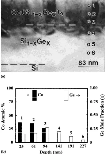
Co(Si1−xGex). An XTEM image of the sample annealed at 0.2 J/cm2is shown in Fig. 1(a), in which three distinct layers are present in the reacted region. From EDS/
XTEM analysis the Co concentration decreased along the film depth as shown in Fig. 1(b). To clearly show the concentration changes of Co and Ge for those of Si1−xGex and Si, respectively, in the Co(Si1−xGex), Co(Si1−xGex)2,
and Si1−xGexlayers, the Co and Ge concentration units in the figures, hereafter, are expressed as “atomic %” and “mole fraction (x)” respectively. From Fig. 1(b) it is evi-dent that on annealing at 0.2 J/cm2 the intermixing
be-tween Co and Si0.76Ge0.24 in the reacted region was not complete. Meanwhile some Ge segregated down to the bottom layer, indicating that Co tended to react pref-erably with Si. This result is presumably due to the higher heat of formation for Co–Si than for Co–Ge.21
From microdiffraction analysis the top layer was of amorphous structure and/or nanocrystal, whereas the middle and bottom layers were of Co(Si1−xGex) and Co(Si1−xGex)2 as shown in Fig. 1(c) and 1(d), respectively.
At 0.3 J/cm2Ge segregated out of the germanosilicide layers to the underlying Si0.76Ge0.24film, forming a
Ge-rich Si1−xGexlayer between the Co(Si1−xGex)2layer and
the residual Si0.76Ge0.24film. Meanwhile, the XRD
pat-terns in Fig. 2 show that after annealing at 0.3 J/cm2the
c-axis lattice constant of the residual Si0.76Ge0.24 film
was reduced compared with that of the as-grown Si0.76Ge0.24 film, revealing the occurrence of strain
re-laxation. Strain relaxation might be induced by the chemical inhomogeneities, e.g., Ge segregation, and de-fects present in the interface between the germanosilicide and the unreacted Si1−xGex film.
7,17,26–28
At 0.6 J/cm2 three germanosilicide layers were still present, and some Ge further diffused to the Si substrate, indicating that the melting depth exceeded the total thickness of the as-deposited Co layer (∼25 nm) and the as-grown Si0.76Ge0.24film (∼150 nm). Meanwhile the inhomoge-neous distribution of Co in the reacted region was sig-nificantly improved. At 0.8 J/cm2the reacted region was
mostly transformed to a single layer of Co(Si1−xGex)2, but more Ge diffused into the Si substrate as shown in Fig. 3. It is apparent that annealing at higher energy densities not only allowed the Co layer to react with more of the underlying Si0.76Ge0.24 film, facilitating the growth of Co(Si1−xGex)2, but also enhanced Ge diffusion down to the Si substrate. At energy densities >1.0 J/cm2, constitutional supercooling occurred, resulting in the cel-lular structures of Ge-deficient Si1−xGex islands sur-rounded by Co germanosilicide.
The above results have shown that one pulse annealing at an energy density of 0.2–1.0 J/cm2 can produce a three-layer germanosilicide film or a single-layer ger-manosilicide film with Ge diffusion down to the Si0.76Ge0.24 and Si substrates. Multiple pulse annealing
has been reported to effectively homogenize the Pd con-centration in the germanosilicide without inducing Ge segregation to the underlying Si0.76Ge0.24 film.
28
In the J-S. Luoet al.:Interfacial reactions of Co/Si0.76Ge0.24and Co(Si0.76Ge0.24)/Si0.76Ge0.24by pulsed KrF laser annealing
present study, therefore, multiple pulse annealing at 0.2 J/cm2was performed on some samples. The decision
to choose 0.2 J/cm2 as the energy density for multiple
pulse annealing is based on the result that on one pulse annealing at 0.2 J/cm2no Ge segregation out of the ger-manosilicide film occurred. For the sample annealed at 0.2 J/cm2for 5 pulses, two layers instead of three layers were formed in the reacted region. From electron diffrac-tion analysis the two layers were of Co(Si1−xGex) and Co(Si1−xGex)2, respectively. After annealing for 20
pulses the reacted region was mostly transformed to a smooth Co(Si1−xGex)2layer as shown in Fig. 4(a). It is
interesting to note that for a Co/Si0.76Ge0.24sample
an-nealed at 550 °C agglomeration occurred as shown in Fig. 5, in which Co(Si1−xGex) islands were surrounded by Ge-rich Si1−xGex. The EDS/XTEM data in Fig. 4(b) show that no Ge atoms segregated out of the germano-silicide to the underlying Si0.76Ge0.24film.
Correspond-ingly, the XRD patterns in Fig. 2 reveal that no apparent strain relaxation appeared in the residual Si0.76Ge0.24 film after annealing at 0.2 J/cm2 for 20 pulses. Similar
results were observed in the Pd/Si0.76Ge0.24 system.28
Those results imply that during the interfacial reactions of metal–Si1−xGex the strain relaxation of the residual Si1−xGexfilm can be suppressed by inhibiting Ge segre-gation out of the germanosilicide via pulsed KrF laser annealing. In the present study, we concluded that mul-tiple pulse annealing at 0.2 J/cm2is an effective method to produce a smooth Co(Si0.76Ge0.24)2 film without Ge
segregation out of the germanosilicide and inducing strain relaxation in the residual Si0.76Ge0.24film.
In addition, the repetition rate, 1 Hz, used in the pres-ent study was low enough to exclude the cumulative heating effect.32Therefore, these results also prove that phase transformation and the diffusion of chemical spe-cies can be proceeded by each individual laser pulse for FIG. 1. (a) XTEM image and (b) the depth profiles of Co and Ge for the Co/Si0.76Ge0.24sample annealed at 0.2 J/cm
2. Ge mole fraction (x) means
the mole fraction of Ge in Si1−xGexfor Co(Si1−xGex), Co(Si1−xGex)2, and Si0.76Ge0.24films, respectively. The areas probed by electron beam are
denoted as “O” and designated as 1, 2, 3, 4, and 5, respectively. (c) The [100] electron diffraction pattern (DP) of Co(Si1−xGex) and (d) the [110]
annealing at a low repetition rate. Similar results were found in the pulsed KrF laser annealing of Pd/ Si0.76Ge0.24.
28
B. Co(Si0.76Ge0.24)/Si0.76Ge0.24
It was reported23 that constitutional supercooling can
be suppressed by melting monosilicide or disilicide films; therefore, a simultaneous study of the Co(Si0.76Ge0.24)/Si0.76Ge0.24system by pulsed KrF laser annealing was also conducted. Figure 6 shows the XTEM image and EDS data of a Co(Si0.76Ge0.24) film grown at 250 °C. Although some Ge tended to segregate to the surface of the Co(Si0.76Ge0.24) film, both agglomeration and Ge segregation to the underlying Si0.76G0.24film did not appear. Therefore, the Co(Si0.76Ge0.24) films grown at 250 °C could be chosen as the precursors for subse-quent growth of the continuous Co(Si1−xGex)2films by
pulsed KrF laser annealing. On annealing at 0.2 J/cm2the Co(Si0.76Ge0.24) layer remained inert without
transform-ing to Co(Si1−xGex)2. At an energy density of 0.4–
0.8 J/cm2 a Co(Si1−xGex)2 layer was formed between
the Co(Si1−xGex) layer and the Si0.76Ge0.24 film. At
1.0 J/cm2a single-layer Co(Si1−xGex)2film was formed,
but some Ge diffused to the Si substrate. It is worth noting that an energy densities >1.6 J/cm2 even the monogermanosilicide, Co(Si0.76Ge0.24), could not
pre-vent the occurrence of constitutional supercooling.
In the present study the energy densities at which Co(Si1−xGex) transformation to Co(Si1−xGex)2, Ge
diffusion to the underlying Si, and constitutional super-cooling occurred were higher for the Co(Si0.76Ge0.24)/
Si0 . 7 6Ge0 . 2 4 system than for the Co/Si0 . 7 6Ge0 . 2 4 system. Similar results had been observed for Ni and Ni(Si0.76Ge0.24) on Si0.76Ge0.24.26,27 These phenomena
may be explained in terms of the strong coupling of ultraviolet radiation with metals.33
IV. SUMMARY AND CONCLUSIONS
(1) For the Co/Si0.76Ge0.24 samples annealed at an
energy density of 0.2–0.6 J/cm2 three germanosilicide layers, i.e., amorphous structure and/or nanocrystal, Co(Si1−xGex), and Co(Si1−xGex)2, were formed in
the reacted region along the film-depth direction. At 0.3 J/cm2, Ge started to segregate to the underlying FIG. 2. XRD patterns of the Co/Si0.76Ge0.24samples annealed at
vari-ous conditions.
FIG. 3. (a) XTEM image and (b) the depth profiles of Co and Ge for the Co/Si0.76Ge0.24sample annealed at 0.8 J/cm
2showing that a single
Co(Si1−xGex)2layer was formed concurrently with Ge diffusion to the
underlying Si substrate. Ge mole fraction (x) means the mole fraction of Ge in Si1−xGexfor Co(Si1−xGex)2and Si1−xGexfilms, respectively. The areas probed by electron beam are denoted as “O” and designated as 1, 2, 3, 4, 5, and 6, respectively.
Si0.76Ge0.24 film, inducing strain relaxation in the
residual Si0.76Ge0.24 film. At 0.8 J/cm 2
, the reacted region was mostly transformed to a single layer of Co(Si1−xGex)2, whereas Ge diffused to the Si substrate. At 1.0 J/cm2, constitutional supercooling appeared.
(2) For the Co/Si0.76Ge0.24sample multiple pulse an-nealing at 0.2 J/cm2is a novel method to form a smooth
Co(Si0.76Ge0.24)2 film without inducing Ge segregation out of the germanosilicide and apparent strain relaxation of the unreacted Si0.76Ge0.24film.
(3) When the monogermanosilicide, Co(Si0.76Ge0.24), was used as the starting material for laser annealing, the constitutional supercooling still occurred at energy den-sities >1.6 J/cm2.
(4) The energy densities at which Co(Si1−xGex) trans-formation to Co(Si1−xGex)2, Ge segregation to the
under-lying Si, and constitutional supercooling occurred were higher for the Co(Si0.76Ge0.24)/Si0.76Ge0.24 system than
for the Co/Si0.76Ge0.24system. FIG. 5. XTEM image for the Co/Si0.76Ge0.24 sample annealed at
550 °C showing that the Co(Si1−xGex) grains, A and B, are surrounded
by Ge-rich Si1−xGexfilm.
FIG. 6. (a) XTEM image and (b) the depth profiles of Co and Ge for the Co/Si0.76Ge0.24sample annealed at 250 °C. Ge mole fraction (x)
means the mole fraction of Ge in Si1−xGex for Co(Si1−xGex) and Si0.76Ge0.24films, respectively. The areas probed by electron beam are
denoted as “O” and designated as 1, 2, 3, and 4, respectively. FIG. 4. (a) XTEM image and (b) the depth profiles of Co and Ge for
the Co/Si0.76Ge0.24sample annealed at 0.2 J/cm
2for 20 pulses showing
that a smooth Co(Si1−xGex)2layer was formed without inducing Ge
segregation. Ge mole fraction (x) means the mole fraction of Ge in Si1−xGex for Co(Si1−xGex)2and Si0.76Ge0.24films, respectively. The
areas probed by electron beam are denoted as “O” and designated as 1, 2, 3, and 4, respectively.
ACKNOWLEDGMENT
This work was sponsored in part by the Republic of China National Science Council under Contract No. NSC-87-2216-E-006-023.
REFERENCES
1. F.Y. Huang, X. Zhu, M.O. Tanner, and K.L. Wang, Appl. Phys. Lett. 67, 566 (1995).
2. H. Presting, H. Kibbel, M. Jaros, R.M. Turton, U. Menczigar, G. Abstreiter, and H.G. Grimmeiss, Semicond. Sci. Technol. 1, 1127 (1992).
3. R.D. Thompson, K.N. Tu, J. Angillelo, S. Delage, and S.S. Iyer, J. Electrochem. Soc. 135, 3161 (1988).
4. Q.Z. Hong and J.W. Mayer, J. Appl. Phys. 66, 611 (1989). 5. H.K. Liou, X. Wu, U. Gennser, V.P. Kesan, S.S. Iyer, K.N. Tu,
and E.S. Yang, Appl. Phys. Lett. 60, 577 (1992).
6. A. Buxbaum, M. Eizenberg, A. Raizman, and F. Schaffler, Appl. Phys. Lett. 59, 665 (1991).
7. A. Buxbuam, E. Zolotoyabko, M. Eizenberg, and F. Schaffler, Thin Solid Films, 222, 157 (1992).
8. O. Thomas, S. Delage, F.M. d’Heurle, and G. Scilla, Appl. Phys. Lett. 54, 228 (1989).
9. W.J. Qi, B.Z. Li, W.N. Huang, Z.G. Gu, H.Q. Lu, X.J. Zhang, M. Zhang, G.S. Dong, D.C. Miller, and R.G. Aitken, J. Appl. Phys. 77, 1086 (1995).
10. D.B. Aldrich, Y.L. Chen, D.E. Sayers, R.J. Nemanich, S.P. Ash-burn, and M.C. Ozturk, J. Appl. Phys. 77, 5107 (1995). 11. D.B. Aldrich, H.L. Heck, Y.L. Chen, D.E. Sayers, and R.J.
Nemanich, J. Appl. Phys. 78, 4958 (1995).
12. A. Eyal, R. Brener, R. Beserman, M. Eizenberg, Z. Atzmon, D.J. Smith, and J.W. Mayer, Appl. Phys. Lett. 69, 64 (1996). 13. W. Freiman, A. Eyal, Y.L. Khait, R. Beserman, and K. Dettmer.
Appl. Phys. Lett. 69, 3821 (1996).
14. M.C. Ridgway, R.G. Elliman, N. Hauser, J.-M. Baribeau, and T.E. Jackman, in Advanced Metallization and Processing for
Semiconductor Devices and Circuits—II, edited by A. Katz,
S.P. Murarka, Y.I. Nissim, and J.M.E. Harper (Mater. Res. Soc. Symp. Proc. 260, Pittsburgh, PA 1992), p. 857.
15. F. Lin, G. Sarcona, M.K. Hatalis, A. F. Cserhati, E. Austin, and D.W. Greve, Thin Solid Films 250, 20 (1994).
16. Z. Wang, Y.L. Chen, H. Ying, R.J. Nemanich, and D.E. Sayers, in Silicides, Germanides, and Their Interfaces, edited by R.W. Fathauer, S. Mantl, L.J. Schowalter, and K.N. Tu. (Mater. Res. Soc. Symp. Proc. 320, Pittsburgh, PA, 1994), p. 397. 17. J.S. Juo, W.T. Lin, C.Y. Chang, W.C. Tsai, and S.J. Wang, Mater.
Chem. Phys. 48, 140 (1997).
18. V. Aubry, F. Meyer, R. Laval, C. Clerc, P. Warren, and D. Dutar-tre, in Silicides, Germanides, and Their Interfaces, edited by R.W. Fathauer, S. Mantl, L.J. Schowalter, and K.N. Tu. (Mater. Res. Soc. Symp. Proc. 320, 1994), p. 299.
19. Q.Z. Hong and J.W. Mayer, in Advanced Metallizations In
Micro-electronics, edited by A. Katz, S.P. Murarka, and A. Appelbaum.
(Mater. Res. Soc. Proc. 181, Pittsburgh, PA, 1990), p. 145. 20. E.J. Jaquez, A.E. Bair, and T.L. Alford, Appl. Phys. Lett. 70, 874
(1997).
21. Cohesion in Metals: Transition Metal Alloys, edited by F.R. De-boer, R. Boom, W.C. Mattens, A.R. Miedema, and A.K. Niessen, (North Holland, Amsterdam, 1988).
22. J.M. Poate, H.J. Leamy, T.T. Sheng, and G.K. Celler, Appl. Phys. Lett. 33, 918 (1978).
23. M. Witter and M. von Allmen, J. Appl. Phys. 50, 4786 (1979). 24. R.T. Tung, J.M. Gibson, D.C. Jacobson, and J.M. Poate, Appl.
Phys. Lett. 43, 476 (1983).
25. E. D’Anna, G. Leggieri, and A. Luches, Appl. Phys. A 45, 325 (1988).
26. J.S. Luo, W.T. Lin, C.Y. Chang, and W.C. Tsai, J. Appl. Phys. 82, 3621 (1997).
27. J.S. Luo, W.T. Lin, C.Y. Chang, and W.C. Tsai, Mater. Chem. Phys. 54, 160 (1998).
28. D.R. Chen, J.S. Luo, W.T. Lin, C.Y. Chang, and P.S. Shih, Appl. Phys. Lett. 73, 1355 (1998).
29. J.R. Abelson, T.W. Sigmon, K.B. Kim, and K.H. Weiner, Appl. Phys. Lett. 52, 230 (1988).
30. Z. Kantor, E. Fogarassy, A. Grob, J.J. Grob, D. Muller, B. Prevot, and R. Stuck, Appl. Phys. Lett. 69, 969 (1996).
31. J. Boulmer, P. Boucaud, C. Guedj, D. Debarre, D. Bouchier, E. Finkman, S. Prawer, K. Nugent, A. Desmur-Larre, C. Godet, and P.R. Cabarrocas, J. Crystal Growth 157, 436 (1995). 32. J. Brannon, Excimer Laser Ablation and Etching (American
Vacuum Society, New York, 1993).
33. E. D’Anna, G. Leggieri, and A. Luches, Appl. Phys. A 45, 325 (1988).