Abstract—Degradation of lateral diffused MOS transistors in
various hot-carrier stress modes is investigated. A novel
three-region charge-pumping technique is proposed to characterize
in-terface trap
(N
it) and bulk oxide charge Q
oxcreation in the
channel and in the drift regions separately. The growth rates
of
N
itand
Q
oxare extracted from the proposed method. A
two-dimensional numerical device simulation is performed to gain
insight into device degradation characteristics in different stress
conditions. This paper shows that a maximum
I
gstress causes the
largest drain current and subthreshold slope degradation because
of both
N
itgeneration in the channel and
Q
oxcreation in the
bird’s beak region. The impact of oxide trap property and location
on device electrical characteristics is analyzed from measurement
and simulation.
Index Terms—Hot-carrier degradation, lateral diffused MOS
(LDMOS), three-region charge pumping (CP).
I. I
NTRODUCTIONI
N RECENT years, multifunction power integrated chips
are strongly demanded for the market of portable devices,
automotive applications, and display drivers [1]. The integrated
bipolar, CMOS, and DMOS (BCD) process has been developed
to realize complex single power ICs [2], [3]. Among the
candi-dates of high-voltage devices, lateral diffused MOS (LDMOS)
transistors are attractive because they can be easily integrated
with standard low-voltage CMOS process [1]–[4]. The LDMOS
has been widely used in today’s high-voltage and high-current
output circuits [4], from a standard 12-V automotive battery [5]
to 100-V plasma display panel drivers [6].
One of the major reliability issues in an LDMOS is
hot-carrier injection and trapping in the oxide [7]. Various
hot-carrier stress modes have been reported. Different stress
conditions result in oxide damage of different types (
N
itand
Q
ox) and locations (channel or drift region). Moens et al.
reported that maximum
I
Bstress results in the worst
hot-carrier degradation for a gate oxide thickness from 7 nm [7]
Manuscript received April 21, 2006; revised July 19, 2006. This work was supported in part by Taiwan Semiconductor Manufacturing Company (TSMC) under TSMC-NCTU Joint Development Project and in part by the National Science Council, Taiwan, R.O.C., under Contract NSC94-2215-E009-009.
C.-C. Cheng, J. F. Lin, and T. Wang are with the Department of Electronics Engineering, National Chiao-Tung University, Hsinchu 300, Taiwan, R.O.C. (e-mail: twang@cc.nctu.edu.tw).
T. H. Hsieh, J. T. Tzeng, Y. C. Jong, R. S. Liou, S. C. Pan, and S. L. Hsu are with Taiwan Semiconductor Manufacturing Company, Hsinchu 300, Taiwan, R.O.C.
Digital Object Identifier 10.1109/TDMR.2006.883834
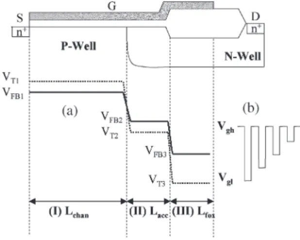
Fig. 1. (a) Cross section of an n-LDMOS and flatband (solid line) and threshold (dash line) voltage distributions. The device is divided into three parts, i.e., 1) Lchan (channel region), 2) Lacc (accumulation region), and
3)Lfox(field oxide region). (b) Illustration of a CP measurement waveform.
Vgh= 12 V is fixed, and Vglvaries from+3.6 to −40 V.
Fig. 2. Typical CP current in an n-LDMOS. The three stages of the CP current correspond to the three regions of the device. The flatband voltage of each region is indicated in the figure. The frequency in CP measurement is fixed at 200 kHz.
to 17 nm [8]. Their studies showed that gate oxide damage
occurs in the channel and in the accumulation regions. The
device characteristics degradation is attributed to interface trap
generation [7], [8]. Hefyene et al. [9] and Chen et al. [10]
claimed that maximum
I
gstress has more serious degradation,
and again, interface trap generation is the cause of degradation
[9], [10]. Since LDMOS degradation is closely dependent on
trap type and location, the profiling of trap spatial distribution
Fig. 3. Substrate current and gate current versus gate voltage in an LDMOS. Three different stress modes are shown in the figure, i.e., 1) mode A (maximumIb), 2) mode B(Vg∼ (1/2)Vd), and 3) mode C (maximum Ig).
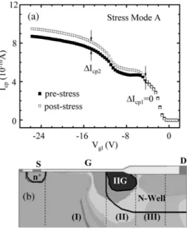
Fig. 4. (a) CP current versusVglbefore and after 1400-s mode A stress. (b) 2-D device simulation of IIG distribution in stress mode A.
and trap behavior is important to the understanding of the
impact of various hot-carrier stress modes.
In this paper, we demonstrate a novel three-region
charge-pumping (CP) technique to probe hot-carrier stress-induced
ox-ide damage in an LDMOS [11]. Each region of the CP current
corresponds to a different part of the device. By comparing
the prestress and poststress CP currents in each region, we are
able to identify the locations of oxide damage in the device
and corresponding trap properties. A two-dimensional (2-D)
device simulation is performed to identify an impact ionization
generation (IIG) region in the device. The dependence of device
degradation characteristic on trap position is also simulated.
II. T
HREE-R
EGIONCP M
EASUREMENTThe n-LDMOS used in this work was processed in a
0.18-
µm CMOS technology with a gate oxide thickness of
100 nm and a field oxide thickness of 500 nm. The operation
voltages are
V
g= 40 V and V
d= 40 V. Fig. 1(a) shows the
device cross section. The device is divided into three regions.
Fig. 5. (a) CP current versusVglbefore and after 1400-s mode B stress. The shift of the flatband voltage in stage 2 implies the generation of negative oxide charge in the accumulation region. (b) 2-D device simulation of IIG in stress mode B.
Fig. 6. CP results in stress mode B for different stress times.
Region (I) is the channel region. Regions (II) and (III) are the
accumulation region and the field oxide region, respectively.
The length of each region is denoted by
L
chan(= 3 µm), L
acc,
and
L
fox, respectively. The gate width is 20
µm, and the
threshold voltage is 1.5 V. The device flatband voltage (
V
FB,
solid line) and threshold voltage (
V
T, dash line) distributions of
the three regions are illustrated in Fig. 1(a). In the drift region,
the flatband voltage is higher than the threshold voltage because
of the n-type substrate.
The gate voltage waveform in CP measurement is illustrated
in Fig. 1(b) with a fixed
V
gh= 12 V and a variable V
gl. For
the 100-nm-thick gate oxide, we can switch
V
glfrom
+3.6
to
−40 V without a significant gate oxide tunneling current.
In this
V
glrange, all the three regions of the device can be
probed. The measurement frequency is 200 kHz. Typical CP
measurement result is shown in Fig. 2. The CP current
(I
cp)
exhibits three stages, which correspond to the three regions
of an n-LDMOS. It should be noticed that each stage has
its corresponding threshold and flatband voltages. By
mea-suring the change of
I
cpand
V
FBafter stress in each stage,
Fig. 7. Region (II) oxide-trapped charge growth rate in stress mode B.
Fig. 8. Linear drain current degradation(Idlin) rate measured at Vg/Vd=
40 V/0.1 V in stress mode B.
device [11], e.g.,
∆N
it(channel) = ∆I
cp(stage 1)/qfW L
chan,
∆Q
ox(acc) = ∆V
FB(stage 2) · C/q, and so on.
Three hot-carrier stress modes, i.e.: 1) mode A (maximum
I
b); 2) mode B
(V
g∼ (1/2)V
d); and 3) mode C (maximum I
g),
are investigated. The
I
g−V
gand
I
b−V
gof an n-LDMOS are
shown in Fig. 3. The maximum
I
b(mode A) stress is applied at
V
g/V
d= 8 V/50 V, whereas the maximum I
g(mode C) stress
is applied at
V
g/V
d= 50 V/50 V. The bias conditions of the
three stress modes are also indicated in Fig. 3. For each stress
mode, the three-region CP method is performed to investigate
trap type (
N
itor
Q
ox) and growth characteristics. Subthreshold
slope and linear drain current
(I
dlin) are measured to monitor
device degradation.
III. R
ESULTS ANDD
ISCUSSIONA. Maximum
I
bStress Mode
Fig. 4(a) shows the
I
cpin a fresh device and after 1400-s
maximum
I
bstress. The poststress
I
cpin the first stage is nearly
the same as the prestress one, indicating that region (I) oxide
is not damaged by the stress. The poststress
I
cpin stage 2,
however, exhibits an upward shift, while the flatband voltage
remains the same (no rightward shift in the
I
cp). This feature
suggests
N
itgeneration in region (II) but no
Q
oxcreation.
Numerical device simulation also shows the maximum IIG rate
in region (II) [Fig. 4(b)]. Although interface trap generation is
observed from the
I
cp, the subthreshold swing of the device
is not degraded because the generated
N
itis distributed in
region (II) rather than in the channel region. In addition,
I
dlindegradation is not observed either.
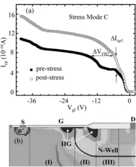
Fig. 9. (a) CP current before and after 1000-s mode C stress. Upward shift in first-stageIcpindicates interface trap generation in the channel, and rightward shift in second-stageIcpimplies oxide charge creation in the accumulation
region. (b) 2-D device simulation of IIG distribution in stress mode C. Two IIG regions are found: One is in the channel region, and the other is in the accumulation region.
Fig. 10. Subthreshold characteristics before and after mode C stress. The swing degradation is attributed to interface trap generation in the channel region.
Fig. 11. The linear drain current versusVgbefore and after mode C stress.
B.
V
g∼ (1/2) V
dStress Mode
The
I
cpresults before and after mode B stress (at
V
g/V
d=
30 V/50 V) are shown in Fig. 5(a).
N
itgeneration in stress
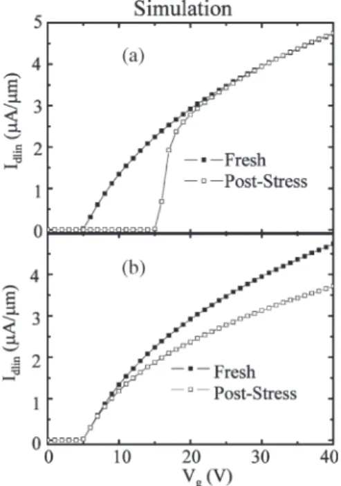
Fig. 12. Simulated drain current versus gate voltage without and with oxide charges. (a) Oxide charge is placed in the channel. (b) Oxide charge is placed in the bird’s beak region.
Fig. 13. Region (I) interface trap growth rate in stress mode C.
Fig. 14. Region (II) oxide charge growth rate in stress mode C.
substrate current [and a smaller IIG region in Fig. 5(b)], as
com-pared to stress mode A. Unlike stress mode A, a distinct
flat-band voltage shift in region (II) is noticed, which is manifested
by a rightward shift of the
I
cpin stage 2. An arrow is drawn
in Fig. 5(a) to indicate the flatband voltage shift
(∆V
FB2).
The rightward shift of the slope is caused by negative
Q
oxcreation in region (II). Fig. 6 shows the evolution of the
I
cpwith
Fig. 15. Idlindegradation versus stress time in stress mode C. The degrada-tion is mainly caused by negative oxide creadegrada-tion in the drift region.
TABLE I
SUMMARY OFMAJOROXIDE ANDDEVICEPERFORMANCE
DEGRADATIONS INVARIOUSSTRESSMODES
stress time. As stress time increases, the flatband voltage of the
region (II) continuously shifts to the right. The
Q
ox2generation
rate (Fig. 7) can be extracted from the
∆V
FB2versus stress
time by using the equation in Section II. Because of negative
Q
oxcreation, the resistance beneath the bird’s beak increases.
At a large
V
g, region (I) resistance is relatively small, and the
resistance in the bird’s beak region occupies a larger part of the
total resistance. Thus,
I
dlindegradation is observable at a higher
measurement
V
g= 40 V (Fig. 8). Numerical simulation for the
dependence of
I
dlindegradation on trap location will be given
later.
C. Maximum
I
gStress Mode
Fig. 9(a) shows the
I
cpresult before and after maximum
I
gstress for 1000 s. Two different stress-induced oxide
degra-dation mechanisms are noticed: One is
N
itgeneration in
region (I), and the other is negative
Q
oxcreation in region (II).
These two trap creation processes are reflected by an upward
shift of the first-stage
I
cpdenoted by
∆I
cp1and by a rightward
shift of the second-stage
I
cp[
∆V
FB2in Fig. 9(a)]. In contrast
to stress mode A, a 2-D device simulation reveals that the IIG
region in maximum
I
gstress splits into two parts [Fig. 9(b)]:
One is in the channel [region (I)], and the other is underneath
the bird’s beak. The
N
itgeneration in region (I) results in a
significant subthreshold swing degradation (Fig. 10) in stress
mode C. In addition,
Q
ox2creation accounts for a serious
I
dlindegradation (Fig. 11) in mode C. Fig. 11 shows that the
I
dlindegradation is more apparent at a larger
V
g. To explain the
V
gdependence, a 2-D device simulation is performed. We
calcu-late the
I
dlinversus
V
gby placing the same amount of fixed
oxide charge
(Q
ox/q = 10
19/cm
3) in the channel [Fig. 12(a)]
and in the bird’s beak region [Fig. 12(b)]. Fig. 12(a) shows a
larger
I
dlindegradation at a low
V
g, whereas Fig. 12(b) shows a
has the worst
I
dlindegradation. Due to oxide charge creation
in region (II), region (II) resistance increases, and the current
flow in region (II) is pushed deeper. Consequently, the electron
mobility exhibits a saturated effect, and thus,
I
dlindegradation
has a tendency to saturate in Fig. 15. This mobility saturation
model is also described in [13] and [14] for MOSFET and in
[8] for LDMOS structure. The LDMOS degradation behavior
and trap properties in the three stress modes are summarized
in Table I.
IV. C
ONCLUSIONA novel three-region CP technique has been developed to
characterize hot-carrier stress-induced oxide degradation in
each region of an n-LDMOS. The trap location and property
in various stress modes are identified, and their impact on
device characteristics has been analyzed. A correlation between
device degradation and CP and device simulation results has
been established. Our study reveals that the device subthreshold
swing degradation is mainly affected by interface traps in the
channel region, whereas the linear drain current degradation is
dictated by oxide-trapped charge in the drift region. Our study
also shows that maximum
I
gstress results in the worst
hot-carrier degradation in an LDMOS, which is attributed to both
N
itgeneration in the channel region and
Q
oxgeneration in the
bird’s beak region.
R
EFERENCES[1] E. M. Sankara Narayanan, G. A. J. Amaratunga, W. I. Milne, J. I. Humphret, and Q. Huang, “Analysis of CMOS-compatible lateral insulated base transistors,” IEEE Trans. Electron Devices, vol. 38, no. 7, pp. 1624–1632, Jul. 1991.
[2] B. J. Baliga, “An overview of Smart Power technology,” IEEE Trans.
Electron Devices, vol. 38, no. 7, pp. 1568–1575, Jul. 1991.
[3] C. Contiero, P. Galbiati, M. Palmieri, G. Ricotti, and R. Stella, “Smart Power approaches VLSI complexity,” in Proc. ISPSD, 1998, pp. 11–16. [4] P. L Hower and S. Pendharkar, “Short and long-term safe operating area
considerations in LDMOS transistors,” in Proc. IRPS, 2005, pp. 545–550. [5] J. G. Kassakian and D. J. Perreault, “The future of electronics in
automo-biles,” in Proc. ISPSD, 2001, pp. 15–19.
[6] J. Kim, T. M. Roh, S.-G. Kim, Q. S. Song, D. W. Lee, J.-G. Koo, K.-I. Cho, and D. S. Ma, “High-voltage power integrated circuit technology using SOI for driving plasma display panels,” IEEE Trans. Electron Devices, vol. 48, no. 6, pp. 1256–1263, Jun. 2001.
[7] P. Moens, G. Van den bosch, and G. Groeseneken, “Hot-carrier degrada-tion phenomena in lateral and vertical DMOS transistors,” IEEE Trans.
Electron Devices, vol. 51, no. 4, pp. 623–628, Apr. 2004.
[8] P. Moens, M. Tack, R. Degraeve, and G. Groeseneken, “A novel hot-hole injection degradation model for lateral nDMOS transistors,” in Proc.
IEDM, 2001, pp. 877–880.
[9] N. Hefyene, C. Anghel, R. Gillon, and A. M. Ionescu, “Hot carrier degradation of lateral DMOS transistor capacitance and reliability issues,” in Proc. IRPS, 2005, pp. 551–554.
drain n-channel metal–oxide–semiconductor field effect transistors,” Jpn.
J. Appl. Phys., vol. 33, no. 1B, pp. 606–611, Jan. 1994.
[14] R. Dreesen, K. Croes, J. Manca, W. De Ceuninck, L. De Schepper, A. Pergoot, and G. Groeseneken, “A new degradation model and lifetime extrapolation technique for lightly doped drain nMOSFETs under hot-carrier degradation,” Microelectron. Reliab., vol. 41, no. 3, pp. 437–443, Mar. 2001.
Chih-Chang Cheng (S’04) was born in Yi-Lan,
Taiwan, R.O.C., in 1980. He received the B.S. de-gree in physics from National Central University, Nanjing, Taiwan, R.O.C, in 2002. He is currently working toward the Ph.D. degree in electronics engineering from National Chiao-Tung University, Hsinchu, Taiwan, R.O.C.
His research interest includes high-voltage power device reliability and SPICE modeling.
J. F. Lin received the B.S. degree in electrophysics
from National Chiao-Tung University, Hsinchu, Taiwan, R.O.C., in 2005. He is currently working toward the M.S. degree at the same university.
His research interest includes high-voltage power devices and flicker noise.
Tahui Wang (S’84–M’85–SM’94) was born in
Taoyuan, Taiwan, R.O.C., on May 3, 1958. He re-ceived the B.S.E.E. degree from National Taiwan University, Taipei, Taiwan, R.O.C., in 1980 and the Ph.D. degree in electrical engineering from the Uni-versity of Illinois, Urbana-Champaign, in 1985.
From 1985 to 1987, he was with Hewlett-Packard Laboratories, Palo Alto, CA, where he was engaged in the development of GaAs HEMT devices and cir-cuits. Since 1987, he has been with the Department of Electronics Engineering, National Chiao-Tung University, Hsinchu, Taiwan, R.O.C., where he is currently a Professor. His research interests include hot-carrier phenomena characterization and reliability physics in VLSI devices, RF CMOS devices, and nonvolatile semiconductor devices.
Dr. Wang has served as a Technical Committee Member of many inter-national conferences, among them IEDM, IRPS, and VLSI-TSA. He was a recipient of the Best Teacher Award from Taiwan’s Ministry of Education.
T. H. Hsieh received the B.S. and M.S. degrees
in electrical engineering from National Tsing-Hua University, Taipei, Taiwan, R.O.C., in 1986 and 1988, respectively, and the Ph.D. degree in electrical engineering from National Chiao-Tung University, Hsinchu, Taiwan, R.O.C., in 1995.
From 1995 to 1999, he was with Vanguard In-ternational Development. In 2000, he joined Taiwan Semiconductor Manufacturing Company, Hsinchu, where he worked on SOI and 90-nm device process development. He is currently the Department Man-ager of the Product Device and SPICE Engineering Department, where he is responsible for the production yield and performance enhancement of device and SPICE engineering.
J. T. Tzeng received the B.S. and M.S. degrees in electrical engineering from
National Cheng-Kung University, Tainan, Taiwan, R.O.C., in 1995 and 1997, respectively.
He has been with Taiwan Semiconductor Manufacturing Company, Hsinchu, Taiwan, R.O.C, since 1999.
Y. C. Jong received the M.S. degree in physics from National Taiwan
Univer-sity, Taipei, Taiwan, R.O.C., in 1997.
He has been with Taiwan Semiconductor Manufacturing Company, Hsinchu, Taiwan, R.O.C., since 1999. His major focus includes nonvolatile memory process integration (1999–2003) and HV power CMOS process integration (2003–2005).
R. S. Liou received the B.S.E.E. degree from National Cheng-Kung University,
Tainan, Taiwan, R.O.C., in 1988.
He has been with Taiwan Semiconductor Manufacturing Company, Hsinchu, Taiwan, R.O.C., since 1990. His major focus includes Si/SiGe BiCMOS process integration (2000–2002) and HV power CMOS process integration (2002–2005).
Samuel C. Pan (S’83–M’87) received the B.S.
de-gree in electrical engineering from National Taiwan University, Taipei, Taiwan, R.O.C., in 1980 and the M.S. and Ph.D. degrees in electrical engineering from the University of Illinois, Urbana-Champaign, in 1984 and 1986, respectively.
From 1983 to 1986, he was a Research Assistant with the Solid State Electronics Laboratory, Uni-versity of Illinois, Urbana-Champaign. In 1987, he joined Intel Corporation as a Senior Device Physicist and worked on 0.8-µm Flash EPROM development and 0.6-µm CMOS process development. In 1995, he became Staff Circuit Designer and worked on 0.25-µm Pentium/Pro microprocessor with the focus on cache memory and PLA design. At the end of 1996, he moved back to Taiwan and joined Macronix International Co., Ltd., as Quality and Reliability Deputy Director. In 1999, he was named Technical Director to lead process development for 0.18- to 0.15-µm Flash and mask ROM memory technologies. In June 2003, he joined Taiwan Semiconductor Manufacturing Company, Hsinchu, Taiwan, R.O.C., as the Director of Advanced Product Engineering. His current interests include device physics, device/Flash cell reliability, failure analysis techniques, and methodologies for technology development and yield enhancement.
Dr. Pan is a member of Phi Kappa Phi and Eta Kappa Nu.
S. L. Hsu received the M.S. degree in material
science and engineering from National Cheng Kung University, Taiwan, R.O.C., in 1984 and the Ph.D. degree in electrical engineering from National Chiao Tung University, Taiwan, in 1994.
In the last three years, he was Fab-1 and Fab-2 Director of Taiwan Semiconductor Manufacturing Company (TSMC) and led Flip-Chip Division. He is currently Director of Fab-2 and High-Voltage Pro-gram at TSMC, Hsinchu, Taiwan.