954 IEEE ELECTRON DEVICE LETTERS, VOL. 30, NO. 9, SEPTEMBER 2009
MILC-TFT With High-
κ
Dielectrics for
One-Time-Programmable Memory Application
Tsung-Yu Chiang, Ming-Wen Ma, Yi-Hong Wu, Po-Yi Kuo, Kuan-Ti Wang,
Chia-Chun Liao, Chi-Ruei Yeh, and Tien-Sheng Chao
Abstract—In this letter, for the first time, one-time-programmable (OTP) memory fabricated on the low-temperature poly-Si p-channel thin-film transistor (TFT) with metal-induced lateral-crystallization channel layer and high-κ dielectrics is demonstrated. The state of this OTP memory can be identified by the scheme of gate-induced drain leakage current measurement. The OTP-TFT memory has good electrical characteristics in terms of low threshold voltage Vth∼ −0.78 V, excellent subthreshold swing∼105 mV/dec, low operation voltage, faster programming speeds, and excellent reliability characteristics.
Index Terms—Gate-induced drain leakage (GIDL), metal-induced lateral crystallization (MILC), one-time programmable (OTP), thin-film transistor (TFT).
I. INTRODUCTION
R
ECENTLY, nonvolatile memories have become very pop-ular for the applications of portable electronics, in which high density of nonvolatile memory is inevitable. The scaling down of traditional memories has met physical limits due to the aggressive scaling down of the photolithography and tunneling oxide thickness [1], [2]. However, low-temperature poly-Si thin-film transistors (LTPS-TFT) have been widely used for the application of system on panel (SOP) [3] and 3-D circuit-integration elements such as SRAMs, DRAMs, and nonvolatile memories [4]–[6]. Ultrahigh density memories have also been completed using 3-D multilayer stack LTPS-TFT memories. Unfortunately, it is difficult to fabricate nonvolatile memories without any extra mask and processing. Furthermore, many defects occur among the polysilicon channel films because of the large number of grain boundaries, resulting in much poor subthreshold swing (SS) and high threshold voltage (Vth) [7], [8]. In this letter, for the first time, the LTPS p-channel TFT with metal-induced lateral-crystallization (MILC) channel layer for the dual application of high-performance device and excellent reliable one-time-programmable (OTP) memory is successfullyManuscript received June 15, 2009. First published August 4, 2009; current version published August 27, 2009. This work was supported by the National Science Council, Taiwan, under Contract NSC-97-2221-E-009-153-MY3. The review of this letter was arranged by Editor J. K. O. Sin.
T.-Y. Chiang, Y.-H. Wu, P.-Y. Kuo, K.-T. Wang, C.-C. Liao, C.-R. Yeh, and T.-S. Chao are with the Department of Electrophysics, National Chiao Tung University, Hsinchu 300, Taiwan (e-mail: [email protected]; [email protected]; [email protected]; dennis5168@gmail. com; [email protected]; [email protected]; [email protected]. edu.tw).
M.-W. Ma is with the Institute of Electronics, National Chiao Tung Univer-sity, Hsinchu 300, Taiwan (e-mail: [email protected]).
Color versions of one or more of the figures in this letter are available online at http://ieeexplore.ieee.org.
Digital Object Identifier 10.1109/LED.2009.2027035
Fig. 1. Cross-sectional scheme of the OTP-TFT memory with MILC poly-crystalline silicon channel film and illustration of electron trapping for program state.
proposed. The performance of the LTPS-TFT device, which is demonstrated using the MILC method and HfO2 gate dielec-tric, is improved. Moreover, the OTP-TFT memory has been fabricated without any extra mask and processing. This process is simple and fully compatible with standard LTPS-TFT. The MILC-TFT with HfO2 gate dielectric can be used as OTP memories by measuring the change of gate-induced drain leak-age (GIDL) current [9], [10]. The OTP-TFT memory with lower Vth, excellent SS, lower operation voltage, longer reten-tion time, and good read disturbance can be obtained, highly promising for the realization of SOP and 3-D circuit integration.
II. EXPERIMENTALPROCEDURE
The device cross section of the OTP-TFT memory with HfO2dielectric and MILC polycrystalline silicon channel film is shown in Fig. 1. First, 500-nm thermal oxide was grown on the Si wafer by furnace system. Undoped amorphous Si (α-Si) layer with a thickness of 50-nm was deposited by low-pressure chemical vapor deposition at 550 ◦C. A 5-nm Ni layer was deposited by an electron-beam evaporation system at room tem-perature and patterned by liftoff process as a seed layer to crys-tallize the α-Si. Then, the 50-nm α-Si layer was cryscrys-tallized by the MILC process at 550◦C for 24 h in a N2ambient. To reduce Ni contamination, the residual Ni was removed by H2SO4+ H2O2. The source and drain (S/D) regions in the device active region were implanted with boron (10 keV at 5× 1015 cm−2) and activated at 600 ◦C for 24 h annealing in a N2 ambient. A 500-nm plasma-enhanced chemical-vapor-deposition oxide was deposited at 300 ◦C for device isolation. The device active region was formed by patterning and etching isolation oxide. Next, a 50-nm HfO2with effective oxide thickness EOT
CHIANG et al.: MILC-TFT WITH HIGH-κ DIELECTRICS 955
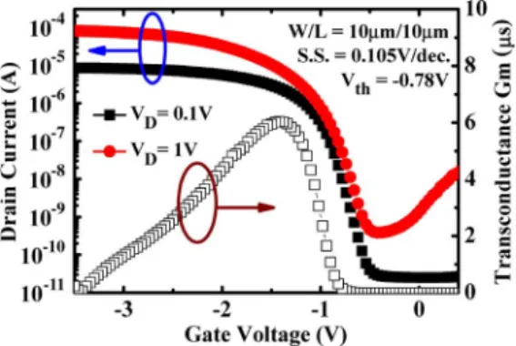
Fig. 2. Room temperature transfer characteristics (ID–VGand
transconduc-tance Gm) of the OTP-TFT memory with MILC polycrystalline silicon channel film (VD=|VDS|).
Fig. 3. Program speed characteristics of the OTP-TFT memory with MILC polycrystalline silicon channel film at different operating voltages.
∼12.3 nm was deposited by electron-beam evaporation system
at room temperature. Then, after the patterning of S/D contact holes, a 500-nm Al was deposited by electron-beam system evaporation at room temperature and patterned as Al gate and S/D contact pads. There was no other treatment during fabrication. The standard MILC LTPS-TFT and OTP memory can be fabricated simultaneously. This process is simple and fully compatible with standard LTPS-TFT.
III. RESULTS ANDDISCUSSION
Fig. 2 shows the transfer characteristics (ID–VG and Gm)
of the OTP-TFT memory with MILC polycrystalline silicon channel film. The device with gate length (L) and width (W ) of 10 and 10 μm, respectively, was measured. The thresh-old voltage (Vth) of the device was defined as the VG at
which the normalized drain-current reaches W/L × 10 nA for VD=−0.1 V. The OTP device has superior performance,
with smaller Vth (∼−0.78 V), excellent subthreshold swing (∼105 mV/dec) and higher drain current. A high gate-capacitance density, which corresponds to low EOT∼12.3-nm, is obtained from the capacitance–voltage curve of Al/HfO2on a P-type substrate to extract the gate-capacitance density of OTP-TFT memory (not shown).
In addition, this high-performance MILC-TFT device can also be used as an OTP memory device at sufficient gate voltage and drain voltage operation. The program speed character-istics of OTP-TFT devices with different operating voltages are shown in Fig. 3. The OTP-TFT device is programmed
Fig. 4. Data retention characteristics of OTP-TFT memory for the different bake temperatures. After 10k s at 25◦C, no significant GIDL current shift occurred.
Fig. 5. Read disturbance characteristics obtained for the OTP-TFT memory (stress voltage on VG= 2 V and VD=−1 V).
using electron gate injection mechanism for OTP memory application. The program conditions are follows: VG=−1 V
and VD= 9, 10, 11, and 12 V. The change of GIDL current
(IGIDL) may be read from Fig. 3. The IGIDL was measured from the OTP-TFT device with VG = 2 V and VD=−1 V.
The higher current (1 μA) and lower current (500 pA) of IGIDL were defined as the erased state (“0” state) and programmed state (“1” state), respectively. The memory states of MILC-TFT memory can be determined from the GIDL current under forward read operation [9], [10]. In the trapping location, the electrons have been trapped in the HfO2layer at the gate and drain overlap region (in Fig. 1). Furthermore, the GIDL current is reduced owing to the electron trapping at the gate and drain overlap region. The lower GIDL current can be attributed to the decrease of vertical electric field. A higher voltage for VD
trends to result in larger IGIDLchange and faster programming speed owing to the higher local electric field near the drain side. Comparing OTP-TFT memory with other LTPS-TFT memory devices, the programming voltage and read voltage are rela-tively smaller [12].
Fig. 4 shows the data retention performance which is mea-sured at room temperature and 85 ◦C. At room tempera-ture, charge loss can be barely observed up to 104 s. The OTP-TFT device with HfO2gate dielectric exhibits good reten-tion characteristics at room temperature and high temperature due to the deep-trapping level in the HfO2 layer. The results indicate that the IGIDL change is still retained about three orders after 104 s at 85 ◦C. Hence, the trapped electrons in the OTP-TFT memory with the HfO2 dielectric are not easily
956 IEEE ELECTRON DEVICE LETTERS, VOL. 30, NO. 9, SEPTEMBER 2009
detrapped. In addition, the measured read-disturb characteris-tic is shown in Fig. 5. The stress voltage was set at VG =
2 V and VD=−1 V. The IGIDL is slightly increased after 103 s, due to the electron detrapping by the stress voltage. Consequently, the IGIDLchange is maintained about three or-ders after 103s read disturb. Compare with other TFT-memory devices [12]–[14], OTP-TFT devices can be operated at lower voltages and higher program/erasing speeds with better charge retention over the same period of time.
IV. CONCLUSION
For the first time, a high-performance LTPS p-channel TFT with MILC channel layer with HfO2 gate dielectric used for OTP memory is successfully fabricated. This novel structure has excellent characteristics: low threshold voltage, excellent subthreshold swing, low operation voltage, faster program-ming speeds, and excellent reliability characteristics. OTP-TFT memory offers a very promising solution for the application of SOP and 3-D circuit integration.
ACKNOWLEDGMENT
The authors would like to thank the processes support from the National Nano Device Laboratories and the Nano Facility Center of the National Chiao Tung University.
REFERENCES
[1] K. Prall, “Scaling non-volatile memory below 30 nm,” in Proc. NVSMW Tech. Dig., 2007, pp. 5–10.
[2] T. Y. Chiang, T. S. Chao, Y. H. Wu, and W. L. Yang, “High-program/erase-speed SONOS with in situ silicon nanocrystals,” IEEE Electron Device Lett., vol. 29, no. 10, pp. 1148–1151, Oct. 2008.
[3] K. Yoneda, R. Yokoyama, and T. Yamada, “Development trends of LTPS TFT LCDs for mobile applications,” in VLSI Symp. Tech. Dig., 2001, pp. 85–90.
[4] F. Hayashi, H. Ohkubo, T. Takahashi, S. Horiba, K. Node, T. Uchida, T. Shimizu, N. Sugawara, and S. Kumashiro, “A highly stable SRAM memory cell with top-gate P-N drain poly-Si TFT of 1.5 V operation,” in IEDM Tech. Dig., 1996, pp. 283–286.
[5] H. J. Cho, F. Nemati, P. B. Griffin, and J. D. Plummer, “A novel pillar DRAM cell for 4 Gbit and beyond,” in VLSI Symp. Tech. Dig., 1998, pp. 38–39.
[6] Y. H. Lin, C. H. Chien, T. H. Chou, T. S. Chao, and T. F. Lei, “Impact of channel dangling bonds on reliability characteristics of Flash memory on poly-Si thin films,” IEEE Electron Device Lett., vol. 28, no. 4, pp. 267–269, Apr. 2007.
[7] M. W. Ma, C. Y. Chen, C. J. Su, W. C. Wu, Y. H. Wu, T. Y. Yang, K. H. Kao, T. S. Chao, and T. F. Lei, “Impacts of fluorine ion im-plantation with low-temperature solid-phase crystallized activation on high-κ LTPS-TFT,” IEEE Electron Device Lett., vol. 29, no. 2, pp. 168– 170, Feb. 2008.
[8] R. E. Proano, R. S. Misage, and D. G. Ast, “Development and elec-trical properties of undoped polycrystalline silicon thin-film transistor,” IEEE Trans. Electron Devices, vol. 36, no. 9, pp. 1915–1922, Sep. 1989.
[9] A. Padilla, K. Shin, T. J. King Liu, J. W. Hyun, I. Yoo, and Y. Park, “Dual-bit gate-sidewall storage FinFET NVM and new method of charge detection,” IEEE Electron Device Lett., vol. 28, no. 6, pp. 502–505, Jun. 2007.
[10] A. Padilla, S. Lee, D. Carlton, and T. J. King Liu, “Enhanced endurance of dual-bit SONOS NVM cells using the GIDL read method,” in VLSI Symp. Tech. Dig., 2008, pp. 142–143.
[11] C. C. Yeh, T. Wang, Y. Y. Liao, W. J. Tsai, T. C. Lu, M. S. Chen, Y. R. Chen, K. F. Chen, Z. T. Han, M. S. Wong, S. M. Hsu, N. K. Zous, T. F. Ou, W. C. Ting, J. Ku, and C. Y. Lu, “A novel NAND-type PJINES nitride trapping storage Flash memory cell with physically 2-bits-per-cell storage, and high programming throughput for mass storage applications,” in VLSI Symp. Tech. Dig., 2005, pp. 116–117.
[12] Y. H. Lin, C. H. Chien, T. H. Chou, T. S. Chao, and T. F. Lei, “Low-temperature polycrystalline silicon thin-film Flash memory with hafnium silicate,” IEEE Trans. Electron Devices, vol. 54, no. 3, pp. 531–536, Mar. 2007.
[13] Z. Pei, A. Chung, and L. Hwang, “Nonvolatile polycrystalline silicon thin film transistor memory using silicon-rich silicon nitride as charge storage layer,” Appl. Phys. Lett., vol. 90, no. 22, p. 223 515, Jun. 2007.
[14] S. C. Chen, T. C. Chang, P. T. Liu, Y. C. Wu, P. S. Liu, B. H. Tseng, J. H. Shy, S. M. Sze, C. Y. Chang, and C. H. Lien, “A novel nanowire channel poly-Si TFT functioning as transistor and nonvolatile SONOS memory,” IEEE Electron Device Lett., vol. 28, no. 9, pp. 809–811, Sep. 2007.