IEEE ELECTRON DEVICE LETTERS, VOL. 21, NO. 3, MARCH 2000 123
A New Observation of Band-to-Band Tunneling
Induced Hot-Carrier Stress Using Charge-Pumping
Technique
Yu-Lin Chu, Student Member, IEEE, and Ching-Yuan Wu, Member, IEEE
Abstract—The lateral distributions of interface-states ( it) and oxide-trapped charges ( ox) generated by band-to-band tunneling (BTBT) induced hot-carrier stress are analyzed by the new charge-pumping method. It is shown that the interface-states and oxide-trapped charges should be originated from different types of carriers due to the separation of the locations of their peak values. The further evidence of the measured distribution of the interface-states in the band-gap shows that the carriers travelled toward the gate edge would be the dominant carrier for the generation of interface-states while the carriers travelled away from the gate edge will generate oxide-trapped charges through the help of the vertical electric field. These results should be very useful for the reliability analysis of flash memories.
Index Terms—BTBT, Charge-pumping technique, inter-face-states, MOSFET, oxide-trapped charges.
I. INTRODUCTION
B
AND-TO-BAND tunneling induced hot-carrier stress is one of the most serious reliability issues for deep-sub-micrometer MOSFET's and flash memories. With the contin-uing scaling down of MOS devices, the electric field under the gate-to-drain overlap region would be very large when the de-vice is operated in off-state, and the significant BTBT current may exist and interface-states and oxide-trapped charges might be generated. For flash memories, among many erase methods, the gate edge Fowler–Nordheim (F–N) tunneling mechanism has been widely used to discharge the floating gate electrode; the source-side erase generates electrons and holes through the surface-field induced band-to-band tunneling in the N -to-gate overlap region, and some of these holes may gain enough energy from the lateral electric field and can inject into the oxide with the help of a negative gate bias [1], [2]. Some researchers [3], [4] thought that the carriers traveling away from the gate edge would be the dominant effect for the generation of interface-states and oxide-trapped charges, and the damages caused by the carriers traveling toward the gate edge were not be considered. More recently, the electron injection method using band-to-band tunneling induced electrons (BBHE) for flash memory with a p-channel cell was proposed [5], which ensures the realizationManuscript received August 2, 1999; revised November 8, 1999. This work was supported by the National Science Council, Taiwan, R.O.C., under Contract NSC–89-2215-E009-070. The review of this paper was arranged by Editor D. J. Dumin.
The authors are with the Advanced Semiconductor Device Research Labora-tory and Institute of Electronics, National Chiao-Tung University, Hsinchu 300, Taiwan, R.O.C. (e-mail: [email protected]).
Publisher Item Identifier S 0741-3106(00)02107-8.
of high program efficiency, high scalability and hot-hole-in-jection-free operation. Therefore, the realibility issues of the BBHE deserves further study. In this letter, the new charge-pumping technique was used to profile the interface-state dis-tributions in the band-gap and the lateral distribution of inter-face-states and oxide-trapped charges, which can help us realize what kind of carriers may be the dominant effect for the gener-ation of the interface-states or oxide-trapped charges.
II. EXPERIMENTALTECHNIQUE
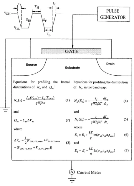
The recently developed new charge-pumping technique [6] was used to profile the lateral distribution of and . Fig. 1 shows the experimental setup for charge-pumping current measurement, where the gate pulse is provided by a HP8110 pulse generator and a HP4145B parameter analyzer is used to monitor the charge-pumping current. Keeping the rising slope and falling slope constant and varying the high-level and base-level of the gate pulse, the lateral distri-butions of and can be obtained. The equations used to calculate and are given in the insert of Fig. 1, where
is channel width; is the frequency of the gate pulses; is the effective charge-pumping region defined by and
is the half-maximum value of curve before (after) stress while
is that of curve before (after) stress. In our new charge-pumping technique, relataed to
is extracted from the saturation value of
curve. In addition, is extracted
from curves before (after) stress so that the interference induced by the generated for extracting can be eliminated by our method. Hence, a reliable lateral distribution of can be obtained.
To profile the distribution of in the band-gap, and , which are the rise time and fall time , are varied with fixed and to detect the lower part and upper part of in the band-gap, respectively. According to [7], the distribu-tion in the upper part and lower part of the bandgap can be ex-tracted by the equations listed in the insert of Fig. 1, where is the intrinsic Fermi energy; is the electron (hole) cap-ture-cross-section; is the thermal velocity; is the intrinsic carrier concentration, and is the nonsteady-state electron (hole) emission time. Note that are extracted from (21) and (22) using our previous work [8].
The test device is a conventional counter-implanted p-MOSFET with the mask length of 0.85 m, the channel width of 120 m and the oxide thickness of 110 Å, the
124 IEEE ELECTRON DEVICE LETTERS, VOL. 21, NO. 3, MARCH 2000
Fig. 1. Experimental setup of the charge-pumping measurement and the shape of the gate pulse. The inserts are the equations used to extractN and Q .
device structure parameters used in two-dimensional (2-D) device simulation are extracted by accurately simulating the current–voltage (I–V) characteristics of the fresh devices.
In our experiment, the measured data of the BTBT current is simulated by a new quasi–2-D BTBT current model [9] first, then the stress condition of V and V is chosen for the BTBT-induced hot-carrier stress to ensure that the damages are mainly generated by the carriers induced by the BTBT. The simulated result also reveals that the BTBT mainly occurs at the point where the drain concentration is
cm .
III. RESULTS ANDDISCUSSION
Based on our developed new charge-pumping technique, the interface-states and the oxide-trapped charges generated by BTBT-induced hot carrier stress were measured.
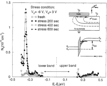
Fig. 2 shows that significant interface-states and electron-traps are generated with cumulative stress time. It should be noted that their positions of the peak value do not locate at the same point. This is different to the result shown in [4], where
they thought that the interface-states and oxide-trapped charges were generated by the carriers traveling away from the gate edge so that the locations of the peak value of both the inter-face-states and oxide-trapped charges should be the same and were ahead of the peak electric field. In theory, excluding the measurement errors, the locations of the peak interface-states and oxide-trapped charges should coincide each other if the in-terface-states and oxide-trapped charges are generated by the same carriers. But, according to our measured distribution of the interface-states in the band-gap shown in Fig. 3, the in-terface-states are mainly generated near the valance-band edge with cumulative stress time. Because the electrons may travel only in the conduction-band while the holes may travel only in the valance-band. Therefore, the hot electrons may have the higher probability to generate interface-states near the conduc-tion-band edge while the hot holes may have the higher prob-ability to generate those near the valance-band edge. This im-plies that the dominant carrier for the generation of the inter-face-states is hole, that is, the carriers traveling toward the gate edge. Therefore, according to Figs. 2 and 3, the mechanism
CHU AND WU: BAND-TO-BAND TUNNELING INDUCED HOT-CARRIER STRESS 125
Fig. 2. Lateral distribution of the cumulative interface-states and oxide-trapped charges with the stress condition of V = 06 V and
V = 3 V.
Fig. 3. Distribution of the cumulative interface-states in the band-gap with the stress condition ofV = 06 V and V = 3 V for conventional counter-implanted p-MOSFET. The inserts are the band structure reflecting the BTBT process and the physical direction of travel for the various carriers involved.
that the generated interface-states and oxide-trapped charges by the BTBT induced hot-carrier stress can be explained as fol-lows. Taking p-MOSFET for example, as mentioned in Sec-tion II, the simulated results of BTBT current show that the BTBT mainly occurs at the point where the drain concentra-tion is cm , which just locate between the peak value of the profiled interface-states and oxide-trapped charges shown in Fig. 2, as we inspect the simulated drain profile. Thus, as shown in the insert of Fig. 3, when the electron tunneling from the valance-band to the conduction-band, the electron will travel toward the channel region and may inject into the gate oxide with the help of the vertical electric field and would re-sult in the generated oxide-trapped charges, as noted by many studies [1]–[4], while the generated holes in the valance-band
Fig. 4. Distribution of the cumulative interface-states in the band-gap with the stress condition ofV = 8 V and V = 06 V for LDD n-MOSFET.
will travel away from the channel region and would be acceler-ated by an increasing lateral electric field; eventually, the holes will become hot enough and then relax their energy to generate the interface-states.
To further verify our viewpoint, the distribution of inter-face-states in the band-gap for LDD n-MOSFET with the mask length of 0.8 m, the channel width of 120 m and the oxide thickness of 110 Å was measured. As shown in Fig. 4, the interface-states are generated almost near the condution band edge, while those near the valance-band edge are nearly invariant with increasing the stress time. Therefore, the same as p-MOSFET, the generated interface-states are mainly con-tributed by the carriers traveling toward the gate edge, namely, electrons for LDD n-MOSFET.
IV. CONCLUSION
The separation of the peak value of the lateral dirstributions of interface-states and oxide-trapped charges generated by the BTBT induced hot-carrier stress reveals that the interface-states and oxide-trapped charges might be originated from different types of carriers. The distribution of interface-states in the band-gap shows that the carriers traveling toward the gate edge may encounter an increasing electric field and become hot to generate the interface-states, while the carriers traveling away from the gate edge may encounter a decreasing lateral electric field and might not be hot enough to generate the interface-states, but have the probability to inject into the gate oxide and generate oxide-trapped charges through the polarity of applied gate bias.
REFERENCES
[1] S. Hadded et al., “An investigation of erase-mode dependent hole trap-ping in flash EEPROM memory cell,” IEEE Electron Device Lett., vol. 11, pp. 514–516, Nov. 1990.
[2] T. C. Ong et al., “Erratic erase in ETOX flash memory array,” in Proc. IEEE VLSI Technology. Symp., 1993, pp. 83–84.
[3] J. Chen et al., “Short channel enhanced degradation during discharge of flash EEPROM memory cell,” in IEDM Tech. Dig., 1995, pp. 331–334.
126 IEEE ELECTRON DEVICE LETTERS, VOL. 21, NO. 3, MARCH 2000
[4] C. Chen and T. P. Ma, “Direct lateral profiling of hot-carrier-induced oxide charge and interface traps in thin gate MOSFET's,” IEEE Trans. Electron Devices, vol. 45, pp. 512–520, Feb. 1998.
[5] T. Ohnakado et al., “Novel electron injection method using band-to-band tunneling induced hot electron (BBHE) for flash memory with a
p-channel cell,” in IEDM Tech. Dig., 1995, pp. 279–282.
[6] Y. L. Chu, D. W. Lin, and C. Y. Wu, “A new charge-pumping tech-nique for profiling the interface-states and oxide-trapped charges,” IEEE Trans. Electron Devices, vol. 46, Feb. 2000.
[7] G. Groeseneken, H. Maes, N. Beltran, and R. DeKeersmaecker, “A re-liable approach to charge-pumping measurements in MOS transistors,” IEEE Trans. Electron Device, vol. ED-31, pp. 42–53, Jan. 1984. [8] H. H. Li, Y. L. Chu, and C. Y. Wu, “A new simplified charge-pumping
current model and its model parameter extraction,” IEEE Trans. Electron Devices, vol. 43, pp. 1857–1863, Nov. 1996.
[9] K. F. You and C. Y. Wu, “A new quasi-2D model for hot-carrier band-to-band tunneling current,” IEEE Trans. Electron Devices, vol. 46, pp. 1174–1179, June 1999.