國
立
交
通
大
學
電機學院微電子奈米科技產業研發碩士班
碩
士
論
文
利用陽極電極的調變來改善氧化鉿薄膜之電阻
式轉換記憶體其單極操作特性研究
Modification on unipolar resistive switching
characteristics of HfO
Xmemory film by top electrode
metal
研 究 生:賴威仁
指導教授:張國明 教授
利用陽極電極的調變來改善氧化鉿薄膜之電阻
式轉換記憶體其單極操作特性研究
Modification on unipolar resistive switching
characteristics of HfO
Xmemory film by top electrode
metal
研 究 生:賴威仁 Student:Wei-Ren Lai
指導教授:張國明 博士 Advisor:Dr. Kow-Ming Chang
國 立 交 通 大 學
電機學院微電子奈米科技產業研發碩士班
碩 士 論 文
A Thesis
Submitted to College of Electrical and Computer Engineering National Chiao Tung University
in partial Fulfillment of the Requirements for the Degree of Master
in
Industrial Technology R & D Master Program on Microelectronics and Nano Sciences
September 2009
Hsinchu, Taiwan, Republic of China
利用陽極電極的調變來改善氧化鉿薄膜之電阻
式轉換記憶體其單極操作特性研究
學生:賴威仁
指導教授:張國明 博士
國立交通大學電機學院產業研發碩士班
摘
要
這篇論文中,首先我們探討不同限流對電阻式記憶體的影響,然
後利用不同的金屬當上電極於氧化鉿/氮化鈦的結構,接著討論電極
與各種金屬的功函數和各種金屬的氧化自由能之間的關係。在同樣限
流下,可觀察到氧化自由能較低的金屬,沒有電阻式操作的特性,而
且氧化自由能較高的金屬,耐操度較差。因為自由能較低的金屬容易
在接面處形成金屬氧化物,會導致細絲無法燒斷且不能電阻式操作,
而自由能較高的金屬容易在電阻式操作中失去氧離子。因此我們研究
用惰性金屬/易反應金屬來當上電極,例如鈀/鋁、鈀/鈦、鉑/鈦等。此
種結構具有非常好的電阻式操作的特性,可在高溫下操作,耐久性測
試中可轉態超過 4000 次,資料保存能力可達十年。我們的研究顯示
惰性金屬/易反應金屬/氧化鉿/氮化鈦的電阻式記憶體是很有希望被
應用在下個世代的非揮發性記憶體。
Modification on unipolar resistive switching
characteristics of HfO
Xmemory film by top electrode
metal
Student:Wei-Ren Lai
Advisors:Dr. Kow-Ming Chang
Industrial Technology R & D Master Program of
Electrical and Computer Engineering College
National Chiao Tung University
ABSTRACT
In this thesis, first, we discuss to influence resistive memory for different compliance current, then the different metals were used as the electrode based on the HfOX/TiN
structure. Afterward, we discuss the electrode dependence with various metals work function and free energy of oxidation of various metals. For the same compliance current, lower free energy of oxidation of metals were observed no resistive switching characteristics, and higher free energy of oxidation of metals is bad for endurance test. Because lower free energy of oxidation of metals were easier formed metal oxide at interface, which resulted the filaments were not ruptured and no resistive switching, and higher free energy of oxidation of metals on resistive switching is easier losing oxygen
ions. Therefore, we studied with inert metal/reactive metal as top electrode, such as Pd/Al, Pd/Ti, Pt/Ti, and etc. This structure has very good resistive switching characteristics, which could be operated at high temperature, endurance was more than 4000 cycles, and data retention was over ten years. Our study shows that the inert metal/reactive metal/HfOX/TiN
resistive memory is a promising candidate for next-generation nonvolatile memory device application.
誌 謝
首先,我要感謝指導教授張國明老師,在碩士班的兩年研究生涯裡給予我熱 心的教導,且老師也時常與我們分享人生的經驗與待人處事的道理,對我在生活 上或學術知識上都有莫大的幫助。 其次,要感謝實驗室的各位學長,對於我實驗上的建議與協助,尤其是曾文 賢學長,在我的研究中提出了許多建言,更在我有問題的時候為我解惑;以及黃 菘宏學長,不但訓練了我許多的機台,還時常教導我許多實驗上的問題,使我獲 益良多;還有,感謝實驗室同學呂成家、陳信宇、廖彥凱、吳天佑、黃俊傑學弟、 林煒力學弟,和其他曾經幫助過我的實驗室同學與其他實驗室的朋友,由於你們, 讓我的研究和論文可以很順利的完成。 此外,還要感謝長庚大學的劉國辰教授,提供我們試片與材料分析的經費, 以及王水進教授、賴瓊惠教授和劉國辰教授在口試中對我論文內容,提出的建議 與看法,讓我對研究題目有更進一步的想法,另外也感謝交通大學奈米中心的何 惟梅小姐、林聖欽先生、陳悅婷小姐、黃國華先生,交通大學貴儀中心的鄭淑娟 小姐,國家奈米元件實驗室的簡秀芳小姐、許瓊姿小姐等人的熱心協助,並且提 供良好的研究環境與資源。 最後,要特別感謝我的奶奶吳愛珠女士與父母賴孟津先生和許玉美女士,以 及我的家人,能在我實驗失意時給予我心靈上的慰藉與鼓勵,是我能順利碩士畢 業的最大力量。 賴威仁于新竹交通大學 2009 年 9 月Contents
Chinese Abstract ... i
English Abstract ... iii
Acknowledgements ...v
Contents ... vi
Table Captions ... viii
Figure Captions ... ix
Chapter 1 Introduction
... 11.1 Introduction to nonvolatile memory ...1
1.2 Introduction to next-generation nonvolatile memories ...2
1.2.1 Ferroelectric Random Access Memory ...2
1.2.2 Magnetroresistive Random Access Memory ...3
1.2.3 Phase Change Random Access Memory ...3
1.2.4 Resistive Random Access Memory ...4
1.3 Introduction to Resistive Random Access Memory ...5
1.3.1 Forming process and resistive switching polarities ...5
1.3.2 Top electrodes ...6
1.3.3 Resistive switching films ...6
1.4 Conduction mechanisms ...7
1.4.1 Schottky emission ...7
1.4.2 Frenkel-Poole emission ...7
1.4.3 Tunnel or Field emission ...8
1.4.4 Space-charge-limited current ...8
1.4.5 Ohmic conduction ...8
1.4.6 Ionic conduction ...8
1.5 Filament model ...9
Chapter 2 Experiment Details
... 182.1 Experimental procedure ...18
2.2 Material analyses ...19
2.2.1 Atomic force microscopy ...19
2.2.2 X-ray photoelectron spectroscopy ...19
2.2.4 Transmission electron microscopy and Energy dispersive spectroscopy ...
...21
2.3 Electrical measurements ...21
2.3.1 Current-voltage measurement ...22
2.3.2 Endurance measurement ...22
2.3.3 Data retention time measurement ...22
Chapter 3 Results and Discussion
... 273.1 Defined some resistive switching parameters ...27
3.1.1 Resistive switching parameters ...27
3.1.2 Compliance current ...27
3.2 Various metal of top electrodes ...28
3.2.1 Electrical properties of various top electrodes ...29
3.2.2 Work function of various metals ...31
3.2.3 Free energy of various metals ...32
3.3 Resistive switching characteristics of Pd/Al/HfOX/TiN structure ...34
3.3.1 Electrical properties ...35
3.3.2 Retention property ...37
3.3.3 Thermal stability ...37
3.3.4 Curve fitting of current-voltage plots ...38
3.3.5 Material analyses ...38
3.3.6 Electrical properties of Pd/Ti/HfOX/TiN structure ...39
3.4 Resistive switching characteristics of Pt/Ti/HfOX/TiN structure ...40
3.4.1 Electrical properties ...40
3.4.2 Retention property ...40
3.4.3 Curve fitting of current-voltage plots ...40
3.4.4 Material analyses ...41
Chapter 4 Conclusion
... 88Chapter 5 Future Work
... 89Table Captions
Chapter 1 Introduction
Table 1-1 Comparison with the Flash memory and next-generation NVMs. ...11 Table 1-2 Basic conduction mechanisms in insulator. ...11
Chapter 3 Results and Discussion
Table 3-1 Comparison with the work function and resistive switching parameters of various metals. ...42 Table 3-2 Comparison with the free energy of oxide formation of electrode metals and
resistive switching parameters of various metals. ...42 Table 3-3 Comparison with the Pd/HfOX/TiN with N2 versus without N2 and the
Ti/HfOX/TiN versus TiN/HfOX/TiN. ...43
Table 3-4 Comparison with the different thickness of Al of Pd/Al/HfOX/TiN structure
and resistive switching parameters of the deivces. ...43
Figure Captions
Chapter 1
Introduction
... 1Fig. 1-1 Typical floating-gate flash memory ...12
Fig. 1-2 ABO3 structure (perovskite structures). ...12
Fig. 1-3 Polarization hysteresis curve of the FeRAM material. ...12
Fig. 1-4 MFSFET structure of the FeRAM ...13
Fig. 1-5 Parallel state (low resistance state) and antiparallel state (high resistance state) of the MRAM ...13
Fig. 1-6 Basic memory cell of the PCRAM ...14
Fig. 1-7 Time-temperature relationship of the PCRAM ...14
Fig. 1-8 (a) Typical I-V curves of the unipolar resistive switching. (b) Typical I-V curves of the bipolar resistive switching ...15
Fig. 1-9 Typical I-V curve of the nonpolar resistive switching ...15
Fig. 1-10 Schematic of the filament in an oxide ...16
Fig. 1-11 CAFM results for RRAM in (a) LRS and (b) HRS ...16
Fig. 1-12 Schematic diagram for switching from LRS to HRS. (a) LRS formed by positive bias on TE. [(b)-(e)] Nucleation and propagation of a filament when negative bias is applied on TE. (f) HRS is attained ...17
Chapter 2 Experiment Details
... 18Fig. 2-1 The device structure of our sample ...24
Fig. 2-2 AFM image of HfOX/TiN/Ti/SiO2/Si structure ...24
Fig. 2-3 The rms surface roughness of HfOX/TiN/Ti/SiO2/Si structure ...25
Fig. 2-4 XPS intensity of HfOX/TiN/Ti/SiO2/Si structure ...25
Fig. 2-5 XPS atomic concentration of HfOX/TiN/Ti/SiO2/Si structure ...26
Fig. 2-6 XPS binding energy of HfOX films ...26
Chapter 3 Results and Discussion ... 27
Fig. 3-1 Typical I-V characteristics of unipolar resistive switching ...44
Fig. 3-2 Various compliance current of RRAM. (a) 5 (b) 5 mA...45
Fig. 3-3 The typical I-V curve of Pt/HfOX/TiN structure (5 mA) ...46
Fig. 3-4 Distribution of VSET and VRESET of Pt/HfOX/TiN structure (5 mA). ...46
(5 mA) ...47 Fig. 3-6 The typical I-V curve of Pt/HfOX/TiN structure (50 ) ...47
Fig. 3-7 Distribution of VSET and VRESET of Pt/HfOX/TiN structure (50 ) ...48
Fig. 3-8 Resistance of HRS and LRS of Pt/HfOX/TiN structure by 0.08 V read bias
(50 ) ...48 Fig. 3-9 The typical I-V curve of Pd/HfOX/TiN structure (5 mA). ...49
Fig. 3-10 Distribution of VSET and VRESET of Pd/HfOX/TiN structure (5 mA) ...49
Fig. 3-11 Resistance of HRS and LRS of Pd/HfOX/TiN structure by 0.08 V read bias
(5 mA) ...50 Fig. 3-12 The typical I-V curve of Pd/HfOX/TiN structure (50 ) ...50
Fig. 3-13 Distribution of VSET and VRESET of Pd/HfOX/TiN structure (50 ) ...51
Fig. 3-14 Resistance of HRS and LRS of Pd/HfOX/TiN structure by 0.08 V read bias
(50 ) ...51 Fig. 3-15 The typical I-V curve of Cu/HfOX/TiN structure ...52
Fig. 3-16 Distribution of VSET and VRESET of Cu/HfOX/TiN structure ...52
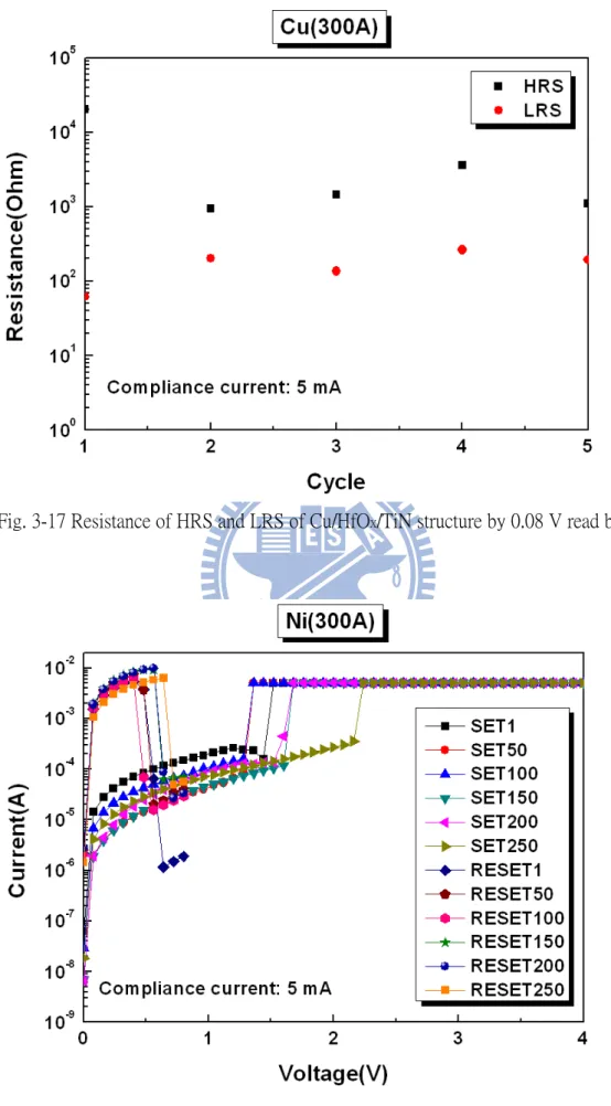
Fig. 3-17 Resistance of HRS and LRS of Cu/HfOX/TiN structure by 0.08 V read bias ...53
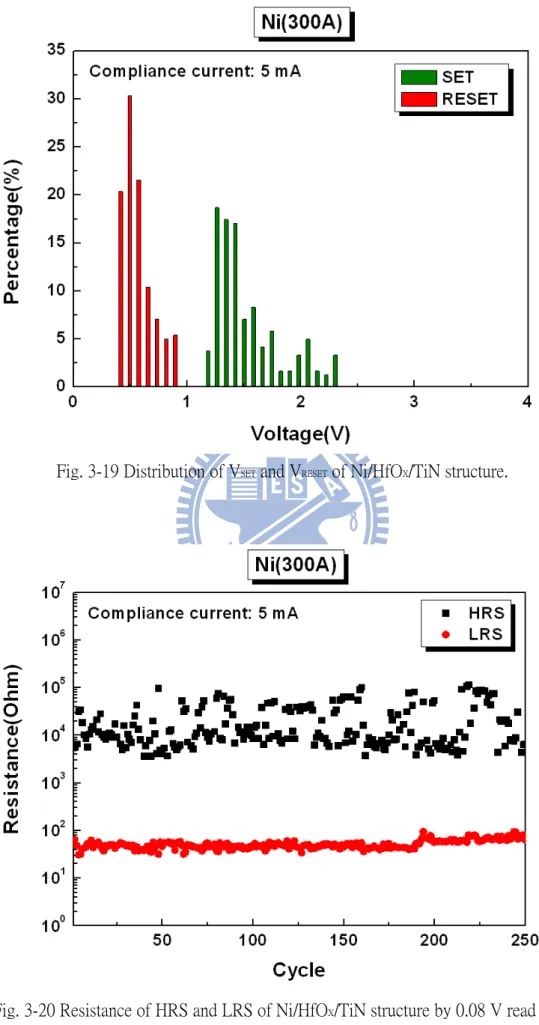
Fig. 3-18 The typical I-V curve of Ni/HfOX/TiN structure ...53
Fig. 3-19 Distribution of VSET and VRESET of Ni/HfOX/TiN structure ...54
Fig. 3-20 Resistance of HRS and LRS of Ni/HfOX/TiN structure by 0.08 V read bias ...54
Fig. 3-21 The typical I-V curve of Ti/HfOX/TiN structure ...55
Fig. 3-22 Distribution of VSET and VRESET of Ti/HfOX/TiN structure ...55
Fig. 3-23 Resistance of HRS and LRS of Ti/HfOX/TiN structure by 0.08 V read bias. ...56
Fig. 3-24 Forming process of Al/HfOX/TiN structure ...56
Fig. 3-25 RESET process of Al/HfOX/TiN structure ...57
Fig. 3-26 Ellingham diagram of representative high-κ dielectrics showing the free energy of formation as a function of temperature ...57 Fig. 3-27 Ellingham diagram plotting the standard free energies of the formation of
oxides of the metals ...58 Fig. 3-28 The typical I-V curve of Pd/HfOX/TiN structure with N2 6 sccm 30 second ....59
Fig. 3-29 Distribution of VSET and VRESET of Pd/HfOX/TiN structure with N2 6 sccm 30
second ...59 Fig. 3-30 Resistance of HRS and LRS of Pd/HfOX/TiN structure with N2 6 sccm 30
second by 0.08 V read bias ...60 Fig. 3-31 The typical I-V curve of TiN/HfOX/TiN structure ...60
Fig. 3-32 Distribution of VSET and VRESET of TiN/HfOX/TiN structure ...61
Fig. 3-33 Resistance of HRS and LRS of TiN/HfOX/TiN structure by 0.08 V read bias .61
Fig. 3-34 The typical I-V curve of Pd/Al(20 Å)/HfOX/TiN structure ...62
Fig. 3-36 Resistance of HRS and LRS of Pd/Al(20 Å)/HfOX/TiN structure by 0.08 V
read bias ...63 Fig. 3-37 The typical I-V curve of Pd/Al(50 Å)/HfOX/TiN structure ...63
Fig. 3-38 Distribution of VSET and VRESET of Pd/Al(50 Å)/HfOX/TiN structure ...64
Fig. 3-39 Resistance of HRS and LRS of Pd/Al(50 Å)/HfOX/TiN structure by 0.08 V
read bias ...64 Fig. 3-40 The typical I-V curve of Pd/Al(75 Å)/HfOX/TiN structure ...65
Fig. 3-41 Distribution of VSET and VRESET of Pd/Al(75 Å)/HfOX/TiN structure ...65
Fig. 3-42 Resistance of HRS and LRS of Pd/Al(75 Å)/HfOX/TiN structure by 0.08 V
read bias ...66 Fig. 3-43 The typical I-V curve of Pd/Al(100 Å)/HfOX/TiN structure ...66
Fig. 3-44 Distribution of VSET and VRESET of Pd/Al(100 Å)/HfOX/TiN structure. ...67
Fig. 3-45 Resistance of HRS and LRS of Pd/Al(100 Å)/HfOX/TiN structure by 0.08 V
read bias ...67 Fig. 3-46 The typical I-V curve of Pd/Al(150 Å)/HfOX/TiN structure for SET process ..68
Fig. 3-47 The typical I-V curve of Pd/Al(150 Å)/HfOX/TiN structure for RESET process
...68 Fig. 3-48 The typical I-V curve of Al/HfOX/TiN structure for etching Al to 30 Å ...69
Fig. 3-49 Distribution of VSET and VRESET of Al/HfOX/TiN structure for etching Al to 30 Å
...69 Fig. 3-50 Resistance of HRS and LRS of Al/HfOX/TiN structure for etching Al to 30 Å
by 0.08 V read bias. ...70 Fig. 3-51 The typical I-V curve of Al(30 Å)/HfOX/TiN structure. ...70
Fig. 3-52 Distribution of VSET and VRESET of Al(30 Å)/HfOX/TiN structure. ...71
Fig. 3-53 Resistance of HRS and LRS of Al(30 Å)/HfOX/TiN structure by 0.08 V read
bias ...71 Fig. 3-54 The typical I-V curve of Pd/Al(35 Å)/HfOX/TiN structure (1~2650 cycles) ....72
Fig. 3-55 The typical I-V curve of Pd/Al(35 Å)/HfOX/TiN structure (2651~4000 cycles)
...72 Fig. 3-56 Distribution of VSET and VRESET of Pd/Al(35 Å)/HfOX/TiN structure (1~2650
cycles) ...73 Fig. 3-57 Distribution of VSET and VRESET of Pd/Al(35 Å)/HfOX/TiN structure (2651~4000
cycles) ...73 Fig. 3-58 Resistance of HRS and LRS of Pd/Al(35 Å)/HfOX/TiN structure by 0.08 V
read bias ...74 Fig. 3-59 Retention time of Pd/HfOX/TiN structure at 85 ℃ by 0.08 V read bias ...74
Fig. 3-60 Retention time of Pd/Al(35 Å)/HfOX/TiN structure at 175 ℃ by 0.08 V read
Fig. 3-61 Temperature dependence of LRS at low to median bias ...75
Fig. 3-62 Temperature dependence of HRS at low to median bias ...76
Fig. 3-63 I-V curve fitting of LRS ...76
Fig. 3-64 I-V curve fitting of HRS at small bias region ...77
Fig. 3-65 I-V curve fitting of HRS at large bias region ...77
Fig. 3-66 XPS intensity of Pd/Al/HfOX/TiN structure ...78
Fig. 3-67 XPS atomic concentration of Pd/Al/HfOX/TiN structure ...78
Fig. 3-68 XPS binding energy of Al/HfOX interface ...79
Fig. 3-69 TEM micrograth of Pd/Al/HfOX/TiN/Ti/SiO2/Si structure ...79
Fig. 3-70 High resolution TEM image of Al/HfOX interface ...80
Fig. 3-71 EDS analysis of the Al layer ...80
Fig. 3-72 The typical I-V curve of Pd/Ti(30 Å)/HfOX/TiN structure ...81
Fig. 3-73 Distribution of VSET and VRESET of Pd/Ti(30 Å)/HfOX/TiN structure ...81
Fig. 3-74 Resistance of HRS and LRS of Pd/Ti(30 Å)/HfOX/TiN structure by 0.08 V read bias ...82
Fig. 3-75 The typical I-V curve of Pt/Ti(30 Å)/HfOX/TiN structure ...82
Fig. 3-76 Distribution of VSET and VRESET of Pt/Ti(30 Å)/HfOX/TiN structure ...83
Fig. 3-77 Resistance of HRS and LRS of Pt/Ti(30 Å)/HfOX/TiN structure by 0.08 V read bias ...83
Fig. 3-78 Retention time of Pt/Ti(30 Å)/HfOX/TiN structure at 85 ℃ by 0.08 V read bias ...84
Fig. 3-79 I-V curve fitting of LRS of Pt/Ti(30 Å)/HfOX/TiN structure. ...84
Fig. 3-80 I-V curve fitting of HRS of Pt/Ti(30 Å)/HfOX/TiN structure at small bias region. ...85
Fig. 3-81 I-V curve fitting of HRS of Pt/Ti(30 Å)/HfOX/TiN structure at large bias region ...85
Fig. 3-82 XPS intensity of Pt/Ti/HfOX/TiN structure ...86
Fig. 3-83 XPS atomic concentration of Pt/Ti/HfOX/TiN structure ...86
Chapter 1 Introduction
1.1 Introduction to nonvolatile memory
The nonvolatile memory (NVM) should keep the stored information without power supply for a long time. In 1967, D. Kahng and S. M. Sze invented the floating-gate nonvolatile semiconductor memory at Bell Labs. In recent years, the portable electronic products can provide the convenient life for human. Therefore, the popularity of portable equipment, such as mobile phone, digital camera, mp3 player, and personal digital assistant, the requirements of NVMs increase significantly in the semiconductor industry. An ideal NVM includes the properties of low operation voltage, simple structure, low power consumption, non-destructive readout, high operation speed, long retention time, high endurance, and small cell size. However, there is no such NVM meet the above properties up to now.
Nowadays, the mainstream of NVM is flash memory, included the NOR flash and NAND flash. The NOR flash has high operation speed, which is suitable for the computer coding, PC bios, DVD player, and mobile phone applications. On the other hand, the NAND flash with higher density is used for large data storage application, such as PDA, memory cards, MP3 players, digital cameras, and USB flash personal disc etc. A primary structure of flash memory is basic on a MOSFET with a modified stacking gate which composed by control gate, dielectric, floating gate and dielectric as a sandwich structure, shown in Fig. 1-1. The logic high or low is determined by charges injected in the floating-gate are maintained there, allowing the difference between threshold voltages of the cell transistor for NVM application.
However, the flash memory has some issues such as high operation voltage, low operation speed, poor retention time, and coupling interference effect during scaling down [1]-[2]. Therefore, some modified flash memories, such as charge-trapping (SONOS) flash and band-engineered SONOS flash are proposed to replace the tradition flash memory [3]-[4]. Moreover, many researchers want to find emerging next-generation NVM with the advantages of DRAM, SRAM, and flash memory. Some possible candidates for next-generation NVMs, including ferroelectric random access memory (FeRAM) [5]-[7], magnetroresistive random access memory (MRAM) [8]-[10], phase change random access memory (PCRAM) [11]-[15], and resistive random access memory (RRAM) are discussed in the next section.
1.2 Introduction to next-generation nonvolatile memories
1.2.1
Ferroelectric Random Access Memory
A ferroelectric material with a spontaneous polarization and the polarization can being altered by applying an electric field. A standard structure of the ferroelectric material is the ABO3 structure (perovskite structures) as shown in Fig. 1-2, where the A, B, and O
atoms are located at corner, body center, and face center of the cubic, respectively. When an electric field is applied to the ferroelectric material, the B atom with two thermodynamically stable positions is located depended on the polarity of the applied electric field. The polarization hysteresis curve of the ferroelectric material is shown in Fig. 1-3. The hysteresis phenomenon of ferroelectric material can be used for NVM applications called it FeRAM. The FeRAM can be subdivided into two types. One type is the metal-ferroelectric-semiconductor FET (MFSFET) structure as shown in Fig. 1-4. The structure is very similar to the MOSFET except the oxide film is replaced by the
ferroelectric film. The polarizations (+Pr or –Pr) of the ferroelectric film will affect the drain current of the transistor, and the memory effect of the MFSFET type FeRAM is nonvolatile and with nondestructive readout property. The other type is similar to DRAM, where the dielectric of the capacitor is replaced by the ferroelectric film. The polarizations of the ferroelectric film will also affect the current of the device. The memory effect of this type FeRAM is also nonvolatile, but the read process is destructive and needing a re-write process.
1.2.2
Magnetroresistive Random Access Memory
The standard MRAM cell is the magnetic tunneling junction which consists of two magnetic layers sandwiching a thin tunneling layer as shown in Fig. 1-5. The magnetization of one magnetic layer, also named reference layer, is fixed and kept in a specific direction. The other layer, also named storage layer, can be switched to parallel or antiparallel to the reference layer by applying a specific magnetic field. The logic high or low is determined by the resistance of parallel or antiparallel state. In read process, a small current flowing through the tunneling layer is detected to recognize the resistance states. The MRAM have a lot of merits, but the reliability of the tunneling layer and the device scaling limitation are the most important challenge of MRAM.
1.2.3
Phase Change Random Access Memory
A phase-change memory (PCRAM), also named ovonic unified memory (OUM), is reported by Neale et al. in 1970. The standard memory cell of PCRAM is shown in Fig. 1-6 [12], where the GeSbTe (GST) chalcogenide alloy material has been adopted as a primary material of the PCRAM. The PCRAM exhibits two different structural phases of
the GST, amorphous and polycrystalline, for data storage. In reset process, a high magnitude current pulse with short tailing edge is applied on the programmable volume of the phase change material. The temperature of the material exceeds the melting point which eliminates the polycrystalline order in the volume. When the reset pulse is terminated, the device quenches to “freeze in" the disordered structural state. This quench time about several nanoseconds is determined by the thermal environment of the device and the fall time of the reset pulse. In set process, a moderate magnitude current pulse with sufficient duration is applied to maintain the device temperature for crystal growth. The amorphous structural state (high resistance state) or the polycrystalline structural state (low resistance state) is read by applying a low magnitude and long duration current pulse. The time-temperature relationship of the PCRAM is shown in Fig. 1-7 [12]. During the set and reset processes, large Joule heating is applied on the phase change material, and hence, huge power is consumed. How to reduce the power consumption during the PCRAM operation is a significant challenge of the PCRAM.
1.2.4
Resistive Random Access Memory
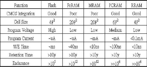
The resistive random access memory which consists of two memory states, the low resistance state (LRS) and the high resistance state (HRS), which can be altered by applying bias voltage or pulse, and utilizes the two different resistance values to storage digital data. Table 1-1 performs the comparison with the Flash and next-generation NVMs [16]-[17]. This table shows that the RRAM with low operation voltage and power, high operation speed, high scalability, good endurance, small size, etc. The details of the RRAM are discussed in section.
1.3 Introduction to Resistive Random Access Memory
1.3.1
Forming process and resistive switching polarities
The forming process is the common phenomenon in the binary metal oxide films which is similar to the dielectric breakdown, named it “soft breakdown". Forming is possible with structures containing a wide variety of amorphous or microcrystalline insulators between a few tens and many hundreds of nanometers thick and a variety of metal electrodes, although the process occurs most readily when noble metals (such as Au) are used as the anode material. The forming voltage is strongly dependent upon the dielectric or its thickness. The cathode material does not affect the forming process or subsequent properties. Therefore, the anode of the resistive switching device plays an important role in the forming process and diffuses into the resistive switching film to change the resistivity considerably.
The resistive switching properties can be divided into three types based on the resistive switching polarities. First, the resistive switching is defined as unipolar resistive switching when being performed only by one polarity of the applied voltage bias, as indicated in Fig. 1-8 (a) [18]. Second, As for bipolar resistive switching, it depicts that the resistive switching phenomenon is observed as applying the specific polarity of the voltage and current biases to reach the ON-state, and back into the OFF-state by applying the other polarity of the voltage and current biases as shown in Fig. 1-8 (b) [18]. Third, Fig. 1-9 [19] shows the typical I-V curve of nonpolar resistive switching. Nonpolar switching means that the device can be switched to another state by applying an electric signal regardless of the directions.
1.3.2
Top electrodes
Because the RRAM stores the digital data by different resistance value, the resistive switching behavior might result from the resistance change at Metal-Insulator interface. Thus, the different work function, electronegativity, and oxygen affinity property of metal, even the interface reaction, and the interdiffusion all possibly have influence on the resistive switching behaviors. Therefore, to make RRAM more practical and reliable, it is very important to pick up the suitable combination of the electrodes.
1.3.3
Resistive switching films
The resistive switching phenomena have been found in many materials. The research mainstream is focused on several groups, including binary oxides, complex metal oxide, perovskite oxides, manganites, and other alloy or polymers.
The binary metal oxides such as NiO, TiO2, HfO2, and etc [20]-[22]. The complex
metal materials such as Gd1-xCaxBaCo2O5, Ba0.7Sr0.3TiO3, and etc. The carrier-doped
manganites with the perovskite structure, such as Pr1-xCaxMnO3 (PCMO), La1-xCaxMnO3
(LCMO), and etc.
Various processing techniques can be used for the preparation of composite and multilayer resistive switching thin films by modifying the apparatus and the conditions for deposition, such as atomic layer deposition (ALD), electron cyclotron resonance (ECR) sputtering, plasma-enhanced atomic layer deposition (PEALD), plasma-enhanced chemical vapor deposition (PECVD), pulsed laser deposition (PLD), metallorganic chemical vapor deposition (MOCVD), reactive DC sputtering, RF sputtering, sol-gel method, and solid-state reaction method.
working process are introduced to elucidate the influence on the resistive switching properties. In addition, the dopant species and the crystallinity of the resistive switching films also determine the resistive switching behaviors, which have been discussed as well.
1.4 Conduction mechanisms
The resistive switching mechanisms of each RRAM material are not clearly understood up to now. Therefore, the conduction mechanisms of each resistance state of the RRAM device are studied for further understanding of the resistive switching mechanisms in each RRAM material. In this section, six basic conduction mechanisms in insulator are summarized in Table 1-2 [94].
1.4.1
Schottky emission
The Schottky emission is caused by thermionic emission of carriers across the interface between metal and insulator [94]. Therefore, the Schottky emission is also named it thermionic emission. If carriers transport in an insulator is by this mechanism, a plot of Ln|J/T2
| versus 1/T in a specific voltage is a straight line, and the slope can determine the permittivity of the insulator. Besides, a lot of Ln|J| versus V1/2
at a fixed temperature is also a straight line.
1.4.2
Frenkel-Poole emission
The Frenkel-Poole (F-P) emission is due to field-enhance thermal excitation of trapped electrons into the conduction band [94]. For the F-P emission, plots of Ln|J| versus 1/T in a specific voltage and Ln|J/V| versus V1/2
1.4.3
Tunnel or Field emission
The tunnel or field emission corresponds to electrons tunneling from the metal Fermi energy into the insulator conduction band or field ionization of trapped electrons into the conduction band [94]. This emission is strongly dependent on the applied voltage, but is essentially independent on the temperature. A plot of Ln|J/V2
| versus 1/V is a straight line in this conduction mechanism.
1.4.4
Space-charge-limited current
The space-charge-limited current (SCLC) is caused by carriers injected into the insulator and no compensation charge is present [94]. The density of SCLC is direct proportion to V2
, and is essentially independent on the temperature.
1.4.5
Ohmic conduction
The Ohmic conduction is results from thermally excited electrons hopping from one isolated state to the next state [94]. If carriers transport in an insulator is by this conduction, plots of Ln|J| versus Ln|V| at fixed temperature and Ln|J| versus 1/T in a specific voltage are straight lines with unity slope.
1.4.6
Ionic conduction
The ionic conduction is similar to a diffusion process. In this mechanism, the voltage and current dependence is the same with the Ohmic conduction at a fixed temperature, and a plot of Ln|J T| versus 1/T in a specific voltage is a straight line with unity slope. In addition, each conduction mechanism may dominate in some voltage and temperature
ranges, and there are possibly two or more mechanisms causing the conduction in an insulator.
1.5 Filament model
The major possible models having been proposed by other research groups are sorted as the following, including filament model, charge tapping and detrapping model, phase change, and solid-state electrolyte. Each model may be applied for some combinations of electrodes and oxide materials. However, many models were proposed by many researchers up to now, but the mainstream of many models nowadays is filament model [23]-[29].
The filamentary model comes from the nature of oxide breakdown and integrity that the defects existing in an oxide bulk such as the interstitials and vacancies of oxygen and metals constitute the leakage current path, as depicted in Fig. 1-10 [30]. This model has been proposed since 1970's and is one of the earliest models in resistive switching. Recently, since nonvolatile memories have acquired a lot of attention, the further and more detailed studies have been carried out to investigate the possible resistive switching mechanisms. The most obvious evidences for the filamentary model are conductive atomic force microscopy (CAFM) mapping results and the cell-area-insensitivity of LRS and HRS, as shown Fig. 1-11 [31]. CAFM is one of the best tools to investigate the local conductivity throughout the film.
Another subject of debate this model is the switching process. It is reasonable to assume that the oxygen deficient region (filaments) of a film is much more conducting than the stoichiometric region irrespective of whatever the defect type is. Generally the mobility of oxygen ions in binary oxides is much higher than metal ions, and the formation of the filaments could be induced by the rejection of O
process, it is the electrical field effect that takes an essential part, because the insulating parts among the filaments are stressed by the highest electrical field accompanied with point discharge effect. As for the filament rupture, it is the current-induced effect that rules the process in which Joule heating effect resulting from the current flow through the tiny filaments generates heat and raises temperature up to hundreds of degree Celsius at the local spot, providing enough energy for oxygen ions to reflow and making the conductive regions of non-stoichiometry return to insulator to rupture the filaments.
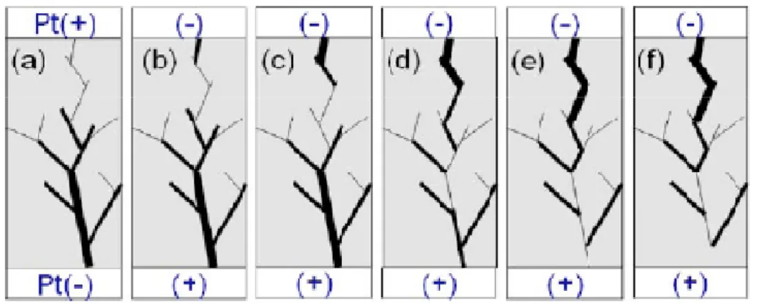
Recently, the concept of tree-shaped filament structure has been proposed. The breakdown paths (filaments) are formed in a dielectric when the carriers are injected from a local point at the electrode interface. The initial cross-sectional area of the path for the carrier conduction is quite narrow, but with the propagation of the filaments the cross section largely increases by an increasing number of secondary formed paths. Therefore the region near the cathode might contain filaments with a larger conductivity compared to the region near the anode. That is to say the filament is thick at the cathode and thin at the anode if merely considering a single filament, which matters in terms of conductivity and has impact on Joule heating effect. It is at the thinnest part of a filament near the anode that most thermal energy accumulates and the filament formation and rupture occur. Experiments reported by K. M. Kim et al. show that only 3~10 nm of the filaments near the anode dominates the switching, and the schematics are shown in Fig. 1-12 [32].
Table 1-1 Comparison with the Flash memory and next-generation NVMs.
Fig. 1-1 Typical floating-gate flash memory.
Fig. 1-2 ABO3 structure (perovskite structures).
Fig. 1-4 MFSFET structure of the FeRAM.
Fig. 1-5 Parallel state (low resistance state) and antiparallel state (high resistance state) of the MRAM.
Fig. 1-6 Basic memory cell of the PCRAM [12].
Fig. 1-8 (a) Typical I-V curves of the unipolar resistive switching. (b) Typical I-V curves of the bipolar resistive switching [18].
Fig. 1-10 Schematic of the filament in an oxide [30].
(a)
(b)
Fig. 1-12 Schematic diagram for switching from LRS to HRS. (a) LRS formed by positive bias on TE. [(b)-(e)] Nucleation and propagation of a filament when negative bias is
Chapter 2 Experiment Details
2.1 Experimental procedure
Resistive memory device were fabricated as follows [33]-[36]. TiN metal as a bottom electrode was deposited on Ti/SiO2/Si wafer by sputtering. Then, nonstoichiometric HfOX
films with a thickness of 20 nm were deposited by ALD (ASM, Polygon 8200) at temperature of 300 O
C. Hafnium tetrachloride (HfCl4) and water (H2O) were used as
reactants for HfOX deposition, and changed the aspect ratio to 2:5. The primitive
chemical-formula as follows [37]-[39].
HfCl4 + 4H2O → Hf(OH)4 + HCl↑ (2-1)
Hf(OH)4 heating → HfO2 + H2O (2-2)
After stacking HfOX thin films on the bottom electrodes, various kind of metals as top
electrodes were deposited by sputtering using a shadow mask at room temperature, such as Pt, Pd, Cu, Ni, Ti, Al, and etc. The thickness of metals were about 30-100 nm. To study the area dependence of the electrical properties, the circular top electrodes were formed with diameters of 100 μm. The structure of device shown in Fig. 2-1. The surface morphology of HfOX/TiN/Ti/SiO2/Si samples was examined by atomic force microscopy
(AFM) in trapping mode, and the composition depth profiles of HfOX films were carried
out by X-ray photon-electron spectroscopy (XPS).
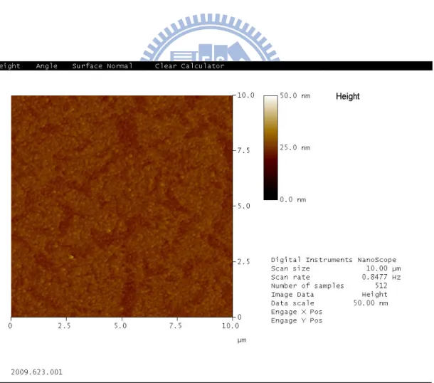
As shown in Fig. 2-2, and Fig. 2-3, the rms surface roughness over a scanning area of 10 10μm2
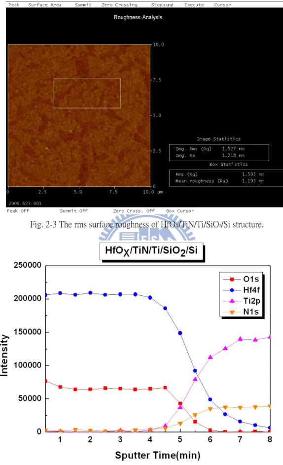
is around 1.5 nm. The depth profile of the chemical composition of HfOX
films measured by XPS is shown Fig. 2-4, and Fig. 2-5. The atomic ratio of oxygen to hafnium (O:Hf) inside the HfOX film is found to be about 1.5, which suggests that the
HfOX film is nonstoichiometric. The binding energy of HfOX films measured by XPS is
shown Fig. 2-6. The primitive binding energy of HfO2 is 16.7 eV. The peak of plot is shift,
and peak of Hf7/2 and Hf5/2 is not very clear, which was demonstrated the resistive switching
films is nonstoichiometric HfOX films. In addition, residual chloride in our HfOX film,
which was used in the ALD process as a chloride precursor (HfCl4), was not detected by
XPS measurement.
2.2 Material analyses
Many material analyses are used to assist us in understanding the related and the corresponding electrical properties to investigate the dopant effects, the top electrode effects, and the resistive switching mechanism. Atomic force microscopy, X-ray photoelectron spectrometer, Focus Ion Beam, and Transmission electron microscopy are used in the thesis, which are going to be introduced in the following content.
2.2.1
Atomic force microscopy
The surface roughness and surface morphology of the bottom electrodes and the resistive switching thin films are characterized by the atomic force microscopy in tapping mode. The average roughness (Ra) and the root mean square (RMS) roughness of the
device are automatically recorded and calculated by the software.
2.2.2
X-ray photoelectron spectroscopy
When the light illuminates the matter, the inner electrons are going to be excited and ionized. The ionized electrons, which close to the surface of the matter, have the ability to
escape into vacuum, named photoelectron, and the phenomenon is called photoelectric effect. Due to the different components and chemical states of the matters, photoelectrons have characteristic kinetic energy, which can be used to identify the composed elements and the chemical states of surface atoms. When the excitation source is soft x-ray, the photoemission spectroscopy is termed by X-ray photoelectron spectroscopy.
2.2.3
Focus ion beam
FIB is a scientific instrument that resembles a scanning electron microscope. However, the SEM uses a focused beam of electrons to image the sample in the chamber, whereas a FIB instead uses a focused beam of gallium ions. Gallium is chosen because it is easy to build a gallium liquid metal ion source (LMIS). In a Gallium LMIS, gallium metal is placed in contact with a tungsten needle and heated. Gallium wets the tungsten, and a huge electric field (greater than 108
V per centimeter) causes ionization and field emission of the gallium atoms.
Unlike an electron microscope, the FIB is inherently destructive to the specimen. When the high-energy gallium ions strike the sample, they will sputter atoms from the surface. Gallium atoms will also be implanted into the top few nanometers of the surface, and the surface will be made amorphous.
Because of the sputtering capability, the FIB is used as a micro-machining tool, to modify or machine materials at the micro- and nano-scale.
The FIB is commonly used to prepare samples for the transmission electron microscope. The TEM requires very thin samples, typically ~100 nanometers. The nanometer-scale resolution of the FIB allows the exact thin region to be chosen.
2.2.4
Transmission electron microscopy and Energy dispersive
spectroscopy
Transmission electron microscopy (TEM) is a microscopy technique whereby a beam of electrons is transmitted through an ultra thin specimen, interacting with the specimen as it passes through it. An image is formed from the electrons transmitted through the specimen, magnified and focused by an objective lens and appears on an imaging screen, a fluorescent screen in most TEMs, plus a monitor, or on a layer of photographic film, or to be detected by a sensor such as a CCD camera.
In material science/metallurgy the speciments tend to be naturally resistant to vacuum, but must be prepared as a thin foil, or etched so some portion of the specimen is thin enough for the beam to penetrate. Preparation techniques to obtain an electron transparent region include ion beam milling and wedge polishing. The focused ion beam (FIB) is a relatively new technique to prepare thin samples for TEM examination from larger specimens. Because the FIB can be used to micro-machine samples very precisely, it is possible to mill very thin membranes from a specific area of a sample, such as a semiconductor or metal.
By the way, TEM and EDS can be analyzed at the same time. Energy dispersive spectroscopy (EDS) analysis, it is released X-ray that the components percentage of the sample is analyzed by electron hit the surface of TEM sample.
2.3 Electrical measurements
The most important parts of all are the electrical measurements. The electrical properties of the devices from I-V curve are demonstrated. The electrical measurement system consisted of a probe station, an Agilent 4156C semiconductor parameter analyzer,
and GPIB controller.
Our electrical measurement was sorted into three items: current-voltage measurement by DC voltage sweeping, endurance measurement, and data retention time measurement. The three initial items are tested for criteria of our memory devices.
2.3.1
Current-voltage measurement
The measurement is performed by Agilent 4156C which provides a DC voltage sweeping between two specific voltages to observe the resistive switching. We could observe the relations between the bias voltage and the current of the high/low resistive states.
2.3.2
Endurance measurement
Before used in commercial applications, it is important to investigate that how many times that the memory devices can be operated before failure. That is so called endurance measurement. A memory device is expected with excellent endurance characteristics due to the requirements for users.
2.3.3
Data retention time measurement
Retention time is how long the stored data can be maintained, and the data is not able to be distinguished beyond retention time. The data retention time measurement is performed by reading the stored data after certain periods to find out if there occurs data loss or not. The data retention time measurement performed at high temperature can accelerate the degradation of the device to investigate the thermal stability of the memory
Fig. 2-1 The device structure of our sample.
Fig. 2-3 The rms surface roughness of HfOX/TiN/Ti/SiO2/Si structure.
Fig. 2-5 XPS atomic concentration of HfOX/TiN/Ti/SiO2/Si structure.
Chapter 3 Results and Discussion
3.1 Defined some resistive switching parameters
3.1.1 Resistive switching parameters
First, we have been defining some resistive switching parameters. In Fig. 3-1, the unipolar resistive switching is performed by sweeping current bias. The forming process is the common phenomenon in the binary metal oxide films which is similar to the dielectric breakdown, named it “soft breakdown". In general, exhibits two memory states: the low resistance state (LRS), also named high conducting state (ON-state) and the high resistance state (HRS), also named low conducting state (OFF-state), which can be altered by applying bias voltage, and utilizes the two different resistance values to storage digital data. RHRS (Roff) is defined the resistance of HRS. RLRS (Ron) is defined the resistance of LRS. ON
process is defined as the transformation from LRS into HRS. OFF process is defined as the transformation from HRS into LRS. VSET (Von) is the voltage which is the highest slope of
current-voltage curve. During ON process, a sudden increase in current occurs at VSET and
limited at compliance current. VRESET (VOFF) is the voltage which the lowest slope of
current-voltage curve. During OFF process, a sudden decrease in current occurs at VRESET.
3.1.2 Compliance current
An important part of RRAM is the compliance current [40]-[44]. Compliance current imposed by the measure instruments or the electrical circuit is imposed on the resistive switching memory device to avoid the device breakdown. To investigate the influence of
compliance current during resistive switching, the compliance currents are varied from µA to mA as shown in Fig. 3-2. As the compliance current of resistive switching reaches 5 µA, the VSET and VRESET values increases and overlap each other, and various resistance of HRS
increases. This phenomenon might be attributed to that because the smaller compliance current forms few filaments which are very weak. The weak filaments are created that is easy to rupture all the filaments at the same time during OFF process, and the weak filaments are more easier to form in other place of HfOX films which leads to the VSET and
VRESET values increases and overlap each other, and resistance of HRS is larger various, as
shown in Fig. 3-2 (a). As the compliance current of resistive switching reaches 5 mA, the VSET and VRESET values decreases and don't overlap each other, and various resistance of
HRS decreases. This phenomenon might be attributed to that because the larger compliance current forms many filaments which are very strong. The strong filaments are created that is hard to rupture all the filaments at the same time during OFF process, and the strong filaments are more easier to form in the residual partial filaments of HfOX films
which leads to the VSET and VRESET values decreases and don't overlap each other, and
resistance of HRS is smaller various, as shown in Fig. 3-2 (b).
3.2 Various metal of top electrodes
In many reports, we know that top electrodes and resistive switching films are great influence on the RRAM [45]-[50]. Therefore, in order to reduce variables, we fixed resistive switching films for HfOX films, then to change the different electrode. In this
section, we performed the resistive switching in various top electrodes/HfOX/TiN/Ti/SiO2/Si devices where various top electrodes where Pt, Pd, Cu, Ni,
3.2.1 Electrical properties of various top electrodes
At this section, we would show the basic memory device electrical properties of various top electrodes, including resistive switching characteristics, distribution of VSET and
VRESET, resistance of HRS and LRS.
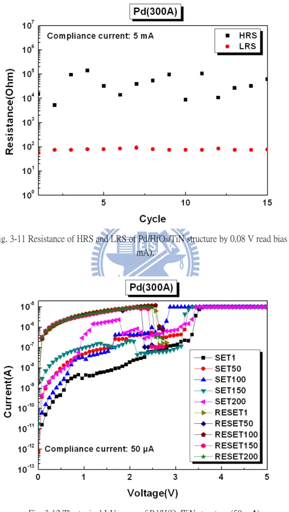
In Pt/HfOX/TiN device, first, is using the dc voltage sweep method with a current
compliance of 5 mA. In Fig. 3-3 shows the typical I-V curve. Distribution of VSET and
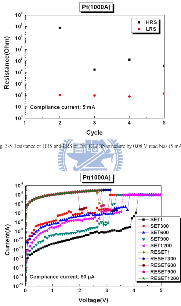
VRESET are shown in Fig. 3-4. Resistance of HRS and LRS by 0.08 V read bias are shown in
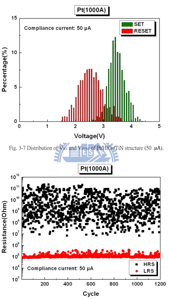
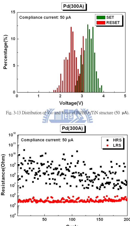
Fig. 3-5. Second, the compliance current changed 50 µA, and shows the typical I-V curve in Fig. 3-6. Distribution of VSET and VRESET are shown in Fig. 3-7. Resistance of HRS and
LRS by 0.08 V read bias are shown in Fig. 3-8. Form the results, we demonstrates when Pt as top electrode, which can use the dc voltage sweep with different compliance current. As mentioned in the previous section, smaller compliance current leads to the VSET and VRESET
values increases and overlap each other, and resistance of HRS is larger various, but the endurance is more than 1200 cycles. On the contrary the lager compliance current leading to the VSET and VRESET values decreases and don't overlap each other, and various
resistance of HRS decreases, but the endurance is less than 15 cycles.
In Pd/HfOX/TiN device, first, is using the dc voltage sweep method with a current
compliance of 5 mA. In Fig. 3-9 shows the typical I-V curve. Distribution of VSET and
VRESET are shown in Fig. 3-10. Resistance of HRS and LRS by 0.08 V read bias are shown
in Fig. 3-11. Second, the compliance current changed 50 µA, and shows the typical I-V curve in Fig. 3-12. Distribution of VSET and VRESET are shown in Fig. 3-13. Resistance of
HRS and LRS by 0.08 V read bias are shown in Fig. 3-14. Form the results, we demonstrates when Pd as top electrode, which can use the dc voltage sweep with different compliance current. As mentioned in the previous section, smaller compliance current leading to the VSET and VRESET values increases and overlap each other, and resistance of
HRS is larger various, but the endurance is more than 200 cycles. On the contrary the lager compliance current leading to the VSET and VRESET values decreases and don't overlap each
other, and various resistance of HRS decreases, but the endurance is less than 30 cycles. In Cu/HfOX/TiN device, is using the dc voltage sweep method with a current
compliance of 5 mA. In Fig. 3-15 shows the typical I-V curve. Distribution of VSET and
VRESET are shown in Fig. 3-16. Resistance of HRS and LRS by 0.08 V read bias are shown
in Fig. 3-17. Form the results, we demonstrates when Cu as top electrode, which only use the dc voltage sweep with mA compliance current. As mentioned in the previous section, lager compliance current leading to the VSET and VRESET values decreases and don't overlap
each other, and various resistance of HRS decreases, but the endurance is less than 10 cycles.
In Ni/HfOX/TiN device, is using the dc voltage sweep method with a current
compliance of 5 mA. In Fig. 3-18 shows the typical I-V curve. Distribution of VSET and
VRESET are shown in Fig. 3-19. Resistance of HRS and LRS by 0.08 V read bias are shown
in Fig. 3-20. Form the results, we demonstrates when Ni as top electrode, which only use the dc voltage sweep with mA compliance current. As mentioned in the previous section, lager compliance current leading to the VSET and VRESET values decreases and don't overlap
each other, various resistance of HRS decreases, and the endurance is more than 250 cycles.
In Ti/HfOX/TiN device, is using the dc voltage sweep method with a current
compliance of 3 mA. In Fig. 3-21 shows the typical I-V curve. Distribution of VSET and
VRESET are shown in Fig. 3-22. Resistance of HRS and LRS by 0.08 V read bias are shown
in Fig. 3-23. Form the results, we demonstrates when Ti as top electrode, which only use the dc voltage sweep with mA compliance current. As mentioned in the previous section, lager compliance current leading to the VSET and VRESET values decreases and don't overlap
each other, and various resistance of HRS decreases, but the endurance is less than 50 cycles.
In Al/HfOX/TiN device, forming process is formed as shown in Fig. 3-24. After
forming process, the device couldn't cause resistive switching as shown in Fig. 3-25. That is to say the resistive switching phenomenon couldn't be observed for Al/HfOX/TiN
device.
3.2.2 Work function of various metals
According to textbooks, the values of work function φ of various metals are as follows; φPt=5.65 eV, φPd=5.12 eV, φNi=5.15 eV, φCu=4.65 eV, φTi=4.33 eV, and
φAl=4.28 eV.
In the early reports, such as Sawa et al., which proposed that a Schottky barrier, the origin of the nonlinearity of the I-V curve, is formed by a low work function metal and p-type semiconductor PCMO, and the resistive switching mechanism on based Schottky barrier barrier modulation was suggested [51]. Afterward, Seo et al., demonstrated that the effective electric field across the NiO film was high enough to cause resistive switching phenomenon while Ohmic contact or a low Schottky barrier formed between the metal-insulator interface. There is no resistive switching phenomenon with Ti top electrode due to the considerable voltage drop across the well-established Schottky barrier at the Ti/NiO interface [52].
In particular, our sample of various top electrodes did not show similar resistive switching characteristics as reported previously. Table 3-1 performs the comparison with the work function and resistive switching parameters of various metals. We demonstrates larger work function metal, which has better electrical properties, and can resistive switching for different compliance current, but there are different electrical properties on
different compliance current. The work function could not be clear to explain this phenomenon.
3.2.3 Free energy of various metals
Recently, electronegativity and free energy is often used to explain the mechanism RRAM. Hasan et al. proposed that under a positive bias, electromigration of oxygen ions forms thicker oxide, which dissociates under a negative bias, causes high and low resistance states, respectively [53]-[54]. Afterward, Lee et al. proposed that the importance of the reaction at the metal/NiO interface is demonstrated in relation to the free energy of oxide formation of electrode metals and Ni [47], [55]-[57].
Figure 3-26 shows Ellingham diagram of representative high-κ dielectrics showing the free energy of formation as a function of temperature, and Fig. 3-27 shows Ellingham diagram plotting the standard free energies of the formation of oxides of the metals. The free energy of oxidation of Al is close to the free energy of oxidation of Hf. Therefore, the Al/HfOX/TiN device showed no resistive switching characteristics. Because Al attracted
and trapped more oxygen ions from HfOX films to form interface layer [58]-[68], which
resulted the filaments were not ruptured.
The Ti top electrode was investigated, as Ti has slightly larger free energy of oxidation than free energy of oxidation of Hf. Therefore, the Ti/HfOX/TiN device showed
resistive switching characteristics, but the endurance is bad. Because Ti still attracted and trapped some oxygen ions from HfOX films to form thin interface layer. When RESET
process, the filaments were not ruptured clearly. Therefore, resistance of HRS and ratio decrease.
The Ni top electrode was also investigated, as Ni has higher free energy of oxidation than free energy of oxidation of Hf. Therefore, the Ni/HfOX/TiN device showed good
resistive switching characteristics. Because Ni did not attract and trap oxygen ions from HfOX films.
The Cu top electrode was also investigated, as Cu has higher free energy of oxidation than free energy of oxidation of Hf. However, the Cu/HfOX/TiN device showed bad
resistive switching characteristics. Because Cu is a highly diffusive element in semiconductor materials due to its high diffusion coefficient, they could migrate into the NiO bulk from the top electrode and affect the resistive switching characteristics. The formula as follows.
D=D0 exp(-Q/KT) (3-1)
The Pt and Pd top electrodes were also investigated, as Pt and Pd have very high free energy of oxidation than free energy of oxidation of Hf. Therefore, the Pt/HfOX/TiN and
Pd/HfOX/TiN device showed good resistive switching characteristics, and could sweep with
different compliance current. However, sweep with larger compliance current resulted bad endurance. Because Pt and Pd have too higher free energy, when applied a dc voltage, the oxygen ions is direct from HfOX films to air. Table 3-2 performs the comparison with
the free energy of oxide formation of electrode metals and resistive switching parameters of various metals.
In order to confirm our thoughts, we used Pd as top electrode, and injected N2 6 sccm
30 second. In Fig. 3-28 shows the typical I-V curve. Distribution of VSET and VRESET are
shown in Fig. 3-29. Resistance of HRS and LRS by 0.08 V read bias are shown in Fig. 3-30. Form the results, we demonstrates the Pd/HfOX/TiN with N2 showed better resistive
switching characteristics than the Pd/HfOX/TiN without N2. The endurance is significant
addition. Because N2 can block oxygen ions from HfOX films to air.
Afterward, we used TiN as top electrode under a mixed gas atmosphere with a partial pressure of P(Ar) : P(N2 ) = 24 : 9.6. In Fig. 3-31 shows the typical I-V curve. Distribution
of VSET and VRESET are shown in Fig. 3-32. Resistance of HRS and LRS by 0.08 V read bias
are shown in Fig. 3-33. Form the results, we demonstrates the TiN/HfOX/TiN showed
better resistive switching characteristics than the Ti/HfOX/TiN. The endurance is significant
addition. Because TiN did not attract and trap oxygen ions from HfOX films. Table 3-3
performs the comparison with the Pd/HfOX/TiN with N2 versus without N2 and the
Ti/HfOX/TiN versus TiN/HfOX/TiN.
3.3 Resistive switching characteristics of Pd/Al/HfO
X/TiN
structure
In previous discussions, we demonstrates reactive metal (lower free energy of oxidation of the metal) is easier combined with oxygen from resistive switching films and forms metal oxide, which resulted the filaments were not ruptured and no resistive switching characteristics. However, the inert metal (higher free energy of oxidation of the metal) is hard easier combined with oxygen from resistive switching films. Therefore, the inert metal as top electrode has good resistive switching characteristics, but can't resistive switching in larger compliance current. Because inert metal have too higher free energy, when applied a dc voltage, the oxygen ions is direct from HfOX films to air. In this
paper, we have studied to use two-layer metal as top metal, the first layer is inert metal and the second layer is thin reactive metal, such as Pd/Al, Pt/Ti, etc. Because thin reactive metal can trap oxygen ions to form thin interface layer and avoid oxygen ions from HfOX
films to air, and Inert metal is protection reactive metal which avoid to direct contact with air.
3.3.1 Electrical properties
First, we fixed the thickness of Pd for 30nm, and to change the thickness of Al. In Pd/Al(20 Å)/HfOX/TiN device, is using the dc voltage sweep method with a current
compliance of 5 mA. In Fig. 3-34 shows the typical I-V curve. Distribution of VSET and
VRESET are shown in Fig. 3-35. Resistance of HRS and LRS by 0.08 V read bias are shown
in Fig. 3-36. The Pd/Al(20 Å)/HfOX/TiN device shown good resistive switching
characteristics. The VSET and VRESET values don't overlap each other, and the endurance is
more than 300 cycles.
In Pd/Al(50Å)/HfOX/TiN device, is using the dc voltage sweep method with a current
compliance of 5 mA. In Fig. 3-37 shows the typical I-V curve. Distribution of VSET and
VRESET are shown in Fig. 3-38. Resistance of HRS and LRS by 0.08 V read bias are shown
in Fig. 3-39. The Pd/Al(50 Å)/HfOX/TiN device shown good resistive switching
characteristics. The VSET and VRESET values don't overlap each other, and the endurance is
more than 550 cycles.
In Pd/Al(75Å)/HfOX/TiN device, is using the dc voltage sweep method with a current
compliance of 5 mA. In Fig. 3-40 shows the typical I-V curve. Distribution of VSET and
VRESET are shown in Fig. 3-41. Resistance of HRS and LRS by 0.08 V read bias are shown
in Fig. 3-42. The Pd/Al(75 Å)/HfOX/TiN device shown good resistive switching
characteristics. The VSET and VRESET values don't overlap each other, the endurance is
more than 200 cycles, but the yield decreases.
In Pd/Al(100 Å)/HfOX/TiN device, is using the dc voltage sweep method with a
current compliance of 5 mA. In Fig. 3-43 shows the typical I-V curve. Distribution of VSET
and VRESET are shown in Fig. 3-44. Resistance of HRS and LRS by 0.08 V read bias are
shown in Fig. 3-45. The Pd/Al(100 Å)/HfOX/TiN device shown good resistive switching
more than 450 cycles, but the yield decreases.
In Pd/Al(150 Å)/HfOX/TiN device, is using the dc voltage sweep method with a
current compliance of 5 mA. In Fig. 3-46 shows the typical I-V curve for SET process. In Fig. 3-47 shows the typical I-V curve for RESET process. The Pd/Al(150 Å)/HfOX/TiN
device shown bad resistive switching characteristics, the endurance is less than 3 cycles. In Table 3-4 performs the comparison with the different thickness of Al of Pd/Al/HfOX/TiN structure and resistive switching parameters of the devices. Form the
results, we demonstrates Pd/Al/HfOX/TiN structure which has good resistive switching
characteristics, but thickness of Al is thicker to result that the yield and resistance decrease [69]-[70]. Because thickness of Al is thicker, which forms thicker AlOX at Al/HfOX
interface to result the filaments were not ruptured.
In order to confirm our thoughts, we etched aboriginal Al/HfOX/TiN device for
etching Al solution. The proportion of chemical solution is H3PO4 : HNO3 : CH3COOH :
H2O = 50 : 2 : 10 : 9. Afterward, we etched thickness of Al of the device to 30 Å. In Al(30
Å)/HfOX/TiN device, is using the dc voltage sweep method with a current compliance of 5
mA. In Fig. 3-48 shows the typical I-V curve. Distribution of VSET and VRESET are shown in
Fig. 3-49. Resistance of HRS and LRS by 0.08 V read bias are shown in Fig. 3-50. The Al(30 Å)/HfOX/TiN device has resistive switching phenomenon. Afterward, we used direct
sputtering Al 30 Å as top electrode. In Al(30 Å)/HfOX/TiN device, is using the dc voltage
sweep method with a current compliance of 5 mA. In Fig. 3-51 shows the typical I-V curve. Distribution of VSET and VRESET are shown in Fig. 3-52. Resistance of HRS and LRS by 0.08
V read bias are shown in Fig. 3-53. The Al(30 Å)/HfOX/TiN device has resistive switching
phenomenon.
Form the results, we demonstrates thickness of Al is thicker to result that the yield decreases, and thickness of Al is thin, which has resistive switching phenomenon.
However, thickness of Al is too thin to result oxygen ions through AlOX from HfOX films
to air. Therefore, we chosen Pd/Al(35 Å)/HfOX/TiN structure. In Pd/Al(35 Å)/HfOX/TiN
device, is using the dc voltage sweep method with a current compliance of 5 mA and 10mA. In Fig. 3-54 and Fig. 3-55 shows the typical I-V curve. Distribution of VSET and
VRESET are shown in Fig. 3-56 and Fig. 3-57. Resistance of HRS and LRS by 0.08 V read
bias are shown in Fig. 3-58. In Pd/Al(35 Å)/HfOX/TiN device shown very good resistive
switching characteristics. The VSET and VRESET values don't overlap each other, and the
endurance is more than 4000 cycles.
3.3.2 Retention property
For a nonvolatile memory, the data storage time, called retention time, is an important indicator [71]-[77]. It means that how long the stored resistance values can be remained. In order to accelerate the degradation of Pd/HfOX/TiN structure, the retention test is also
tested under the 85℃. As showed in Fig. 3-59, the retention time of the two states is at 1000 seconds and the resistance ratio only over 1 by 0.08 V read bias. Afterward, in order to accelerate the degradation of Pd/Al(35 Å)/HfOX/TiN structure, the retention test is also
tested under the 175℃, as show in Fig. 3-60. Retention time at the high temperature is at least over 5×10⁴
seconds, and the resistance ratio still remains over 50.
3.3.3 Thermal stability
Current transport mechanisms for the LRS and the HRS were analyzed by measuring the I-V curve at the temperature ranging from 25 to 175 ℃. For the LRS, the I-V curve follows Ohm's law and the resistivity of the HfOX films shows slightly negative
by the set process may be responsible for this observation. On the other hand, the I-V curve of the HRS, as shown in Fig. 3-62, has positive and weak temperature dependence at low bias. This positive temperature dependence for the HRS current suggests that the dominant current transport mechanism for the Pd/Al/HfOX/TiN structure during set process
may be tunneling, Schottky emission, or Pool-Frenkel emission. However, we ruled out Schottky emission and Pool-Frenkel emission as possible candidates due to the very weak temperature dependence of the HRS current [36], [78]-[84].
3.3.4 Curve fitting of current-voltage plots
Figure 3-63 and Fig. 3-64 show the plot of ln |J| versus ln |V| of our Pd/Al(35 Å)/HfOX/TiN structure. In the LRS current and HRS current at small bias region, the curve
present Ohmic behavior whose slopes are close to unity. The ln |J/V2
| versus 1/V curve is presented in Fig. 3-65. The linear line with a negative slope at the large bias region of the plot shows that the HRS current at large bias is due to the Fowler-Nordheim (FN) tunneling [36], [85]-[93].
In the fitting curve, the filament model for the resistive switching in the Pd/Al(35 Å)/HfOX/TiN structure can be described as follows: When HfOX films is destroyed during
the forming process, the conductive path is created. An Ohmic current-voltage behavior is observed for devices. As the device was switched back to the HRS, the HfOX films near the
anode is recovered by the partial rupture of filaments near anode/ HfOX films interface.
3.3.5 Material analyses
In order to analyze Al/HfOX interface and provide extra information for the
atomic percentage, binding energy in the samples and the cross section view. The further details are described as below.
The depth profile of the chemical composition of Pd/Al/HfOX structure measured by
XPS is shown in Fig. 3-66 and Fig. 3-67. We could see that O2 and Al at the same depth,
which is formed AlOX at interface. The binding energy of Pd/Al/HfOX structure measured
by XPS is shown Fig. 3-68. The primitive binding energy of Al2O3 is 74.4 eV. The peak of
plot is close to 74.4 eV, which was demonstrated the AlOX is formed at interface.
Figure 3-69 is the TEM micrograth of Pd/Al/HfOX/TiN/Ti/SiO2/Si structure. Fig. 3-70
is high resolution TEM image of Al/HfOX interface, which shows Al thickness from 3.5
nm to 9 nm. Therefore, we could demonstrate AlOX which was formed at Al/HfOX
interface.
Figure 3-71 is EDS analysis of the Al layer, which shows the Al layer has oxygen content. Therefore, we could demonstrate AlOX which was formed at Al/HfOX interface.
3.3.6 Electrical properties of Pd/Ti/HfO
X/TiN structure
In order to validate our argument, we decided to change the reactive metal. The structure is Pd/Ti(30 Å)/HfOX/TiN. In the device, is using the dc voltage sweep method
with a current compliance of 5 mA. In Fig. 3-72 shows the typical I-V curve. Distribution of VSET and VRESET are shown in Fig. 3-73. Resistance of HRS and LRS by 0.08 V read bias
are shown in Fig. 3-74. The Pd/Ti(30Å)/HfOX/TiN device shown good resistive switching
characteristics. The VSET and VRESET values don't overlap each other, and the endurance is