國 立 交 通 大 學
電子工程學系 電子研究所
碩 士 論 文
奈米級金氧半場效電晶體應變矽物理之研究
Strained Silicon Physics
in
Nanoscale MOSFETs
研 究 生:林以唐
指導教授:陳明哲 博士
奈米級金氧半場效電晶體應變矽物理之研究
Strained Silicon Physics
in
Nanoscale MOSFETs
研 究 生:林以唐
Student:Yi-Tang Lin
指導教授:陳明哲博士
Advisor:Dr. Ming-Jer Chen
國 立 交 通 大 學
電子工程學系 電子研究所
碩 士 論 文
A Thesis
Submitted to Department of Electronics Engineering & Institute of Electronics College of Electrical Engineering
National Chiao Tung University in Partial Fulfillment of the Requirements
for the Degree of Master of Science
In
Electronics Engineering July 2008
Hsinchu, Taiwan, Republic of China
奈米級金氧半場效電晶體應變矽物理之研究
研究生:林以唐
指導教授:陳明哲博士
國立交通大學 電子工程學系 電子研究所碩士班
摘要
為了提升 MOSFETs 元件效能及載子遷移率(carrier mobility),在(001) 晶圓 上的單軸縱向(uniaxial longitudinal)及雙軸(biaxial)應變矽製程已被廣泛的應用在 先進的奈米技術中。
在本論文中,首先,為了探討在不同的晶圓方向及不同的應力條件下,是否 能進一步的增高元件效能及降低元件功率,我們將應變張量(strain tensor)表示成 縱向應力(longitudinal stress)、橫向應力(transverse stress)及垂直應力(normal stress) 的函數。接著利用 deformation potential theory 以及 k‧p framework 來分別計算在 三種晶圓方向:(001)、(110)和(111)上及不同的應力條件下,應變矽材料的傳導 帶和價電帶的能帶結構(band structure)、能谷位移(band edge shift)、三維 k 空間 下的等能量面(constant energy surface)、二維能量等高線(2D energy contour),以 及有效質量(effective mass)。另外,額外的垂直晶圓方向應力及橫向應力也被考 慮及計算。利用以上的計算結果來作為分析的工具,我們發現在這些可能的應變 形式中,對 nMOSFETs 來說,在(001)晶圓上的單軸及雙軸伸張應變具有較佳的 增益;而對 pMOSFETs 來說,在(001)和(110)晶圓上的單軸壓縮應變具有較佳的 增益。此外,對 pMOSFETs 來說,在(001) 晶圓上加上額外的橫向伸張應力可以 進一步的增進元件的電導率(conductivity)。 接著,利用計算出來的能帶結構,我們萃取出在(001) 晶圓方向上的單軸及 雙軸應變下的量子化有效質量(quantization effective mass)、二維及三維能態密度
有效質量(2D and 3D density-of-state effective mass)。此外,根據應變下的能帶結 構,我們推導及修正了半導體元件物理中常用的物理表示式,包含材料的費米能 階 (Fermi energy) 、 傳 導 帶 及 價 電 帶 的 有 效 狀 態 密 度 (conduction and valence effective DOS)、本質載子濃度(intrinsic carrier concentration),使其可以繼續延伸 應用到材料內具有應變的情況。同時我們也計算了這些參數在單軸及雙軸應變下 從零到 3GPa 的變化,並提出了合理的物理解釋。以上這些參數在決定材料特性 及元件效能時相當重要。
最後,根據以上的討論,我們建立了一套物理模型及模擬器來評估及計算應 力對 MOSFETs 元件造成的影響,包含平帶電壓(flat-band voltage)、應變下對應 的多晶矽閘極/氧化層/通道截面能帶圖(band diagram)。並將三角形位能井近似法 (triangular potential approximation) 延伸應用到應變矽 MOSFETs 元件中,同時也 考慮閘極及通道均具有應變的情況。此方法可計算出在不同應力條件、外加電壓 及元件參數下介面電場、次能階、反轉層載子濃度及多晶矽閘極/氧化層/通道跨 壓等重要參數。接著,利用 WKB 方法,我們也計算出在(001)晶圓上單軸壓縮應 變對 nMOSFETs 和 pMOSFETs 的閘極直接穿隧電流(gate direct tunneling current) 的影響,模擬結果與實驗數據吻合。
Strained Silicon Physics in
Nanoscale MOSFETs
Student: Yi-Tang Lin
Advisor: Dr. Ming-Jer Chen
Department of Electronics Engineering
& Institute of Electronics
National Chiao Tung University
Abstract
In this work, by using the deformation potential theory for conduction band and the k‧p framework (6×6 Luttinger Hamiltonian) for valence band, the strain-altered band structure (E-k relation), the strain-induced band edge shift, the constant energy surface, and the 2D energy contour have been calculated for various stress conditions on three conventional wafer orientations, (100), (110), and (111). Moreover, the influences of the additional transverse or normal strain have been examined as well.
Next, utilizing the calculated E-k relation, the conventional physical parameters including the quantization effective mass, the 2D DOS Effective mass, and 3D DOS effective mass have been also extracted under uniaxial and biaxial stress on (001) wafer. Then, using the DOS effective masses and strain-induced band edge shifts, the Fermi energy of bulk silicon can be determined as a function of stress and doping concentration. These parameters are significant in calculating the subband energy and carrier density in the channel inversion layer of MOSFETs. In addition, we also evaluated the intrinsic carrier density of bulk silicon under uniaxial and biaxial stress from zero to 3GPa.
Furthermore, we extended and modified the previously developed triangular potential approximation, a self-consistent method that takes the quantum confinement effect in the inversion layer and the conservation of electric flux at the SiO2/Si interface into consideration, for the unstrained MOSFETs to construct the band diagram and physical model for strained counterparts. The method has also been applied to both nMOSFETs and pMOSFETs with corresponding revisions of the physical model. In our model, the stresses for poly gate and channel are allowed to have different magnitude and type.
Finally, applying our model and the extracted physical parameters, we can calculate the interface electric field, subband energy, inversion carrier density, substrate band bending, etc., with various stress conditions, applied voltage and device parameters as inputs. Then, utilizing the WKB approximation, the transmission probability and gate direct tunneling current for various stress conditions can also be evaluated. The simulated results agree with the experimental data of the former works.
Acknowledgement
這篇論文的完成,首先要感謝陳明哲教授二年來的指導與鼓勵。在雜訊與擾 動課程及每週 seminar 和老師的互動中,讓我學習到許多做研究的方法、思考的 方式、以及嚴謹的態度。而在半導體元件物理課程時及擔任助教時與學弟妹的互 動中,也使我獲益良多,對固態領域有了更深入的體悟。另外要感謝謝振宇學長 及梁惕華同學平日極具啟發性的討論,蒐集的 paper 及資料的分享,並一起釐清 了許多觀念,協助我確立研究的方法與方向。同時要感謝李建志學長、許智育學 長、李韋漢學長在課業、生活及研究上的幫助與建議。另外也要感謝張書通教授 所撰寫的程式及簡鶴年同學無私的分享與討論,使我能夠儘快的瞭解這個領域的 關鍵知識與技術。也要感謝呂立方同學在研究用軟體及物理模擬軟體的使用以及 研究經驗的分享;周佳宏、宋東壕、陳彥銘同學平日的討論與幫助;以及湯侑穎 同學在系學會網路組時期、擔任半導體元件物理助教時、以及實驗室事務上的大 力協助。另外也要感謝張智勝經理、李文欽經理和張書通教授在口試及面試時的 指導與建議。最後要感謝我的家人的全力支持,讓我能夠無後顧之憂的專心在研 究之上。 Yi-Tang, Lin August 2008Contents
Chinese Abstract ... i
English Abstract ...iii
Acknowledgement ...v
Contents ... vi
Table Captions... ix
Figure Captions ...x
Chapter 1 Introduction...1
Chapter 2 Strain-altered Band Structures...3
2.1 Introduction...3
2.2 A Review of Mechanics of Materials...3
2.2.1 Stress ...3
2.2.2 Strain ...5
2.2.3 Relationship between Stress and Strain ...6
2.3 Hamiltonian...8
2.3.1 Hamiltonian for Conduction Band (Deformation Potential Theory) ...8
2.3.2 Hamiltonian for Valence Band (k‧p Framework)...9
2.3.2.1 Various Materials (Si/Ge/GaAs) ...11
2.4 Types of Stress and Various Wafer Orientations ...12
2.5 Results and Discussion ...13
2.5.1 Band Structures ...13
2.5.3 Constant Energy Surface...17
2.5.4 Two-dimension Energy Contour in the Plane of Wafer Surface ...17
2.5.5 Advantageous Strains and Wafer Orientations...18
2.5.6 Influences of Additional Transverse or Normal Stress ...21
2.6 Conclusion ...23
Chapter 3 The Properties of Bulk Silicon in the Presence of Stress ...25
3.1 Introduction...25
3.2 Effective Mass ...26
3.3 Carrier Density and Effective DOS ...29
3.3.1 Electrons in Conduction Band ...29
3.3.2 Holes in Valence Band ...30
3.3.3 Simulated Results of NC* and NV* ...31
3.4 Fermi Energy of Bulk Silicon ...31
3.5 Intrinsic Carrier Concentration ...33
3.6 Conclusion ...33
Chapter 4 Strain-induced Change of Gate Direct Tunneling Current...35
4.1 Introduction...35
4.2 Physical Model...36
4.2.1 Hole Subband Energy and Carrier Density (pMOSFETs) ...36
4.2.2 Hole Direct Tunneling Current for pMOSFETs...39
4.2.3 Electron Direct Tunneling Current for nMOSFETs...41
4.3 Results and Discussion ...42
4.3.1.1 Parameters Extraction for the Vertical Electric Field
Component...42
4.3.1.2. Calculation for the Stress Component (Valence Band Edge Shifts)...43
4.3.1.3. Hole Direct Tunneling Current ...44
4.3.1.4 Uniaxial Transverse Stress ...45
4.3.2 Electron Direct Tunneling Current for nMOSFETs...46
4.4 Conclusion ...47
Chapter 5 Conclusions...48
References ...51
Table Captions
Chapter 2
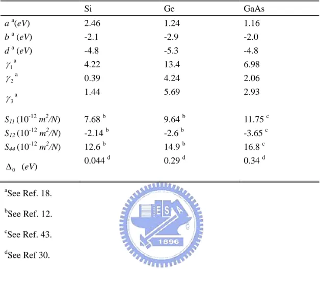
Table 2.1 The deformation potentials, Luttinger parameters, elastic stiffness constants, and split-off energy for Si, Ge, and GaAs. ...55 Table 2.2 The normal, longitudinal, and transverse direction for (001), (110), and (111)
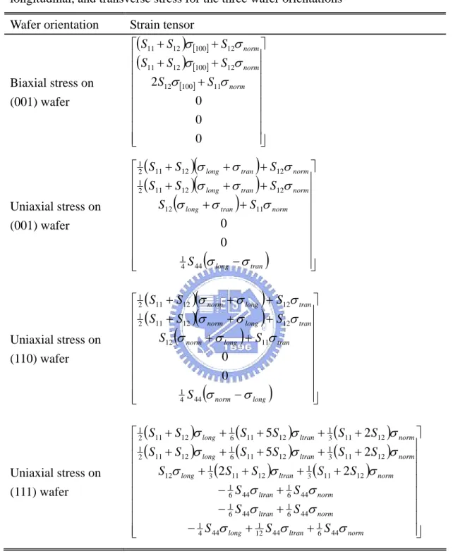
wafer. ...56 Table 2.3 The stress tensor and strain tensor for biaxial stress on (001) wafer, uniaxial stress along [110], [110], [001], [111], and [11 2 ] direction...57 Table 2.4 The resultant strain tensors in response to the combination of normal,
longitudinal, and transverse stress for the three wafer orientations. ...58 Table 2.5 Numerical values of effective mass for silicon conduction band in inversion layer given by [30]. ...59 Table 2.6 The conductivity, transverse, and quantization effective masses of the top
band for bulk silicon with various stress conditions and wafer orientations. The quantization effective masses of the second band are also listed...60 Table 2.7 Comparison the effective masses between the 1GPa uniaxial longitudinal
compressive stress with and without additional 1GPa uniaxial transverse tensile stress for (001) and (110) wafer. ...61
Chapter 4
Figure Captions
Chapter 2
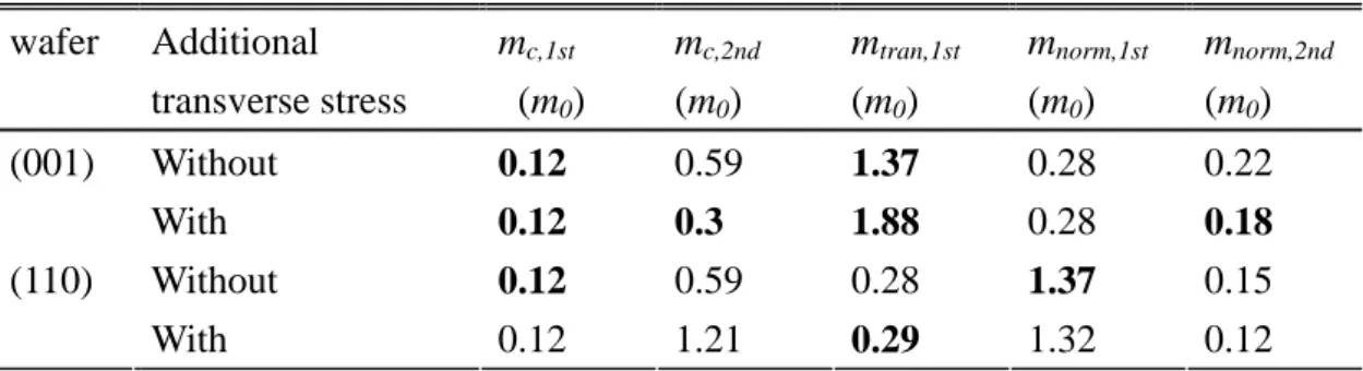
Fig. 2.1.. (a) An arbitrary force ΔR
( )
P acting on an infinitesimal area Δ at point P. AThe normal component of the force is ΔF
( )
P and the tangential components of the force are ΔVs( )
P and ΔVt( )
P along two orthogonal directions in the plane. (b) Schematic of the nine components defining the stress state at an arbitrary point in three dimensions...63 Fig. 2.2. (a) Schematic of the deformation of a body applied to normal stress alongy-axis; and (b) schematic the deformation of a body applied to pure shear stress. Dash line indicates the size and shape of the original body before deformation and solid line indicates those of the body after deformation. ....
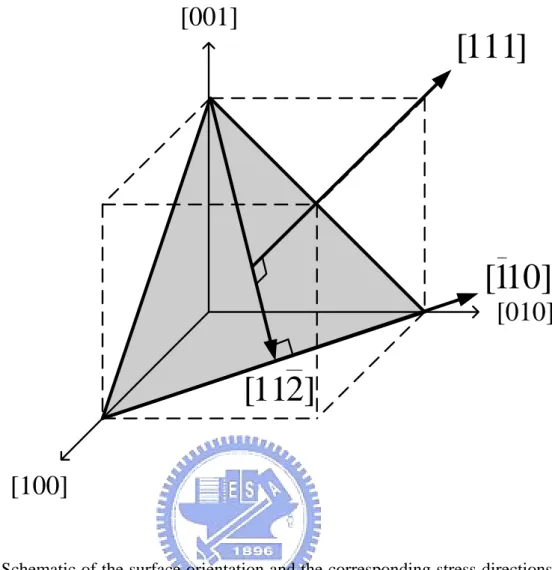
...64 Fig. 2.3. Schematic of the surface orientation and the corresponding stress directions
for (001) wafer. The shadow region indicates the wafer surface. The surface normal is [001], the longitudinal (channel) direction is [110], and the transverse direction, which is perpendicular to the channel in the plane, is [110]. ...65 Fig. 2.4. Schematic of the surface orientation and the corresponding stress directions
for (110) wafer. The shadow region indicates the wafer surface. The surface normal is [110], the longitudinal (channel) direction is [110], and the transverse direction, which is perpendicular to the channel in the plane, is [001]. ...66 Fig. 2.5. Schematic of the surface orientation and the corresponding stress directions
for (111) wafer. The shadow region indicates the wafer surface. The surface normal is [111], the longitudinal (channel) direction is [110], and the transverse direction, which is perpendicular to the channel in the plane, is [11 2 ]. ...67 Fig. 2.6. Silicon valence band structures for (a) unstressed, (b) 1GPa uniaxial
longitudinal compressive, (c) 1GPa uniaxial longitudinal tensile, (d) 1GPa uniaxial transverse compressive, and (e) 1GPa uniaxial transverse tensile stress on (001) wafer. ...68 Fig. 2.7. Silicon valence band structures for (a) 1GPa biaxial compressive and (b)
1GPa biaxial tensile stress on (001) wafer. ...69 Fig. 2.8. Silicon valence band structures for (a) unstressed, (b) 1GPa uniaxial
longitudinal compressive, (c) 1GPa uniaxial longitudinal tensile, (d) 1GPa uniaxial transverse compressive, and (e) 1GPa uniaxial transverse tensile stress on (110) wafer...70 Fig. 2.9. Silicon valence band structures for (a) unstressed, (b) 1GPa uniaxial
longitudinal compressive, (c) 1GPa uniaxial longitudinal tensile, (d) 1GPa uniaxial transverse compressive, and (e) 1GPa uniaxial transverse tensile stress on (111) wafer...71 Fig. 2.10. Strain-induced hole subband energy shift versus (a) uniaxial longitudinal
and (b) uniaxial transverse stress on (001) wafer. ...72 Fig. 2.11. Strain-induced hole subband energy shift versus biaxial stress on (001)
wafer. ...73 Fig. 2.12. Comparison between the strain-induced hole subband energy shift
calculated by 4×4 and 6×6 Hamiltonian for (a) uniaxial longitudinal and (b) biaxial stress on (001) wafer. The solid line indicates the subband energy calculated by the 6×6 Hamiltonian. The dotted line indicates the subband
energy calculated by 4 by 4 Hamiltonian. ...74 Fig. 2.13. Strain-induced hole subband energy shift versus (a) uniaxial longitudinal
and (b) uniaxial transverse stress on (110) wafer. ...75 Fig. 2.14. Strain-induced subband energy shift versus (a) uniaxial longitudinal and (b) uniaxial transverse stress on (111) wafer...76 Fig. 2.15. Hole constant energy surface of unstressed bulk silicon for three lowest
bands...77 Fig. 2.16. Hole constant energy surface of silicon under 1GPa uniaxial longitudinal (a)
compressive and (b) tensile stress on (001) wafer for three lowest bands. .... ...78 Fig. 2.17. Hole constant energy surface of silicon under 1GPa uniaxial transverse (a)
compressive and (b) tensile stress on (001) wafer for three lowest bands. .... ...79 Fig. 2.18. Hole constant energy surface of Silicon under 1GPa biaxial (a) compressive and (b) tensile stress on (001) wafer for three lowest bands. ...80 Fig. 2.19. Hole constant energy surface of silicon under 1GPa uniaxial longitudinal (a)
compressive and (b) tensile stress on (110) wafer for three lowest bands. .... ...81 Fig. 2.20. Hole constant energy surface of silicon under 1GPa uniaxial transverse (a)
compressive and (b) tensile stress on (110) wafer for three lowest bands. .... ...82 Fig. 2.21. Hole constant energy surface of silicon under 1GPa uniaxial longitudinal (a)
compressive and (b) tensile stress on (111) wafer for three lowest bands. .... ...83 Fig. 2.22. Hole constant energy surface of silicon under 1GPa uniaxial longitudinal (a)
...84 Fig. 2.23. Contour map in kx, ky plane (kz=0) of unstressed bulk silicon on (001) wafer for three lowest valence bands. ...85 Fig. 2.24. Contour map in kx, ky plane (kz=0) of silicon under 1GPa uniaxial
longitudinal (a) compressive and (b) tensile stress on (001) wafer for three lowest valence bands. ...86 Fig. 2.25. Contour map in kx, ky plane (kz=0) of silicon under 1GPa uniaxial transverse (a) compressive and (b) tensile stress on (001) wafer for three lowest valence bands. ...87 Fig. 2.26. Contour map in kx, ky plane (kz=0) of silicon under 1GPa biaxial (a)
compressive (b) tensile stress on (001) wafer for three lowest valence bands. ...88 Fig. 2.27. Contour map in kx, ky plane (kz=0) of silicon under 1GPa uniaxial
longitudinal (a) compressive and (b) tensile stress on (110) wafer for three lowest valence bands. ...89 Fig. 2.28. Contour map in kx, ky plane (kz=0) of silicon under 1GPa uniaxial transverse (a) compressive and (b) tensile stress on (110) wafer for three lowest valence bands. ...90 Fig. 2.29. Contour map in kx, ky plane (kz=0) of silicon under 1GPa uniaxial
longitudinal (a) compressive and (b) tensile stress on (111) wafer for three lowest valence bands. ...91 Fig. 2.30. Contour map in kx, ky plane (kz=0) of silicon under 1GPa uniaxial transverse (a) compressive and (b) tensile stress on (111) wafer for three lowest valence bands. ...92 Fig. 2.31. Band structures, constant energy surface, and energy contour of bulk silicon
tensile stress on (a) (001) and (b) (110) wafer, respectively...93
Chapter 3
Fig. 3.1. Effective masses along the three axes of the ellipsoid, m[ ]110 , m[ ]110 , and , versus uniaxial longitudinal stress for three lowest valence bands. .... ...94
[ ]001
m
Fig. 3.2. 3D (bulk) and 2D DOS effective masses versus uniaxial longitudinal stress for three lowest valence bands. ...95 Fig. 3.3. Effective masses along the three axes of the ellipsoid, , , and
, versus biaxial stress for three lowest valence bands. ...96 [ ]100
m m[ ]010
[ ]001
m
Fig. 3.4. 3D (bulk) and 2D DOS effective masses versus biaxial stress for three lowest valence bands. ...97 Fig. 3.5. Schematic of the strain-induced energy valleys splitting for (a) conduction
band electrons and (b) valence band holes...98 Fig. 3.6. Conduction and valence effective DOS, Nc and Nv, versus uniaxial stress. ...
...99 Fig. 3.7. Conduction and valence effective DOS, Nc and Nv, versus biaxial stress...
... 100 Fig. 3.8. Fermi energy of bulk silicon versus uniaxial stress for various doping
concentrations. The figure also shows the intrinsic Fermi level, conduction band edge, and valence band edge versus stress. ... 101 Fig. 3.9. Fermi energy of bulk silicon versus biaxial stress for various doping
band edge, and valence band edge versus stress. ... 102 Fig. 3.10. Intrinsic carrier concentration versus uniaxial and biaxial stress... 103
Chapter 4
Fig. 4.1. Valence band hole dispersion relation along [100] and [110] direction for the three lowest bands calculated by six-band k‧p method under channel inversion condition (FSi=1MV/cm). The external stress is (a) unstressed and
(b) 500MPa uniaxial compressive stress along [110] direction. ... 104 Fig. 4.2. Schematic of band diagram of a p+ polysilicon/SiO2/n-Si structure biased in channel inversion condition and stressed with uniaxial longitudinal compressive stress. The solid lines indicate the conduction and valence band edge without external stress. The dotted lines indicate the stress induced band edge shift of the conduction and valence band. The figure also shows the energy quantization effect in the channel inversion layer and hole direct tunneling current from the channel inversion layer to the polysilicon gate under stress. ... 105 Fig. 4.3. Schematic of the band diagram of a p+ polysilicon/SiO2/n-Si (pMOS)
structure, which is biased a negative gate voltage. The poly gate and channel are under arbitrary strain. The expression of flat band voltage for pMOSFETs under arbitrary strain can be derived with the help of this diagram... 106 Fig. 4.4. Schematic of band diagram of an n+ polysilicon/SiO2/p-Si structure biased in channel inversion condition and stressed with uniaxial longitudinal compressive stress. The solid lines indicate the conduction and valence band edge without external stress. The dotted lines indicate the stress induced
band edge shift of the conduction and valence band. The figure also shows the energy quantization effect in the channel inversion layer and electron direct tunneling current from the channel inversion layer to the polysilicon gate under stress. ... 107 Fig. 4.5. Schematic of the band diagram of an n+ polysilicon/SiO2/p-Si (nMOS)
structure, which is biased a positive gate voltage. The poly gate and channel are under arbitrary strain. The expression of flat band voltage for nMOSFETs under arbitrary strain can be derived with the help of this diagram... 108 Fig. 4.6. Hole subband energy at gamma point versus FSi without external stress. The
circles are data calculated by the six-band k ‧ p method with Schrödinger-Poisson equation. The solid lines are the fitting by the triangular potential approximation and the improved one band EMA. The figure also shows the quantization effective mass of the three lowest bands for best fitting. ... 109 Fig. 4.7. Hole subband energy at gamma point versus stress with various FSi. (a) First
band, (b) second band, and (c) third band. The circles are data calculated by k dot p method with Schrödinger-Poisson equation. The solid lines are the data calculated by Equation (4.1) for the three lowest bands, respectively....
... 110 Fig. 4.8. The strain-induced band edge shift versus stress for bulk silicon (a)
conduction and (b) valence band... 111 Fig. 4.9. (a) ΔJHDT/JHDT versus Stress. The squares, diamonds, and circles are data
published by former works. The solid lines are the simulation result by our model. (b) Hole subband energy versus stress. (c) Carriers density versus stress. (d) Hole direct tunneling current density versus stress. ... 112
Fig. 4.10. (a) ΔJEDT/JEDT versus Stress. The squares, diamonds, and circles are data
published by former works. The solid lines are the simulation result by our model. (b) Electron subband energy versus stress. (c) Carriers density versus stress. (d) Electron direct tunneling current density versus stress... 113 Fig. 4.11. Compare the influences of electron direct tunneling current between the two different doping concentrations of substrate. ... 114
Chapter 1
Introduction
In advanced nanotechnology, strain process has been extensively used for enhancing device performance [1], [2]. Therefore, having fundamental understanding of strain physics and studying the influences of strain in the nano-scale Si devices are essential. Moreover, developing a physically reasonable model and incorporating it into a quantum simulator in order to provide clear insight for future strain engineering and assess the influences of strain, such as subband energy splitting, repopulation of carrier density in each subband, and change of gate direct tunneling current, is crucial as well.
In order to give insights into the future strained devices while meeting the high performance and low power requirements, we first examine several potential stress types on various wafer orientations in Chapter 2. The simulation results including the strain-altered band structure, strain-induced band edge shift, constant energy surface in momentum space, two-dimensional energy contour, and the effective masses along the different crystallization directions, which are calculated by the deformation potential theory for conduction band and k‧p framework for valence band, are utilized to be the tools for estimating device performance. In addition, the influences of additional transverse stress, which is existent in process such as capping layer or STI stressor when the dimension of channel width is comparable with channel length, but usually ignored in former work, are addressed as well.
Second, in order to understand the properties of bulk silicon such as the Fermi level and intrinsic carrier concentration in the presence of strain, we utilize the
strain-altered band structures and the effective mass approximation to calculate the quantization effective mass, 2D DOS effective mass, and 3D DOS effective mass of bulk silicon under uniaxial and biaxial stress on (001) wafer in Chapter 3. Consequently, the effective DOS, Fermi energy, and intrinsic carrier concentration are also extracted with stress varying from zero to 3GPa. However, it is noticeable that the effective mass approximation, or the hypothetical elliptic constant energy surface, is suitable for large strain due to the strain symmetry, but introduces large error under small strain.
Third, in IC industry, the phenomenon of gate direct tunneling current in MOSFETs induces many problems such as standby power consumption, leakage current in C-V measurement, and etc. [3]-[5]. In the recent years, the dimension of device keeps scaling down while gate oxide thickness keeps thinning. Even the thickness is only several atomic layers. Therefore, the drawback of gate direct tunneling current becomes severe and influences the normal operation of devices [3]. On the other hand, in the advanced nanotechnology, the strain process is extensively used. Selecting the type of strain appropriately may enhance the mobility and alleviate the gate leakage in the meantime [1], [2], [6]. Thus, a computing efficient and reasonably physical model for characterizing and modeling the gate direct tunneling current of strained silicon device is essential. In chapter 4, we have developed a triangular potential approximation based quantum simulator for strained MOSFETs modeling.
Chapter 2
Strain-altered Band Structures
2.1 Introduction
In this chapter, we first review the topic of mechanics of materials and the equilibrium analysis of deformable bodies. Next, the well recognized methods, namely the deformation potential theory for conduction band and k‧p framework for valence band, are introduced to calculate the strain-altered band structure (energy dispersion relation). Then, in order to give insights into the future strained devices while meeting the high performance and low power requirements, several potential wafer orientations, (001), (110), and (111), with various stress conditions including uniaxial longitudinal, uniaxial transverse, and biaxial stress, will be examined. The calculated results in terms of the band structures, effective masses, strain-induced subband energy shift, constant energy surface, and two-dimensional energy contour, will exhibit the ability to quantitatively determine the device performance. Finally, the influences of the additional transverse strain on the devices will also been discussed.
2.2 A Review of Mechanics of Materials
In this section, we first review the concept of stress and strain, and then make a connection between the two. Note that the stress and strain produced by the change of temperature [7] are not included, that is, the temperature remains constant in this work.
2.2.1 Stress
intensity of stress is expressed as force per unit area [7], [8]. There are two types of stress: normal stress and shear stress. To illustrate this, let us consider an arbitrary force vector ΔR
( )
P at certain point P acting on an infinitesimal area Δ with Anormal vector n as shown in Fig. 2.1(a). The force is resolved into normal and tangential components ΔF
( )
P and ΔV( )
P . The tangential component is further resolved into components along two orthogonal directions, s and t in the plane. Then, the normal stress σn and the shear stress τns and τnt at point P are defined by the following expressions [7]:( )
( )
⎟ ⎠ ⎞ ⎜ ⎝ ⎛ Δ Δ = → Δ A P F P A nlim
0 σ (2.1a)( )
( )
⎟ ⎠ ⎞ ⎜ ⎝ ⎛ Δ Δ = → Δ A P V P s A nslim
0 τ (2.1b)( )
( )
⎟ ⎠ ⎞ ⎜ ⎝ ⎛ Δ Δ = → Δ A P V P t A ntlim
0 τ . (2.1c)Next, we expand above definitions of stress on a particular plane to all three mutually orthogonal planes that intercept a given common point in a deformable body as shown in Fig. 1(b). In the figure, σii refers to the normal stress components acting on the planes perpendicular to i-direction, while τ indicates the shear stress ij components oriented in the j-direction acting on the planes perpendicular to i-direction. According to Cauchy’s equation of motion, these nine components are sufficient to define the stress state at any point in a deformable body [8]. Furthermore, at moment equilibrium, the shear stress components must satisfy τij =τji [7]. Thus, a stress tensor with six independent components is sufficient to describe the state of stress:
⎥ ⎥ ⎥ ⎥ ⎥ ⎥ ⎥ ⎥ ⎦ ⎤ ⎢ ⎢ ⎢ ⎢ ⎢ ⎢ ⎢ ⎢ ⎣ ⎡ = xy zx yz zz yy xx τ τ τ σ σ σ σ . (2.2) 2.2.2 Strain
When a deformable body is subjected to external forces, it changes size and/or shape in response to the applied forces. The deformation of the body may include both changes of length (normal strain) and changes of angles (shear strain). For example, let us first focus on the case of a normal stress applied to the deformable body along the y-axis as shown in Fig. 2.2(a). A positive value for the stress σ , that y is, a tensile stress, causes the body to elongate along y-axis and to contract along x and z-axis. On the other hand, a negative value for the stress σ indicates y compressive stress, hence causing the body to be shortened along y-axis and dilated along x and z-axis. The normal strain is defined as
L L L L L = − Δ = ' ε (2.3)
where L, L’, and LΔ denote the original length, the length after deformation has occurred, and the total elongation of the body along y-axis, respectively. A positive value for strain ε indicates the body is stretched along y-axis, that is, L’ > L, and is called tensile strain. A negative value for ε indicates that the body is contracted along y-axis, that is, L’ < L, and is referred to as the compressive strain.
Next, let us consider that a body deforms due to the pure shear stress as shown in Fig. 2.2(b). After deformation, the original right angle π/2 becomes an acute angle θ′. The shear strain is defined as the change in angle between two originally perpendicular line segments as shown in Fig. 2.2(b). Thus, we have [7], [9], and [10]
y u z uy z zy yz ∂ ∂ + ∂ ∂ = ′ − = =γ π θ γ 2 . (2.4)
Likewise, we extend these definitions of normal strain and shear strain to the three mutually orthogonal planes [8]-[10]
x ux xx ∂ ∂ = ε , y uy yy ∂ ∂ = ε , z uz zz ∂ ∂ = ε (2.5a) x u y ux y yx xy ∂ ∂ + ∂ ∂ = =γ γ (2.5b) y u z uy z zy yz ∂ ∂ + ∂ ∂ = =γ γ (2.5c) x u z ux z xz zx ∂ ∂ + ∂ ∂ = =γ γ (2.5d)
where ux, uy, and uz are the displacements in the x, y, and z direction, respectively. It is
worth noting that γ denotes engineered shear strain and ij ε is called average shear ij strain and defined as one half the γ [9], [10]. ij
Similar to stress tensor, the strain tensor is also composed of six independent components ⎥ ⎥ ⎥ ⎥ ⎥ ⎥ ⎥ ⎥ ⎦ ⎤ ⎢ ⎢ ⎢ ⎢ ⎢ ⎢ ⎢ ⎢ ⎣ ⎡ = xy zx yz zz yy xx ε ε ε ε ε ε ε . (2.6)
2.2.3 Relationship between Stress and Strain
When a small normal stress, which remains well below the yield point, is applied to a homogeneous and isotropic body, the linear relationship between normal stress and normal strain can be described by Hooke’s law [7],
ε
σ =E (2.7)
associated with the normal strain of an elastic body in the direction of the applied normal stress, there is usually a transverse strain in two other directions, as illustrated in Fig. 2.2(a). The relationship between normal strain and transverse strain is described by [7], [9]
long tran νε
ε =− (2.8)
where the constant of proportionality v represents the Poisson’s ratio. Finally, to relate shear stress and shear strain, the Hooke’s law for shear is used [7], [9]
γ
τ =G (2.9)
where the constant of proportionality G represents the shear modulus of elasticity. By the principle of linear superposition, we can use the equations (2.7), (2.8), and (2.9) to combine strain response by adding together the separate responses produced by the six components of stress tensor. Consequently, the generalized Hooke’s law for isotropic materials is expressed as [7]
(
)
[
xx yy zz]
xx v E σ σ σ ε = 1 − + (2.10a)(
)
[
yy xx zz]
yy v E σ σ σ ε = 1 − + (2.10b)(
)
[
zz xx yy]
zz v E σ σ σ ε = 1 − + (2.10c) xy xy Gτ γ = 1 , xz xz Gτ γ = 1 , yz yz Gτ γ = 1 . (2.10d)It is noteworthy that for isotropic materials, shear strains are independent of normal stresses, and, likewise, normal strains are independent of shear stresses. In addition, the three components of shear are uncoupled [7].
For convenience, we usually combine the equations (2.2), (2.6), and (2.10) to establish the elastic strain-stress matrix for relating stress tensor and strain tensor [8], [10]-[12].
⎥ ⎥ ⎥ ⎥ ⎥ ⎥ ⎥ ⎥ ⎦ ⎤ ⎢ ⎢ ⎢ ⎢ ⎢ ⎢ ⎢ ⎢ ⎣ ⎡ ⎥ ⎥ ⎥ ⎥ ⎥ ⎥ ⎥ ⎥ ⎦ ⎤ ⎢ ⎢ ⎢ ⎢ ⎢ ⎢ ⎢ ⎢ ⎣ ⎡ = ⎥ ⎥ ⎥ ⎥ ⎥ ⎥ ⎥ ⎥ ⎦ ⎤ ⎢ ⎢ ⎢ ⎢ ⎢ ⎢ ⎢ ⎢ ⎣ ⎡ xy zz yz zz yy xx xy zx yz zz yy xx S S S S S S S S S S S S τ τ τ σ σ σ ε ε ε ε ε ε 44 44 44 11 12 12 12 11 12 12 12 11 0 0 0 0 0 0 0 0 0 0 0 0 0 0 0 0 0 0 0 0 0 0 0 0 2 2 2 (2.11)
where S11, S12, and S44 are the elastic stiffness constants.
These relationships can be determined experimentally by performing certain stress-strain and torsion tests [7]. Some extracted values of bulk Silicon for Young’s modules (130GPa for <100> directions and 169GPa for <110> directions), Poisson’s ratio (0.22-0.28), and shear modulus (79.9GPa) can be found in [8], [13]-[16]. Then, using these values, the elastic stiffness constants, S11, S12, and S44 can be evaluated.
The values used in this work are listed in Table 2.1. Note that although silicon is an anisotropic crystal, for the purposes of simplification it is conventional to use the equation (2.11) for mechanical analysis of bulk silicon [8], [11], and [12].
2.3 Hamiltonian
The deformation potential theory [17] (for conduction band) and k‧p Framework [18], [19] (for valence band) are the primary [18] method to calculate the strain-altered band structures including band shift and warping to date.
2.3.1 Hamiltonian for Conduction Band (Deformation Potential Theory)
In deformation potential theory, the total Hamiltonian for each energy valleys of silicon conduction band is [18]
(
)
(
l u ij d c t t l l Tr E m k m k k H ⎟⎟+ +Ξ ε +Ξ ε ⎠ ⎞ ⎜⎜ ⎝ ⎛ + − = ( ) 2 2 * 2 2 * 2 0 2 h h)
(2.12)perpendicular to the <100> directions of each energy valleys, respectively. and are the longitudinal and transverse effective mass, respectively. Ec is the conduction band edge of untrained bulk silicon.
* l m * t m d
Ξ and Ξ are the dilation and u uniaxial deformation potential for silicon conduction band, respectively. Tr(ε ij)
stands for the trace of the strain tensor. εl is the longitudinal strain component. Note that and are generally assumed to be constant since they do not change significantly under small or moderate strain [12], [18]. In other words, the strains do not alter the energy dispersion in conduction band, the first part of Equation (2.12), but just shift the band edge, the second part. Appling Equation (2.12), the quantities of band edge shift for the six conduction band minima along the <100> directions can be expressed as [12] * l m mt*
(
xx yy zz)
u xx d C E =Ξ ε +ε +ε +Ξ εΔ for the valleys along [100] and [100] (2.13a)
(
xx yy zz)
u yy dC
E =Ξ ε +ε +ε +Ξ ε
Δ for the valleys along [010] and [010] (2.13b)
(
xx yy zz)
u zz dC
E =Ξ ε +ε +ε +Ξ ε
Δ for the valleys along [001] and [001] (2.13c)
Note that the shear strain terms do not contribute to the band shift, and the strain-induced band edge shift is only proportional to the normal strain terms.
2.3.2 Hamiltonian for Valence Band (k‧p Framework)
The influences of strain on valence band structures include not only band shifts, but also strong band warping. Thus, the deformation potential theory, which considers only the band shift, cannot serve for valence band. In order to calculate the strain-altered valence band structures of bulk silicon, we employ the six-band k‧p method [20]. The k‧p method is based on perturbation theory and symmetry
consideration [18]. The strain effects can be easily introduced to k‧p framework [18], [21]. According to Pikus and Bir [18], the strain Hamiltonian is formally identical to the k‧p Hamiltonian (Luttinger Hamiltonian) [18]. The correspondence between the strain and k‧p Hamiltonian is kikj ↔εij and the total Hamiltonian is given by
[18]. The total Hamiltonian is expressed by [18], [21]
strain p k H H H = ⋅ + ⎥ ⎥ ⎥ ⎥ ⎥ ⎥ ⎥ ⎥ ⎥ ⎥ ⎥ ⎥ ⎥ ⎥ ⎥ ⎦ ⎤ ⎢ ⎢ ⎢ ⎢ ⎢ ⎢ ⎢ ⎢ ⎢ ⎢ ⎢ ⎢ ⎢ ⎢ ⎢ ⎣ ⎡ Δ − − − − − Δ − − − − − − − − − − + − − − − + − − − − − = + = + + + + + + + + + + + + ⋅ P L Q L M P M L Q L L M Q P L M Q L L Q P M L Q M Q P L M L M L Q P H H H kp strain 0 2 1 2 2 3 2 0 2 2 3 2 2 1 2 1 2 0 2 2 3 0 2 3 2 0 2 2 1 0 (2.14) where P=Pk+Pε, Q=Qk+Qε, L=Lk+Lε, and M =Mk+Mε. The symbol Δ is the split-off energy. The k‧p terms in the Hamiltonian are defined as
(
2 2 2 1 0 2 2 x y z k k k k m P = h γ + +)
(2.15a)(
2 2 2 2 0 2 2 2 x y z k k k k m Q = h γ + −)
(2.15b)(
x y z k k ik k m L = 3 − 0 2 3γ h)
(2.15c)(
)
[
x y x y k k k i k k m M 2 2 2 3 0 2 2 3 2 γ − − γ − = h]
(2.15d)where γ , 1 γ , and 2 γ3 are the Luttinger parameters. is the mass of free electron.
k
0
m
x, ky, and kz are the wavevectors along x, y, and z-axis, respectively. The strain terms
in the Hamiltonian are defined as
(
xx yy zz)
v a Pε =− ε +ε +ε (2.16a)(
xx yy zz)
b Qε ε ε 2ε 2 + − − = (2.16b)(
xz i yz)
d Lε =− ε − ε (2.16c)(
xx yy)
id xy b Mε = ε −ε − ε 2 3 (2.16d) where a, b, and d are the deformation potentials for valence band. The components of strain tensor are defined in Equation (2.5) and (2.6). The values of the Luttinger parameters and deformation potentials for silicon are given in Table 1. Note that the valence band edge for unstrained silicon is at zero value in this expression.For the sake of brevity, many works ignored the coupling effect of the split-off band. In this case, the Hamiltonian of the top and second band can be described by a 4×4 Hamiltonian [the upper-left 4×4 matrix block in Equation (2.14)].
⎥ ⎥ ⎥ ⎥ ⎦ ⎤ ⎢ ⎢ ⎢ ⎢ ⎣ ⎡ − − − − − + − − − + − − − − = + + + + Q P L M L Q P M M Q P L M L Q P H 0 0 0 0 (2.17)
Then, the analytic solution of the valence band structure for top two bands can be obtained as 2 2 2 ) (k P Pε Q Qε L Lε M Mε E =− k− ± k + + k + + k+ (2.18)
In section 2.4.2, we will discuss the differences in the strain-induced subband energy shift calculated by the 6×6 and 4×4 Hamiltonian.
The valence bands for all diamond and zinc blende structure semiconductors whose band gap is much larger than the split-off energy can be calculated using the Luttinger Hamiltonian. Thus, using the corresponding parameters, the deformation potentials, Luttinger parameters, elastic stiffness constants, and split-off energy, as listed in Table 2.1, the band structures for the other two typical semiconductors, Ge and GaAs, can be evaluated as well.
2.4 Types of Stress and
Various Wafer Orientations
In this section, we first define the directions of normal, longitudinal, and transverse stress for three conventional wafer orientations, (001), (110), and (111). Then, the stress tensors and strain tensors for these wafer orientations are expressed as a function of the corresponding normal, longitudinal, and transverse stress.
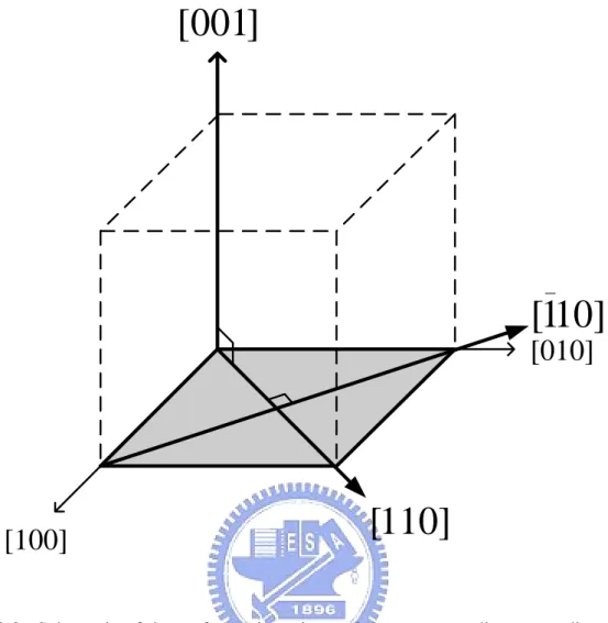
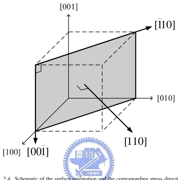
Fig. 2.3, 2.4, and 2.5 show the surface orientations and the corresponding stress directions for (001), (110), and (111) wafer, respectively. The shadow region indicates the wafer surface. For (001) wafer, the surface normal or out-of-plane direction is along [001], the longitudinal (channel) direction is along [110], and the transverse direction, which is perpendicular to the channel in the plane, is along [110]. The biaxial stress for (001) wafer is along [100] and [010] directions with the same magnitude of stress, that is, σ[ ]100 =σ[ ]010 . For (110) wafer, the surface normal direction is along [110]. The [110] direction is chosen as the channel direction for higher hole mobility in the plane [19]. The transverse direction is along [001]. For (111) wafer, the surface normal is along [111], the longitudinal direction is along [110], and the transverse direction is along [11 2 ]. The stress directions for the three wafer orientations are also summarized in Table 2.2. Note that (110) and (111) wafers have no so-called biaxial stress since the longitudinal and transverse direction are not
symmetric in silicon crystal.
In addition, the channel directions are indeed the same on (001), (110), and (111) wafer since the [110] and [110] have the same symmetry in silicon crystal; however, the normal and transverse directions are different. Thus, if additional normal or transverse stresses exist in devices, it would induce different band structures among these wafer orientations.
Using the discussion in Section 2.1, the stress tensors and strain tensors for biaxial stress on (001) wafer, uniaxial stress along [110], [110], [001], [111], and [11 2 ] direction can be obtained and listed in Table 2.3. By the principle of linear superposition, the resultant strain tensor in response to the combination of normal, longitudinal, and transverse stress for the three wafer orientations are also obtained and given in Table 2.4. Note that although the normal, longitudinal, and transverse stresses on (001) and (110) wafer are along different directions, they are indeed among the same set of stress directions, that is, [110], [110], and [001]. That implies the same strain-altered band structures can be achieved on (001) and (110) wafer with the corresponding stresses included.
2.5 Results and Discussion
2.5.1 Band Structures
Applying Table 2.4 and Equations (2.12)-(2.16), the calculations of strain-altered band structures on the three wafer orientations with various stress conditions are straightforward.
As discussed before, the band warping of silicon conduction band remains unchanged (band edge shift will be discussed in next section). The valence band structures with various strain conditions including unstressed bulk silicon, 1GPa
uniaxial longitudinal compression, 1GPa uniaxial longitudinal tension, 1GPa uniaxial transverse compression, and 1GPa uniaxial transverse tension, are shown in Fig. 2.6, 2.8, and 2.9 for (001), (110), and (111) wafer, respectively. Fig. 2.7 also shows the 1GPa biaxial compressive and tensile stress on (001) wafer. The right hand side of the figures is along the out-of-plane direction, and the left hand counterpart is along the channel direction. Moreover, the band structures are plotted in electron energy, that is, more positive value at energy axis represents smaller hole energy. The effective masses along normal and channel direction for the three lowest bands are also marked in the figures. The three lowest valence bands in Fig. 2.6-2.9 are denoted as top, second, and third band since the designations, heavy, light, and split-off, lose their meanings under stress. For example, Fig. 2.6(b) shows the band structure of bulk silicon under uniaxial compressive stress on (001) wafer. The top band along [001] direction is “heavy-hole like” and second band is “light-hole like,” but along [110] direction, the situation is reverse: the top band becomes “light-hole like” and second band is “heavy-hole like.”
2.5.2 Strain-induced Band Edge Shift
In order to give insight into the trends of strain-altered band structures from small to large strain, there are two characteristics of band structures that should be considered. One is band edge shift discussed in this section, and the other is band warping which will be modeled into effective masses and extracted in Chapter 3.
Using Equation (2.12) and Table 2.4, the band edge shift of the six conduction band minima along the <100> directions can be obtained. Note that the first term of Equation (2.13) shifts the six valleys in the same magnitude while the second term splits the Δ4 valleys (the conduction band minima along [100], [100], [010], and [010] directions) and Δ2 valleys (the minima along [001] and [001] directions) since
zz yy xx ε ε
ε = ≠ for all stress types in the discussion. Also note that associated with compressive (tensile) strain in one direction, there are generally a tensile (compressive) strain in the other two directions. Thus, the signs of εxx (ε ) and yy ε are opposite zz for a single uniaxial or biaxial stress. On the other hand, with the combination of the normal, longitudinal, and transverse stress, the εxx (ε ) and yy ε may be produced zz
with the same sign. However, it indeed favors opposing sign for increasing the population in the lowest subband and enhancing mobility.
Using Table 2.4 and Equation (2.14)-(2.16) with kx =ky =kz =0 , the
strain-induced valence subband energy shift can be obtained since the valance band minima for bulk silicon are all at gamma point (see Fig. 2.6-2.9). The three lowest valence band edges versus stress with uniaxial longitudinal, uniaxial transverse stress are shown in Fig. 2.10, 2.13, and 2.14 for (001), (110), and (111) wafer, respectively. Fig. 2.11 also shows the biaxial stress case on (001) wafer. The negative value of stress indicates compressive stress and the positive value indicates tensile stress. Note that the band edge shift under uniaxial longitudinal stress on (001), (110), and (111) wafer, and uniaxial transverse stress on (001) wafer are the same since these stress directions have the same symmetry in silicon crystal.
The figures also label the quantization effective mass, which is along the direction normal to the surface, for top two bands. The “hh” denotes the effective mass of the corresponding band as “heavy-hole like” while “lh” is “light-hole like” among the two bands. It is interesting that no matter whether the stress is uniaxial longitudinal, uniaxial transverse, or biaxial on the (001) wafer, under the compressive stress the first band is heavy-hole like and the second band is light-hole like. Nevertheless, under tensile stress, the situation is reverse. This is the main mechanism
accounting for the reverse trends of the change of direct tunneling current between compressive and tensile stress. It will be discussed thoroughly in Chapter 5. The analysis can be applied to (110) and (111) wafer as well.
Moreover, the subband energy splitting between top and second band is larger under uniaxial compression (biaxial tension) than uniaxial tension (biaxial compression). The influences will be discussed in chapter 3, 4, and 5.
Next, let us compare the difference between results calculated by the 6 6 Hamiltonian and the 4×4 Hamiltonian. The latter is widely used in the previous works for device modeling [16], [22] since its solutions have very simple form for biaxial stress on (001) wafer [Equation (2.19)] and uniaxial stress along [110] [Equation (2.20)]. The solutions can be obtained through Equation (2.18) and Table 2.4. Note that the band edge is proportional to the stress.
×
(
k) (
a S S) (
σ S S)
bσ Ev =0 = 2 11+4 12 ± 11 − 12 (2.19)(
) (
)
σ(
)
σ 2 1 2 44 2 2 12 11 2 12 11 16 4 2 0 ⎥ ⎦ ⎤ ⎢ ⎣ ⎡ + − ± + = = a S S b S S d S k Ev (2.20)On the other hand, the analytic solution of 6×6 Hamiltonian is complex for uniaxial stress along [110] and not listed here due to space limit. However, the solution of that for biaxial stress [Equation (2.21)] is relatively simple since biaxial stress have no shear strain terms and withεxx =εyy, thus, Lε =Mε =0 in Equation (2.14).
(
)
[
2 2]
12 9 2 2 1 2 1 2 1 0 Pε Qε or Pε Qε Qε Qε k Ev = =− − − − Δ+ ± Δ + Δ+ (2.21)Fig. 2.12 shows the comparison between the band edge shift calculated by 6×6 (solid line) and 4×4 (dotted line) Hamiltonian under uniaxial and biaxial stress on (001) wafer. It can be seen that under uniaxial or biaxial stress, one of the top two bands can be approximated by a straight line, hence the use of Equations (2.19) and
(2.20) can get fairly good results. However, the other band is far from the linear line calculated by 4×4 Hamiltonian and even the lowest energy is not located at zero stress, that is, it first decreases and then increases while the stress increases. Therefore, the usage of analytic solutions derived from 4×4 Hamiltonian can only serve for very small stress and induces significant error under moderate and large stress as shown in Fig. 2.12. For this reason, we will apply the 6× 6 Hamiltonian throughout our simulation work in Chapter 2, 3, and 4.
2.5.3 Constant Energy Surface
Constant energy surface in k-space is also an important tool for estimating the influences of strain and can be obtained from Equation (2.12) for conduction band and (2.14) for valence band. Fig. 2.16, 2.17, and 2.18 show the constant energy surface in k-space of bulk silicon for three lowest valence bands with 1GPa uniaxial longitudinal, uniaxial transverse, biaxial stress on (001) wafer, respectively. For comparison, Fig. 2.15 also shows the case of unstressed bulk silicon (the results are consistent with Ref. [23]). The three coordinate axes are along kx, ky, and kz. The figures also label the
effective masses along normal, longitudinal, transverse, and other principal directions. In addition, constant energy surface for bulk silicon under 1GPa uniaxial longitudinal and uniaxial transverse on (110) and (111) are shown in Fig. 2.19-2.22. Note that, in these figures, the three coordinate axes are along the normal, longitudinal, and transverse directions.
2.5.4 Two-dimensional Energy Contour in the Plane of Wafer Surface
The two-dimensional energy contour in the plane of wafer surface can help us determine the characteristics of inversion layer of MOSFETs including the conductivity effective mass, transverse effective mass, density of states, and the
symmetry of E-k relation under various stress conditions.
The energy contour of valence band can be obtained by Equation (2.14) and setting the wavevector along normal direction at zero. The results are plotted in Fig. 2.23-2.30 for various stress conditions and wafer orientations as discussed above. Note that the horizontal and vertical axes are along kx and ky for (001) wafer and,
contrary to that, they are along the longitudinal and transverse directions for (110) and (111) wafers.
2.5.5 Advantageous Strains and Wafer Orientations
The general expression of conductivity for n- or p-MOSFETs operating in inversion condition can be described by
⎥ ⎦ ⎤ ⎢ ⎣ ⎡ ⎟⎟ ⎠ ⎞ ⎜⎜ ⎝ ⎛ + ⎟⎟ ⎠ ⎞ ⎜⎜ ⎝ ⎛ = 2 2 2 1 1 1 c c m q n m q n q ty Conductivi τ τ (2.22) where q, n, τ , and mc are the elementary charge, carrier density, scattering relaxation
time, and conductivity effective mass along channel direction, respectively. The subscript denotes the first and second subband in the inversion layer of MOSFETs.
For high performance and low power requirements, advantageous strains need to meet following criteria [2], [24]-[26]: (1) small conductivity effective mass of the lowest subband, mc1, for enhancing the mobility since most of carriers occupy the
lowest subband; (2) large quantization effective mass along the out-of-plane direction of the lowest subband, which enhances the carrier population by lowering the quantization energy in the inversion layer; (3) large 2D DOS effective mass, or large transverse effective mass, of the lowest subband which also increases the carrier population of the lowest subband; (4) large energy splitting of the two lowest subbands for lowering the intervalley (optical phonon) scattering; and (5) the strain-induced subband shift and confinement effect in inversion layer are additive,
that is, the band shifted down by strain must also have a larger quantization effective mass, whereas the band shifted up by strain must have a smaller quantization effective mass. The requirement not only enhances mobility due to increased carrier population in lowest subband which have small conductivity effective mass, but also reduces the power dissipation due to decreased gate direct tunneling current (details will be discussed in Chapter 4).
Let us first examine the potential stress types and wafer orientations with these criteria for nMOSFETs, then, for pMOSFETs. The quantization, conductivity, and DOS effective masses of the lowest subbands for nMOSFETs operating in inversion conditions are given by [27]-[29] and listed in Table. 2.5. For conservative reason, we assume the stress is not large enough to perturb significantly the original system described in [27]-[29]. Under this assumption, the effective masses keep constant under strain, that is, strain has no influences on the criteria 1-3. In addition, the total carrier density in inversion layer does not change significantly when the carriers repopulate from one subband to another subband due to the strain-induce subband energy shift.
For criterion 5, uniaxial longitudinal, uniaxial transverse, and biaxial tension are advantageous strains for (001) wafer since these strains lift the Δ4 valleys, which have smaller quantization effective mass, and shift down the Δ2 valleys, which have larger quantization effective mass [see Equation (2.13) and Table 2.4]. On the other hand, the uniaxial longitudinal compression are advantageous strains for (110) wafer since these strains lift the 2 valleys, which have smaller quantization effective mass, and shift down the 4 valleys, which have larger quantization effective mass. Note that the 4 valleys are the conduction band minima along [100], [
Δ Δ
Δ 100], [010], and
[010] directions while Δ2 valleys are the minima along [001] and [001] directions on both (001) and (110) wafer [27]. For the (111) wafer, the six valleys are degenerate
in inversion layer and have the same conductivity effective mass, that is, the strain-induced subband energy shift does not provide additional benefits for the conductivity.
For comparing the (001) and (110) wafer, let us consider the same carriers concentration in inversion layer on (001) and (110) wafer. The quantization effective mass of the lower valleys on (001) wafer is much larger than that of (110) wafer while for higher valleys, it remains the same. That is, the occupation ratio of the lower valleys is larger on (001) wafer than that on (110) wafer due to the much lower subband energy of lower valleys compared to higher valleys on (001) wafer. In addition, the conductivity effective mass of the lower valleys is smaller on (001) wafer than that on (110) wafer while for the higher valleys it is equivalent on both wafers. Moreover, the magnitudes of strain-induced subband energy shift are equivalent since the directions of uniaxial longitudinal stress on (001) and (110) wafers have the same crystal symmetry. Therefore, the conductivity on (001) wafer is better than that on (110) wafer. However, experiments and accurate numerical simulations must be conducted to corroborate this argument.
Next, let us examine these stress types and wafer orientations for pMOSFETs using the criteria, the simulation results, Fig. 2.6-2.30, and the effective masses summarized in Table 2.6. For criterion 5, the disadvantageous strains producing smaller quantization effective mass for top band and larger quantization effective mass for second band are marked with a strikethrough on the quantization effective mass. Then, for criteria 1-3, the advantageous strains producing smallest conductivity effective mass, largest transverse effective mass, and best quantization effective mass among these stress types and wafer orientations are emphasized with bold effective mass.
(001) and (110) wafers is better among all advantageous strains. For uniaxial longitudinal compression on (001) wafer, it can provide smallest conductivity effective mass and largest transverse effective mass of the top band, but the quantization effective masses are not as desirable as that on (110) wafer. On the other hand, uniaxial longitudinal compression on (110) wafer can provide the smallest conductivity effective mass as that on (100) wafer, the largest quantization effective mass of the top band, and the smallest quantization effective mass of the second band, which not only increases the carrier population in top band, but also reduces the gate direct tunneling current. However, the transverse effective masses are small comparing with that on (001) wafer. Moreover, the magnitudes of strain-induced band edge shift on both wafers are equivalent as shown in Fig. 2.10(a) and Fig. 2.13(a). Indeed, there are reported simulation results [26] indicating that the mobility on (110) wafer is larger than that on (001) wafer below about 1.3GPa, but the situation is reverse above 1.3GPa. Nevertheless, the conductivity and total drive current, which relate to the carrier density and occupation ratio of each subband, were not reported in the work. Therefore, there are advantages and disadvantages on each wafer orientation, but for low power application, (110) wafer may be better than (001) wafer.
2.5.6 Influences of Additional Transverse or Normal Stress
In Section 2.5.5, we concluded that uniaxial and biaxial tensile stresses on (001) wafer favor the conductivity enhancement for nMOSFETs while it is the uniaxial longitudinal compressive stress on both (001) and (110) wafer for pMOSFETs. Then, in this section, we focus on the influences on these advantageous stress with
additional uniaxial transverse stress, or normal stress, which is existent in process
such as capping layer or STI stressor when the dimension of channel width is comparable with channel length.
Let us first consider an additional transverse stress on (001) wafer, or an additional normal stress on (110) wafer with the same sign, that is, compressive stress, and magnitude of the longitudinal stress. It is possible in process such as capping layer or STI stressor. Table 2.4 shows that the shear strain term is canceled while the normal strain term is doubled. Thus, the strain tensors reduce to the form as biaxial compressive stress on (001) wafer (a pure normal stress). It is not desirable for pMOSFETs since the benefits of longitudinal compressive stress is degraded.
Next, let us consider additional transverse stress on (001) wafer, or normal stress on (110) wafer, with the opposing sign, that is, tensile stress, and the same magnitude of longitudinal stress. [Note that uniaxial longitudinal compressive and transverse tensile stresses are both advantageous strains on (001) wafer as shown in Fig. 2.6(e), Fig. 2.17(b), Fig. 2.25(b), and Table 2.6.] Table 2.4 shows that the normal strain terms are canceled while the shear strain term doubles. Thus, the strain tensors readily reduce to a pure shear strain. It is not desirable in nMOSFETs since there is no energy splitting between the 2 and 4 valleys due to the normal strain terms being zero. Thus, the mobility enhancement of nMOSFETs by uniaxial longitudinal stress is degraded. For pMOSFETs, Fig. 2.31 shows the band structures, constant energy surfaces, and 2D energy contours of bulk silicon with addition transverse stress on (001), and (110) and the effective masses are summarized in Table. 2.7. It can be found that with additional transverse tensile stress on (001) wafer, the conductivity effective mass remains 0.12m
Δ Δ
0 for top band, but that reduced from 0.59m0 to 0.3m0 for
second band. In addition, the transverse effective mass of top band increases from 1.37m0 to 1.88m0. Note that the simulated results for additional normal tensile stress
on (110) wafer are similar to that for an additional transverse tensile stress on (001) wafer, but the normal and transverse direction are exchanged. Thus, additional transverse tensile stress on (001) wafer can further enhance the hole mobility while
additional normal tensile stress on (110) wafer can further reduce the gate direct tunneling current (the quantization effective mass of top band increase from 1.37m0 to
1.88m0). On the other hand, additional transverse tensile stress have no apparent
benefits on (110) wafer as shown in Table 2.7.
To introduce the additional transverse tensile stress on (001) wafer for enhancing hole mobility, it is possible to be achieved without additional costs by modifying slightly the standard strained CMOS logic technology process flow [1]. The undertaken technology enhances the electron and hole mobility on the same wafer by first using SiGe source/drain to introduce longitudinal compressive stress in the channel of pMOSFETs and then introduces longitudinal tensile stress in the channel of nMOSFETs by applying nitride capping layer on both nMOSFETs and pMOSFETs. The disadvantage of this process flow is that it needs additional step for neutralizing the capping layer strain on pMOSFETs. However, instead of the longitudinal tensile stress with the nitride capping layer, if the tensile stress is incorporated along the transverse direction during the same step, which not only enhances the election mobility in the same order of magnitude, but also introduces additional hole mobility enhancement. (Remind that the longitudinal and transverse directions are symmetry in silicon crystal. Thus, the energy splitting of the Δ2 and Δ4 valleys are equivalent under these two type stresses. Moreover, effective masses remain unchanged in conduction band).
2.6 Conclusion
In this chapter, the strain tensors have been expressed as a function of normal, longitudinal, and transverse stress on (001), (110), and (111) wafers, respectively. Then, the strain-altered band structures, band edge shifts, constant energy surface, 2D energy contour, and effective masses for various stress conditions and wafer
orientations have been calculated by deformation potential theory and k‧p framework for conduction band and valence band, respectively. Utilizing these simulated results as tools to estimate the device performance, the best advantageous strains among these stress types and wafer orientations for nMOSFETs have shown to be uniaxial and biaxial tension on (001) wafer while for pMOSFETs they are uniaxial longitudinal compression on both (001) and (110) wafer. Finally, we have examined the influences of additional transverse or normal strain and have found that the additional transverse tensile stress on (001) wafer can further enhance the hole mobility.
Chapter 3
The Properties of Bulk Silicon in the Presence of
Strain
3.1 Introduction
In order to model the characteristics of strained MOSFETs such as the change of gate direct tunneling current (Chapter 4), there are two important features of strain-altered band structure that should be take into consideration. One is the strain-induced band edge shift, which has been discussed and extracted in Chapter 2. The other is the strain-induced band warping, which will be incorporated into our physical model (developed in Chapter 4) via the effective masses extracted in this chapter such as the quantization effective mass, the 2D density of state (DOS) effective mass, and 3D DOS effective mass. In Chapter 4, we will verify qualitatively and quantitatively that the strain-induced change of gate direct tunneling current can be attributed to these two features of strain-altered band structure. Moreover, utilizing the extracted 3D DOS effective masses and band edge shifts of all valleys, the conduction band effective DOS, Nc, and valence band effective DOS, Nv, can be
determined. Then, following the approach of conventional “Semiconductor Device Physics,” [30], [31] the strain-altered Fermi energy level of bulk silicon, which is an important physical parameter for device modeling, can be determined. Finally, the strain-altered intrinsic carrier density of bulk silicon will be calculated as well.
Note that in Chapter 3 and 4, it is primarily focused on the silicon under uniaxial longitudinal stress and biaxial stress on (001) wafer since there are adequate

![Table 2.3 The stress tensor and strain tensor for biaxial stress on (001) wafer, uniaxial stress along [110], [110], [001], [111], and [11 2 ] direction](https://thumb-ap.123doks.com/thumbv2/9libinfo/8410768.179836/77.892.126.770.188.491/table-stress-tensor-strain-tensor-biaxial-uniaxial-direction.webp)
![Table 2.5 Numerical values of effective mass for silicon conduction band in inversion layer given by [27]](https://thumb-ap.123doks.com/thumbv2/9libinfo/8410768.179836/79.892.130.768.188.360/table-numerical-values-effective-silicon-conduction-inversion-layer.webp)