國
立
交
通
大
學
電子工程學系 電子研究所碩士班
碩
士
論
文
射頻積體電路之基板雜訊耦合分析
及模型化
Analysis and Modeling of Substrate Noise Coupling in
RFICs
研 究 生:蔡坤宏
指導教授:郭建男 教授
射頻積體電路之基板雜訊耦合分析及模型化
Analysis and Modeling of Substrate Noise Coupling in
RFICs
研 究 生:蔡坤宏 Student:Kun-Hung Tsai
指導教授:郭建男
Advisor:Chien-Nan Kuo
國 立 交 通 大 學
電子工程學系 電子研究所碩士班
碩 士 論 文
A ThesisSubmitted to Department of Electronics Engineering & Institute of Electronics College of Electrical Engineering and Computer Science
National Chiao Tung University In Partial Fulfillment of the Requirements
For the Degree of Master
In
Electronic Engineering July 2005
Hsinchu, Taiwan, Republic of China
射頻積體電路之基板雜訊耦合分析及模型化
學生 : 蔡 坤 宏 指導教授 : 郭 建 男 教授
國立交通大學
電子工程學系 電子研究所碩士班
摘要
在本論文中,我們由頻域的觀點來探討射頻積體電路中,元件因
耗損性矽基板所產生的雜訊耦合效應。對此,論文分別針對射頻被動
元件(電感)及電晶體(MOSFET)所生的雜訊經由矽基板傳導的現象,
作分析及模型化。
被動元件部分,我們製作二種不同擺放方法的電感對,並改變其
距離,觀察電感所生的基板雜訊耦合效應對距離變化的情況,同時,
亦觀察電感受到雜訊耦合後,電感本身特性改變的情形。之後,再由
模擬及量測的相互驗證,提出雜訊耦合的等效電路模型,描述基板雜
訊的行為。
在電晶體部分,我們可以知道金氧半電晶體的源、汲二極因 P-N
接面的關係會產生寄生的空乏電容,此一寄生電容會將高頻的雜訊耦
合到基板,而使雜訊影響電路工作的準確性。針對此點,我們設計測
試鍵來量測高頻雜訊因接面電容耦合到基板的現象。在測試鍵中,我
們將
P-Well 及 N-Well 中分別打入 N-diffusion 及 P-diffusion 形成空乏
電容,同時調整
diffusion 的距離,並量測雙埠(Two-port)的散射參數
(S-parameter),得知高頻雜訊對距離變化的情況。
最後,這些量測結果及等效模型,將提供給電路設計者,期能經
由這些資訊,可讓高頻電路設計更有效率。
Analysis and Modeling of Substrate Noise Coupling in
RFICs
Student: Kun-Hung Tsai Advisor: Prof. Chien-Nan Kuo
Department of Electronics Engineering & Institute of Electronics
National Chiao.Tung University
ABSTRACT
In this thesis, the substrate noise coupling effect in the lossy silicon substrate is investigated from the aspect of frequency domain. Therefore, the coupling effect produced by the passive device and MOSFET is also analyzed and modeled.
In the part of passive device, two types of inductor pairs are fabricated and the distance between the inductor pairs is varied to observe the substrate coupling effect with regards to the different distance. Furthermore, the characteristic of inductor changed by coupling effect is also studied. Then, from the measurement and simulation results, an equivalent circuit model of substrate noise coupling effect in the inductor pairs is proposed, too.
In the part of MOS transistor, we study the noise coupling from the source and drain depletion capacitance (formed by the P-N junction). However, these parasitic capacitances would couple the RF noise to substrate and then degrade the performance of RF circuit. From the point of view, the testkey is designed to measure the phenomenon of RF noise coupling effect. In the testkey, the N-diffusion and P-diffusion regions are formed inside the P-well and N-well then induce the junction capacitance. Next, the distance of two diffusion regions is changed and measured the
S-parameters to obtain the noise coupling effect for the varying different distance. Finally, these measurement results and equivalent circuit model would provide to circuit designers and hope the information would let the RF circuit design procedure be more efficient.
誌謝
首先要感謝我的指導教授郭建男博士在這二年來給我的指導,老師豐富的學 識及治學嚴謹的態度,讓我在碩士班的修業過程中,獲益良多,在此向老師獻上 最深的敬意。 感謝一起在實驗室共患難的學長,同學及學弟妹們。同期的維嘉及仰鵑,在 我遇到困難時,不吝伸出援手,拉我一把,讓我在能順利的渡過。實驗室的大學 長,昶綜,更是在研究上時常提點我,讓我的研究能夠突破難關。同時,也要謝 謝凱哥在製程上的幫忙,以及子倫與NDL 的黃國威、邱佳松、卓銘祥先生在量 測上的協助,由於他們的鼎力相助,讓我有了畢業的機會,當然,達道與岱原也 為實驗室注入了活力,讓我在研究苦悶之餘,心情能夠獲抒解。 最後,還要感謝我的父母及鄒佩真小姐,他們是我心情的避風港,不管我遇 到了什麼問題,他們總是默默地支持我,給我鼓勵,讓我萌生勇氣,一步一步地 走完這段求學路。當然,也還有很多認識或不認識的朋友,給了我很多幫忙,在 此一併謝過。 蔡坤宏 九十四年七月CONTENTS
ABSTRACT (CHINESE) ... I
ABSTRACT (ENGLISH)... III
ACKNOWLEDGEMENT...V
CONTENTS... .VI
TABLE CAPTIONS... VIII
FIGURE CAPTIONS ... IX
CHAPTER 1 Introduction ...1
1.1 Motivation ... 1
1.2 Thesis organization ... 2
CHAPTER 2 Basic Concepts of the Coupling Effect
in Silicon Substrate ...3
2.1 Noise coupling in digital circuit ... 3
2.2 Electromagnetic coupling in Si substrate... 5
CHAPTER 3 Investigation of RF Spiral Inductor’s
Coupling Effects in Lossy Substrate ...7
3.1 Design consideration of a single inductor ... 7
3.1.1 The fabrication process of the inductor ...7
3.1.2 Specification of spiral inductor ...10
3.2 Measurement results and modeling of a single inductor
... 10
3.2.2 De.embedding procedure...11
3.2.3 Measurement results and equivalent circuit model of spiral
inductor ...13
3.3 Analysis of inductor coupling effects... 24
3.3.1 Measurement setup and de.embedding method ...24
3.3.2 Measurement results of inductor coupled pairs...27
3.3.3 Discussion about the inaccuracy between measurement and
simulation results ...30
3.3.4 Modeling of inductor coupled pairs ...34
3.4 Comparison with other works ... 38
3.5 Summary and contributions ... 40
CHAPTER 4 Substrate Noise Coupling Effect in
TSMC 0.18um CMOS Process...41
4.1 Testkey design... 41
4.2 Measurement results... 43
CHAPTER 5 Conclusion and Future Works ...46
5.1 Conclusion ... 46
5.2 Future works ... 47
REFERENCES
... 48
Appendix I Four.Port Transformation...50
TABLE CAPTIONS
Table 3.1 Young’s modulus………8
Table 3.2 Summary of inductors (measurement and simulation)………...15
Table 3.3 Component list of the wide band inductor equivalent model………...22
Table 3.4 Summary of the spiral inductor………23
Table 3.5 Component list of the equivalent circuit of 2.5 turns type B inductor coupled pairs…38 Table 3.6 Comparison with other papers………...…...39
FIGURE CAPTIONS
Fig. 2.1 Chip parasitic in a package.………….………...…...4
Fig. 2.2 Noise coupling mechanisms from substrate...…..……….………5
Fig. 2.3 Low noise amplifier suffering from on-chip inductor coupling effect……..6
Fig. 2.4 Coupling effect of two adjacent inductors……….6
Fig. 3.1 The cross-section view of the sandwich membrane…...…………..…..…...9
Fig. 3.2 The setup of the electroplating method.……...…….………...……...…...9
Fig. 3.3 Structure drawing of the inductor.……….………….…….10
Fig. 3.4 Measurement setup of the single inductor………...……11
Fig. 3.5 Parasitic of GSG pad and pad parasitics extraction: (a) The equivalent circuit model of pad parasitic; (b) The extraction method of pad parasitic.12 Fig. 3.6 Inductor micrograph (3.5 turns)…...……….………...13
Fig. 3.7 Measurement (Mea.) and simulation (Sim.) results of inductors. (a) 2.5 turns. (b) 3.5 turns. (c) 4.5 turns………..………….14
Fig.3.8 Equivalent circuit model of the analyzed spiral inductor. (a) 3-D view. (b) Whole equivalent circuit model of the π model………..…….16
Fig. 3.9 Equivalent circuit of y21………...17
Fig. 3.10 Input admittance (Yin) of port 1……….18
Fig. 3.11 The broad band equivalent model of spiral inductor……….20
Fig. 3.12 Measurement (Mea.) and modeling (Model) results of inductors. (a) 2.5 turns. (b) 3.5 turns. (c) 4.5 turns………..………...21
Fig. 3.13 Two types of inductor coupling situations……….………....24
Fig. 3.15 Micrograph of the inductor coupling pair (3.5 turns type B with
d=30um)……….28
Fig. 3.16 Measurement (Mea.) and simulation (Sim.) result of the inductor coupled pair. (a) 2.5 turns type B. (b) 3.5 turns type B……….………...29
Fig. 3.17 Comparison of different types for 3.5 turns inductor coupled pairs.…...30
Fig. 3.18 Improved simulation (Sim.) and measurement (Mea.) results for the 2.5 turns type B inductor coupled pairs (a) d=30um. (b) d=50um…..……….32
Fig. 3.19 Improved simulation (Sim.) and measurement (Mea.) results for the 3.5 turns type B inductor coupled pairs (a) d=30um. (b) d=50um…………..33
Fig. 3.20 Equivalent circuit of the inductor coupled pair……….35
Fig. 3.21 Measurement (Mea.) and Modeling (Model) results. (a) 2B3. (b) 2B5. (c) 2B7. (d) 2B1……..……….36
Fig. 3.22 Sketch of the inductor coupling pair in [10]…...………...39
Fig. 3.23 Sketch of the inductor coupling pair in [11].……...……..…..…………..39
Fig. 4.1 Structure of the test pattern. (a) Cross section view. (b) Top view……...42
Fig. 4.2 Micrograph of the testkey……….………...43
Fig. 4.3 Measurement setup. (a) Connect to network analyzer. (b) Test pattern (P-well with N+ contact) with probing……….44
Fig. 4.4 Measurement results. (a) P-well with N+ contacts. (b) N-well with P+ contacts……….45
Fig. 1 The four-port network with pad parasitics………...……...50
Fig. 2 Z circuit………...51
Fig. 3 Y circuit………...52
CHAPTER 1
Introduction
1.1 Motivation
In the recent years, due to the great enhancement of CMOS technology, the application of radio frequency integrated circuits (RFICs) in CMOS technology is possible. Moreover, the advanced CMOS technology can also integrate digital circuits with analog and RF circuits in a single chip. As a result, the concept of “System On a Chip (SOC)” comes after the advanced CMOS technology. However, there are still some difficulties in the integration of these circuit blocks, such as the substrate noise coupling effect, quality of passive components, [1], etc. The most urgent issue is the substrate noise coupling effect. As everyone knows, the silicon substrate is not a perfect insulator; nonetheless, it may deliver the noise (switching MOS noise, ground bounce, etc.) from the digital part to analog or RF part. Those unwanted signals will degrade the performance of the sensitive circuit greatly.
Besides, it can be found that the employment of spiral inductor is very popular in RF circuits, such as LNA, VCO, mixer, and many other circuits. When the operation frequency is increased (up to several giga Hertz), the coupling effect of inductor to substrate or inductor to adjacent inductor is significant. To reduce the coupling effect between inductors, some methodologies like the ground shield or guard ring is often used for preventing the coupling effect. However, these methodologies degrade the inductor performance thereby presenting a trade-off in the device design.
In the thesis, the analysis for coupling effects of MOS and inductors from the aspect of frequency domain is presented and a correspondent model is proposed to characterize the substrate noise coupling behavior in the lossy substrate accordingly.
1.2 Thesis organization
In the chapter 2 of the thesis, we introduce some substrate noise coupling mechanisms, including the switching transients in digital MOS circuits and ground bounce in the switching MOS and digital power lines.In addition, the electromagnetic coupling effect of inductor in the giga frequency range is also shown in this chapter. The substrate coupling mechanisms that we want to investigate are presented in chapter 3 and chapter 4. In chapter 3, the simulation and measurement results of electromagnetic coupling between two adjacent inductors are presented. Furthermore, an equivalent circuit model is established to describe the coupling phenomenon in the lossy silicon substrate. In chapter 4, the substrate noise coupled effects from the source and drain parasitic capacitance in TSMC 0.18 um CMOS process are discussed, and the measurement results are presented as well.
In the last chapter, a conclusion of the thesis is made and the future work on the exploration of the substrate noise phenomena is thereof addressed.
CHAPTER 2
Basic Concepts of the Coupling Effect in Silicon
Substrate
In this chapter, the basic concepts of noise coupling in silicon substrate are illustrated. The noise induced from a digital circuit block is presented in Section 2.1. Section 2.2 gives some information about the electromagnetic coupling effect in RF integrated circuits.
2.1 Noise coupling in digital circuit
As everyone knows, all currents that injected into the substrate will cause fluctuations of substrate voltage. These fluctuations are called the substrate noise and caused by switching or noisy signal in digital circuits. In the section, the noise coupling mechanisms are divided into three parts. The first part is the noise produced by the digital power supply and bond wire parisitics. The second part is the capacitive coupling effect from source-drain node to substrate. And the last is due to the impact ionization of MOSFET device.
The first one is due to the di/dt noise [2] (or delta I noise) and resistive voltage drops made by the inductance and resistance in the power supply connected to the chip. As shown in Fig. 2.1, the parasitic inductance of the bond wire connected to power supply is the main factor that causes the di/dt noise. Besides, the combination of the inductance in the power supply and capacitor in bonding pad will cause the
ringing of the power supply voltage. These effects made by power lines are called ground bounce, too.
Fig. 2.1 Chip parasitic in a package.
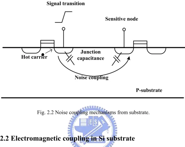
The second source of substrate noise is the capacitive coupling from drain or source node of the MOS transistor. As it is shown in Fig. 2.2, a digital switching device induces currents to substrate through the depletion capacitances of the p-n junction. Therefore, the amount of capacitive coupling noise will be larger as the transient time becomes faster. On the other hand, the parasitic capacitance induced by the interconnect is also added to the junction capacitance of source-drain and then causes the more severe coupling effect.
The third origin of substrate noise is the impact ionization. The importance of noise caused by impact ionization depends on the CMOS technology. When the CMOS technology goes to deep submicron level, the impact-ionization current have
Power line Power line Bounding wire inductance Chip Bounding pad
source of noise injection [3].
Fig. 2.2 Noise coupling mechanisms from substrate.
2.2 Electromagnetic coupling in Si substrate
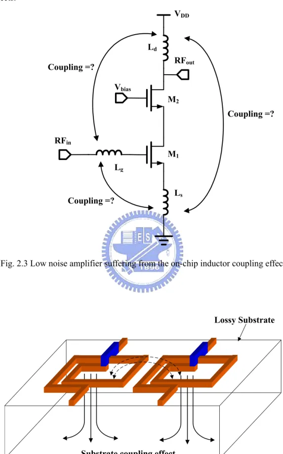
From Section 1.1, because of the concept of SOC, the integration of RF circuits in CMOS process is actively pursued in an effort to increase functionality and reduce cost. For the giga hertz frequency range, the electromagnetic coupling between RF circuit blocks through the lossy substrate is a concern. For example, the large RF signal power produced by a power amplifier will pass through the substrate and then affect the other sensitive circuit. Moreover, the on-chip inductors are often used in RF circuit designs, such as the low noise amplifier, band-pass filter, and mixer. As shown in Fig. 2.3 and Fig. 2.4, the electromagnetic coupling between two closely placed interconnects or inductors is also a way that induces the electromagnetic coupling in RFICs (Fig. 2.3). Therefore, if high-frequency coupling effects are not taken into account, the RF circuit performance will be degraded by these unwanted coupling
Signal transition
Sensitive node
Hot carrier capacitanceJunction
Noise coupling
effects.
Fig. 2.3 Low noise amplifier suffering from the on-chip inductor coupling effect.
Fig. 2.4 Coupling effect of two adjacent inductors.
Substrate coupling effect
Lossy Substrate M2 M1 Ls Lg Ld RFin RFout Coupling =? Coupling =? Coupling =? VDD Vbias
CHAPTER 3
Investigation of RF Spiral Inductor’s Coupling
Effects in Lossy Substrate
In this chapter, the coupling effects of two adjacent coplanar spiral inductors are investigated. First, the manufacturing process of the inductor is provided by NCTU Nano Facility Center (國立交通大學奈米中心). The process is different from the standard CMOS process utilized by TSMC or UMC. Second, the inductor coupling structure is proposed and the simulation results are shown. Finally, the measurement data and proposed model of inductor coupling effect are also obtained.
3.1 Design consideration of a single inductor
3.1.1 The fabrication process of the inductor
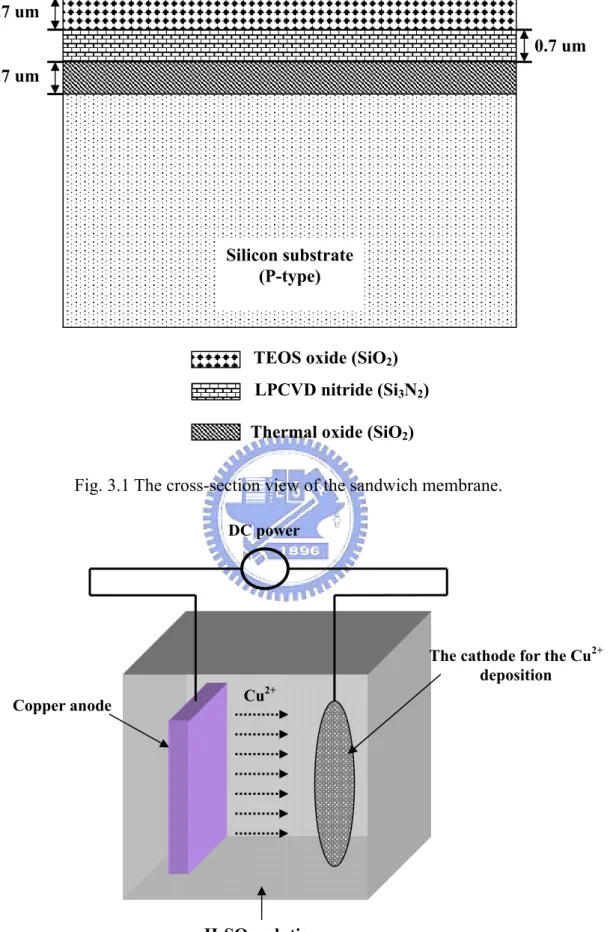
As mention before, the process is provided by NCTU Nano Facility Center; the process is quite different from the commercial process, such as TSMC or UMC standard CMOS process. The wafer is the 4 inch P-type doped wafer with a substrate resistivity of 21~23 Ω/cm. In order to get a good electrical performance, a sandwiched type membrane consisted of 0.7um thermal oxide, 0.7um LPCVD Si3N4, and 0.7um
TEOS oxide is employed (SiO20.7um/Si3N40.7um/SiO20.7um, [4]). The cross-section
view of these oxide layers are shown in Fig. 3.1 and the advantages of the proposed sandwiched structure are illustrated as the follows:
(1) Low dielectric loss: Because of the low conductivity and loss tangent properties, these dielectric layers have the low electromagnetic energy loss.
(2) Stress issue: The Young’s modulus of Si3N4 is five times larger than that of SiO2
(Table 3.1); the Si3N4 layer has the much higher residual stress with the silicon
substrate in comparison with SiO2. However, if proposed sandwiched structure is
utilized, the nitride stress can be effectively released by using the double oxide layers.
Table 3.1 Young’s modulus.
Material
Parameter SiO2 Si3N4
Young’s modulus (GPa) 73 310
The copper is utilized to form the metal strip of inductor. The metal is deposited above oxide layer by using electroplating method with the H2SO4 plating bath and the
copper anode. The total reaction of the plating procedure can be written as: Cu
e Cu2+ +2 − →
(3.1) The setup of the electroplating method is presented inFig. 3.2.
Fig. 3.1 The cross-section view of the sandwich membrane.
Fig. 3.2 The setup of the electroplating method.
Cu2+
Copper anode
The cathode for the Cu2+
deposition DC power H2SO4 solution Silicon substrate (P-type) 0.7 um 0.7 um 0.7 um
TEOS oxide (SiO2)
LPCVD nitride (Si3N2)
3.1.2 Specification of spiral inductor
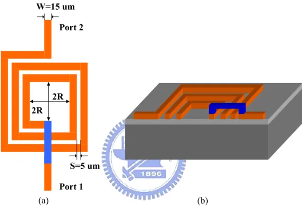
The size of the spiral inductor is shown in Fig. 3.3. Due to the process limitation, the space between two adjacent metal lines is 5um, the metal width and thickness are 15 um and 5 um, respectively. And the inner radius of the inductor is 60um. The graphical structure and design specifications are given in Fig. 3.3.
Fig. 3.3 Structure drawing of the inductor: (a) Top view. (b) Cross-section view.
3.2 Measurement results and modeling of a single inductor
3.2.1 Measurement setup
The S-parameters of a spiral inductor is measured by Agilent 8364B network analyzer and two GSG coplanar probes. The measurement setup is illustrated in Fig. 3.4 and the frequency range of measurement is from 0.1 GHz to 30 GHz.
S=5 um 2R 2R (a) (b) W=15 um Port 1 Port 2
Fig. 3.4 Measurement setup of the single inductor.
3.2.2 De-embedding procedure
To obtain a precise measurement of the inductor S-parameter, the paracitic effects of GSG pad are needed to be removed. Therefore, a process called “de-embedding” should be done after the complete two-port calibration. A de-embedding procedure that contains the open circuit and short circuit method (OSD) [5] is used in the measurement of inductor S-parameter. The paracitics of GSG pads are illustrated inFig. 3.5; the pad parasitic is lumped as yp and the parasitic due to pad
and probe tip interface discontinuity is modeled as Zi. After the parasitics are defined,
the Zi and yp are extracted by the short and open test pattern. Therefore, the
S-parameters of single inductor without pad parasitics can be obtained by transmission matrix operation. The de-embedding procedure can be written as the follows:
(
inopen inshort)
p short in i Z Z y Z Z , , , 1 − = =The transmission matrix (T) of DUT (Device Under Test) can be derived [6]:
GSG Probe
G
G
G
G
[ ]
[ ]
[ ]
[ ] [ ] [ ] [ ] [ ]
[ ]
[ ] [ ] [ ] [ ] [ ]
[ ]
= = ⇒ = ⇒ = = − − − − D C B A T and T T T T T T T T T T T T y T Z dut y Z Z y Z y DUT y Z measure p y i Z p i measure i p DUT i p p i p i , 1 0 1 , 1 0 1 T 1 1 1 1Therefore, the S-parameters of the DUT can be obtained from
[ ]
T DUT[ ]
Ω = + + + + − + − = + + + = + + + − = + + + − − + = = 50 and , 50 / / , / 2 / ) ( 2 , 50 / / Where , 0 0 0 0 22 0 0 21 0 0 12 0 0 0 11 22 21 12 11 Z D CZ B A D CZ Z B A S D CZ Z B A S D CZ Z B A BC AD S D CZ B A D CZ Z B A S S S S S S DUTFig. 3.5 Parasitic of GSG pad and pad parastics extraction. (a) The equivalent circuit model of pad parasitic. (b) The extraction method of pad parasitic.
DUT yp Zi Zi yp Termination (50Ω
)
Termination (50Ω)
Zin,short Zi yp Zi Termination (50Ω) Termination (50Ω) Zin,open (a) (b)3.2.3 Measurement results and equivalent circuit model of spiral inductor
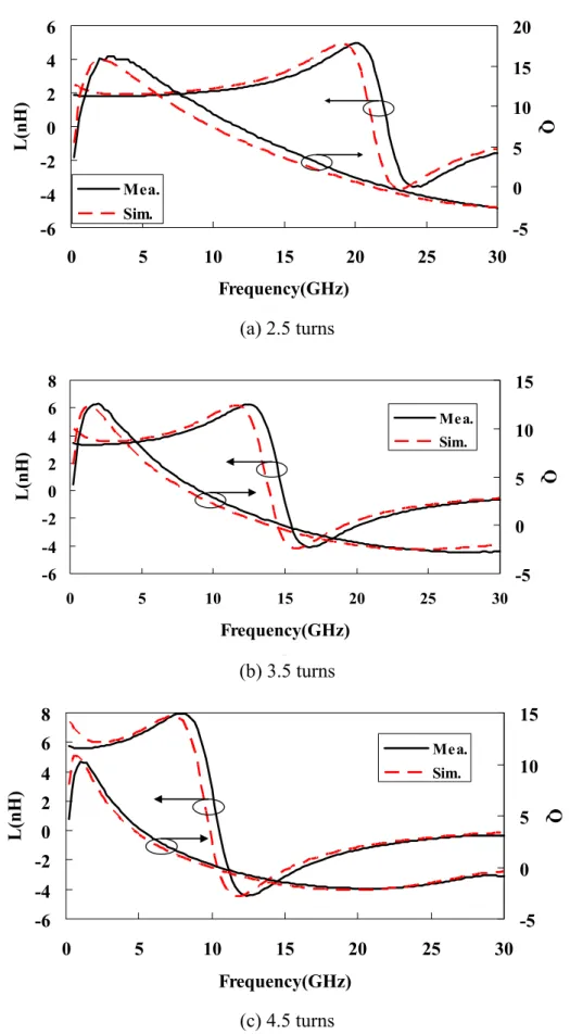
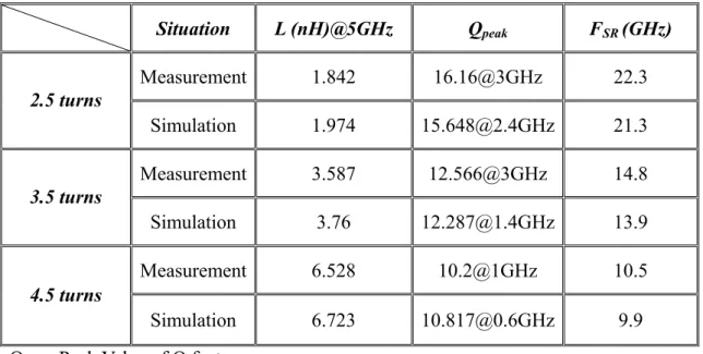
In reference to the micrograph of a 3.5 turns spiral inductor as shown in Fig.3.6 and the comparisons between measurement (Mea.) and simulation (Sim.) results using Ansoft HFSS are shown in Fig. 3.7 with a good agreement. Moreover, the effective inductance of 2.5 turns, 3.5 turns, and 4.5 turns inductor are 1.842 nH, 3.587 nH, and 6.528 nH, respectively, and the peak value of Q factor for 2.5 turns, 3.5 turns, and 4.5 turns inductor are 16.16, 12.566, and 10.2, respectively. The deviation of effective inductance and Q factor between simulation and measurement are within 8%. Furthermore, the measured self resonant frequency (FSR) of 2.5 turns, 3.5 turns and4.5 turns inductor are 22.3, 14.8, and 10.5 GHz, respectively. In comparison with simulated self resonant frequency is at 21.3 GHz, 13.9 GHz, and 9.9 GHz for 2.5 turns, 3.5 turns, and 4.5 turn inductor, respectively. The FSR of simulation is 1 GHz lower
than measurement data. Finally, the measurement and simulation results are summarized in Table 3.2.
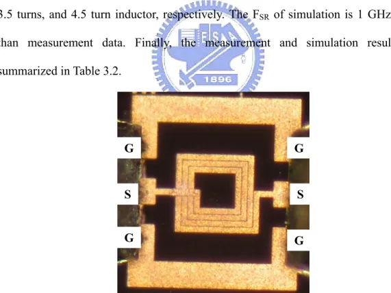
Fig. 3.6 Inductor micrograph (3.5 turns).
G G G G S S
-6 -4 -2 0 2 4 6 0 5 10 15 20 25 30 Frequency(GHz) L(n H ) -5 0 5 10 15 20 Q Mea. Sim. (a) 2.5 turns -6 -4 -2 0 2 4 6 8 0 5 10 15 20 25 30 Frequency(GHz) L(n H ) -5 0 5 10 15 Q Mea. Sim. (b) 3.5 turns -6 -4 -2 0 2 4 6 8 0 5 10 15 20 25 30 Frequency(GHz) L(nH) -5 0 5 10 15 Q Mea. Sim. (c) 4.5 turns
Table 3.2 Summary of inductors (measurement and simulation). Situation L (nH)@5GHz Qpeak FSR (GHz) Measurement 1.842 16.16@3GHz 22.3 2.5 turns Simulation 1.974 15.648@2.4GHz 21.3 Measurement 3.587 12.566@3GHz 14.8 3.5 turns Simulation 3.76 12.287@1.4GHz 13.9 Measurement 6.528 10.2@1GHz 10.5 4.5 turns Simulation 6.723 10.817@0.6GHz 9.9
Qpeak: Peak Value of Q factor.
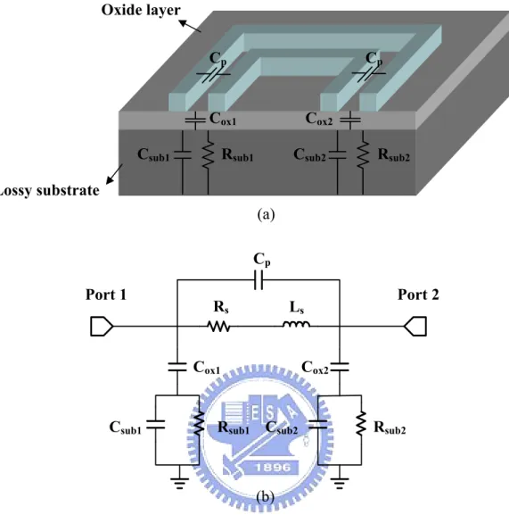
After getting the measurement data of inductor, a model is established and then used it to fit the measurement results. The traditional π model is presented in Fig. 3.8 and the meaning of the components for the equivalent circuit model is illustrated as the follows:
(1) Cp: Capacitance between adjacent metal lines.
(2) Rs: Resistance of metal line.
(3) Ls: Inductance of metal line.
(4) Cox1, Cox2: Capacitance between metal line and substrate.
(5) Csub1, Csub2: Parasitic capacitance of lossy substrate.
Fig. 3.8 Equivalent circuit model of the analyzed spiral inductor. (a) 3-D view. (b) Whole equivalent circuit model of the π model.
Furthermore, in order to extract these parameters of π model, a procedure is proposed to make the extraction more efficient. The procedure of parameter extraction is outlined in the following steps:
Step1. Rs and Ls: According to the equivalent model of the inductor, all the parasitic
capacitances are opened as the frequency is low. Therefore, the Rs and Ls are
extracted from the Y-parameters of the measurement results at the low
Rsub2 Csub2 Rsub1 Csub1 Cox1 Cox2 Cp Cp Oxide layer Lossy substrate (a) Cp Rs Ls Cox1 Cox2
Csub1 Rsub1 Csub2 Rsub2
Port 1 Port 2
by Rs= 11 1 y real and Ls= frequency y imag × π 2 ) / 1 ( 11 (3.2)
Where real= Real part and imag = imaginary part.
Step2. Cp: The parameter Cp is extracted from the y21 for the equivalent circuit model
as shown in Fig. 3.9. From Fig. 3.9, the resonant frequency is given at
p sC L π 2 1
and the Cp is read as:
(
2)
, 21 1 y of frequency resonant self f L f C SR s SR p = π = (3.3)Fig. 3.9 Equivalent circuit of y21.
Step3. Rsub1, Rsub2, Csub1, and Csub2: The parasitics of the lossy substrate start to
affect the inductor as the frequency increases. Therefore, the Cox1 and Cox2 are
neglected, and the equivalent circuit becomes Fig. 3.10. From Fig. 3.10, we can write:
(
)
s s sub p sub in R L j R C C j port Y + + + + = ω ω 1 1 ) 1 ( 1 1 (3.4)At the resonant point, we can obtain:
I2
V1 Cp
Rs Ls
Cox1
(
)
+ = = = + = + = (3.5b) 1 1 ) 1 ( 1 (3.5a) ) 1 ( , 2 1 1 1 2 2 2 s sub f s sub in in SR p sub s SR s s f L R C R R port Y real R port Y of frequency resonant f C C L f R L CSR πWe suppose the Rsub1 is small and neglect the error term
s sub f s L R C R 1 and give
(
2)
(3.6b) (3.6a) ) 1 ( 1 2 2 2 1 1 − + = ≅ = p s SR s sub f f sub C L f R Ls C port Yin real R SR πFurthermore, we use the same method to get the Rsub2 and Csub2 values as we
change the Yin from port 1 to port 2.
Fig. 3.10 Input admittance (Yin) of port 1.
Step4.Cox1 and Cox2: The parallel plate capacitor formula is utilized to derive the Cox1
and C . The parallel plate formula is written as:
Cp Rs Ls Rsub1 Csub1 Yin (port 1)
plates parallel o between tw distance the d plates parallel two e between th filled is that constant dielectric ε plate parallel the of area A , = = = = d A C ε
After the initial values of the model are gained, the optimal function of the simulation tool (Agilent ADS) is utilized to obtain the final values of the equivalent circuit model.
However, the traditional π model only can fit the measurement data up to 15 GHz. Hence, in order to get a wide band frequency response (up to 30 GHz), the high frequency parasitic of the lossy substrate are taken into account and some components(Rsub3, Csub3, Lsub1, Lsub2) are added to match the high frequency
S-parameters of measurement data [7]-[9]. Therefore, the whole equivalent circuit of the wide band inductor model is shown in Fig. 3.11. As shown in Fig. 3.11, the Lsub1
and Lsub2 are used to model the inductive parasitic of the lossy substrate, and Rsub3 and
Csub3 describe another signal path from port 1 to port 2 when the frequency goes to
high. Therefore, if these components are added in the traditional π model, a good agreement between modeling and measurement results can be obtained in the frequency range from 0.2 GHz to 30 GHz.
Fig. 3.11 The broad band equivalent model of spiral inductor.
Furthermore, the effective inductance and Q factor of measurement and modeling results of a spiral inductor are presented in Fig. 3.12. Form Fig. 3.12, the effective inductance of proposed inductor model is almost identical to the measurement results. And the Q factor of the model is a little large than measurement. Finally, Table 3.2 and Table 3.3 give the component list of wide band inductor model and a summary between measurement, HFSS simulation, and modeling results of the varying spiral inductors, respectively.
Cp
Ls
Rs
Cox1 Cox2
Csub1 Rsub1 Csub2 Rsub2
Lsub1 Lsub2
Rsub3
Csub3
-6 -4 -2 0 2 4 6 0 5 10 15 20 25 30 Frequency(GHz) L(nH) -5 0 5 10 15 20 Q Mea. Model (a) 2.5 turns -6 -4 -2 0 2 4 6 8 0 5 10 15 20 25 30 Frequency(GHz) L( nH) -5 0 5 10 15 Q Mea. Model (b) 3.5 turns -6 -4 -2 0 2 4 6 8 0 5 10 15 20 25 30 Frequency(GHz) L(nH) -5 0 5 10 15 Q Mea. Model (c) 4.5 turns
Fig. 3.12 Measurement (Mea.) and modeling (Model) results of inductors. (a) 2.5 turns. (b) 3.5 turns. (c) 4.5 turn.
Table 3.3 Component list of the wide band inductor equivalent model. 2.5 3.5 4.5 Ls(nH) 1.73 3.232 5.422 Rs(Ω) 0.977 1.486 1.965 Cp(fF) 8.255 12.037 13.679 Cox1(fF) 242.824 313.848 426.241 Cox2(fF) 307.679 394.457 495.442 Rsub1(Ω) 1386.31 1110.61 978.768 Rsub2(Ω) 1209.78 930.016 708.827 Csub1(fF) 25.284 22.147 25.284 Csub2(fF) 25.312 33.263 41.723 Rsub3(Ω) 5218.28 4526.167 4340.981 Csub3(fF) 1.079 1.555 1.833 Lsub1(nH) 0.246 0.631 0.979 Lsub2(nH) 0.21 0.439 0.616 Size Turns
Table 3.4 Summary of the spiral inductor. Situation L (nH)@5GHz Qpeak FSR (GHz) Measurement 1.842 16.16@3GHz 22.3 Simulation 1.974 15.648@2.4GHz 21.3 2.5 turns Modeling 1.810 18.427@3.2GHz 22.1 Measurement 3.587 12.566@3GHz 14.8 Simulation 3.76 12.287@1.4GHz 13.9 3.5 turns Modeling 3.609 13.327@1.8GHz 14.7 Measurement 6.528 10.2@1GHz 10.5 Simulation 6.723 10.817@0.6GHz 9.9 4.5 turns Modeling 6.582 11.11@1.2GHz 10.7
3.3 Analysis of inductor coupling effects
In RF integrated circuits (RF ICs), such as LNA, mixer, and band-pass filter, the inductor is a key element for circuit designs. Unfortunately, because the substrate is lossy, the coupling effect in giga hertz frequency range is a big issue (Fig. 2.3 and Fig. 2.4). In this section, two types of inductor coupling situations are proposed (as shown in Fig.3.13) and their coupling mechanisms for different distance (d) are studied.
Fig. 3.13 Two type of inductor coupling situations.
3.3.1 Measurement setup and de-embedding method
The measurement instrument is the Agilent 8364B network analyzer. However, the inductor coupled pair is a four-port network, so a pair of GSGSG probes is utilized and the Agilent 8364B 4-port measurement function is used to get the 4× 4 S-parameters matrix of the structure. The measurement setup is shown in Fig. 3.14.
d d
Port1 Port2
Port 3
Port 4 Port 4 Port 3
Port1 Port2
Fig. 3.14 Measurement setup of the inductor coupled pair.
As mention before, the de-embedding procedure must be done after measurement. The de-embedding procedure is almost same as stated in Section 3.2.2. The only difference is that we expand the 2× matrix to 2 4× matrix. The de-embedding 4 formulas are derived as:
[ ]
[ ] [ ] [ ] [ ] [ ]
[ ]
[ ] [ ] [ ] [ ] [ ]
then T T T T T T T T T T T T i measure i p DUT i p p i Z Z y Z y DUT y Z measure 1 1 1 − − − = =[ ]
= 4 3 2 1 4 3 2 1 4 3 2 1 4 3 2 1 d d d d c c c c b b b b a a a a T DUT (3.7)And the 4× S-parameters matrix becomes: 4
G G G G G G S S S S Port 1 Port 2 Port 3 Port 4
[ ]
(3.9p) , ) )( ( ) )( ( (3.9o) , ) )( ( ) )( ( (3.9n) , ) ( 2 (3.9m) , ) ( 2 (3.9l) , ) )( ( ) )( ( (3.9k) , ) )( ( ) )( ( (3.9j) , ) ( 2 (3.9i) , ) ( 2 (3.9h) , ) )( ( ) )( ( ) )( ( (3.9g) , ) )( ( ) )( ( ) )( ( (3.9f) , ) )( ( ) )( ( (3.9e) , ) ( 2 (3.9d) , ) )( ( ) )( ( ) )( ( (3.9c) , ) )( ( ) )( ( ) )( ( (3.9b) , ) ( 2 (3.9a) , ) )( ( ) )( ( (3.8) , 7 3 6 2 3 7 6 2 44 5 1 6 2 1 5 6 2 43 6 2 42 6 2 41 3 7 8 4 7 3 8 4 34 1 5 8 4 5 1 8 4 33 8 4 32 8 4 31 6 3 7 2 8 4 8 3 7 4 6 2 6 4 8 2 7 3 24 6 1 5 2 8 4 8 1 5 4 6 2 6 4 8 2 5 1 23 6 2 8 4 4 8 6 2 22 8 2 6 4 21 8 2 6 4 7 3 6 3 7 2 8 4 8 3 7 4 6 2 14 8 2 6 4 5 1 4 5 8 1 6 2 6 1 2 5 8 4 13 6 4 8 2 12 8 4 6 2 2 6 8 4 11 44 43 42 41 34 33 32 31 24 23 22 21 14 13 12 11 ∆ − + + − + = ∆ − + + − + = ∆ + − = ∆ + = ∆ − + + − + = ∆ − + + − + = ∆ + = ∆ + − = ∆ + + + + + − − − = ∆ + + + + + − − − = ∆ − + + − + = ∆ − = ∆ − − + + + − + + = ∆ − − + − + + − + = ∆ − = ∆ − + + − + = = f f k k k k f f S f f k k k k f f S k k S f f S f f k k k k f f S f f k k k k f f S k k S f f S f f f f k k f f f f k k f f f f k k S f f f f k k f f f f k k f f f f k k S f f k k f f k k S f f f f S k k k k f f k k k k f f k k k k f f S k k k k f f k k k k f f k k k k f f S k k k k S k k f f k k f f S Where S S S S S S S S S S S S S S S S S DUT Where ∆= (k8+k4) (f6+f2).(k6+k2) (f4+f8)50 Z , , , , , and , , , 0 2 0 4 8 0 4 2 4 2 0 4 8 0 4 2 4 2 0 4 7 0 4 2 3 2 0 4 7 0 4 2 3 1 0 3 6 0 3 1 2 1 0 3 6 0 3 1 2 1 0 3 5 0 3 1 1 1 0 3 5 0 3 1 1 Ω = + = + = + = + = − = − = − = − = + = + = + = + = − = − = − = − = d Z d f Z b b f c Z c k Z a a k d Z d f Z b b f c Z c k Z a a k d Z d f Z b b f c Z c k Z a a k d Z d f Z b b f c Z c k Z a a k and
The formulas above are only the summarized results, and a complete derivation process can be referred to Appendix I.
3.3.2 Measurement results of inductor coupled pairs
The micrograph of inductor coupling pairs and measured S-parameters of type B inductor coupling pairs are presented in Fig. 3.15 and Fig. 3.16, respectively. The S41
of the inductor coupled pairs is taken as the amount of substrate coupling effect between two inductors. As shown in Fig. 3.16, the S41 is decreasing when d is
increasing. And the measurement results conform to our prediction. Therefore, the inductor coupling effect will reduce if the distance between two inductors is increased. After the measurement data is obtained, the comparison between the simulation and measurement results is done and found out the measurement data reasonable or not. And the simulation tool is Ansoft HFSS, too. From Fig. 3.16, the measured S41 is
lower then simulation and the maximum deviation of S41 is less than 1 dB. Therefore,
the good agreement between measurement and simulation is obtained. Furthermore, to inspect the S41 value of 2.5 turns inductor coupled pairs and 3.5 turns inductor
coupled pairs, it can be observed the S41 is slightly dependent on the frequency.
Moreover, the differences of S41 for different types of inductor coupled pairs are
phenomenon is because that the inductor coupled pairs of type B has the longer metal lines in opposition to each other. As a result, the metal line induces the larger coupling effect between two inductors. Furthermore, the magnetic flux of type B is larger than that of type A; it is also a reason that the S41 value of type B is larger than that of type
A.
Fig.3.15 Micrograph of inductor the coupling pair (3.5 turns typeB with d=30um).
G
G
G
G
G G
S S
S S
-40 -35 -30 -25 -20 0 5 10 15 20 Frequency(GHz) S4 1( dB ) 30um(Mea.) 50um(Mea.) 75um(Mea.) 100um(Mea.) 30um(Sim.) 50um(Sim.) 75um(Sim.) 100un(Sim.) (a) -40 -35 -30 -25 -20 0 5 10 15 20 Frequency(GHz) S 41( d B ) 30um(Mea.) 50um(Mea.) 75um(Mea.) 100um(Mea.) 30um(Sim.) 50um(Sim.) 75um(Sim.) 100un(Sim.) (b)
Fig. 3.16 Measurement (Mea.) and simulation (Sim.) result of the inductor coupled pairs for the varying separate distance. (a) 2.5 turns, type B. (b) 3.5 turns, type B.
-45
-40
-35
-30
-25
-20
0
5
10
15
20
Frequency(GHz)
S4
1(
dB
)
3B3 3B5 3B7 3A3 3A5 3A7 Notes:(1) 3.5 turns type A (2) 3.5 turns type B d=30um: 3A3 d=30um: 3A3 d=50um: 3A5 d=50um: 3A5 d=75um: 3A7 d=75um: 3A7
Fig.3.17 Comparison of different types for 3.5 turns inductor coupled pairs.
3.3.3 Discussion about the inaccuracy between measurement and
simulation results
To compare the measurement and simulation results, the trend of simulation curve is similar to that of measurement, but the overall S41 values are about 1 dB
larger than measurement results for different distances. Hence, we attempt to find the 1dB variation between simulation and measurement results. We suppose that the source of variation comes from the process we used. First, the oxide thickness is confirmed, and the oxide thickness is almost equal with 2.1 um after measurement.
variation of S41 is within 0.1 dB. As a result, the effective dielectric constant is not the
main fact that can cause the S41 deviation. And the last, the conductivity of the wafer
is checked. The conductivity=4 (Siemens/m) is used in the simulation. But when the conductivity is changed from 4 to 5 (Siemens/m), the simulation curve is more similar to the measurement one. Fig. 3.18 and Fig. 3.19 present the improved simulation results and compare them with measurement curve for the 2.5 turns and 3.5 turns inductor coupled pairs, respectively. Therefore, the variation of conductivity of the wafer is the main factor that causes the variation between measurement and simulation results.
-40 -35 -30 -25 -20 0 5 10 15 20 Frequency(GHz) S41(d B ) 2B3(Mea.) 2B3_C4(Sim.) 2B3_C5(Sim.) (a) -40 -35 -30 -25 -20 0 5 10 15 20 Frequency(GHz) S4 1( dB ) 2B5(Mea) 2B5_C4(Sim.) 2B5_C5(Sim.) (b) Notes: (1) 2.5 turns, type B
d=30 um, conductivity of wafer=4 (Seimens/m): 2B3_C4 d=30 um, conductivity of wafer=5 (Seimens/m): 2B3_C5 d=50 um, conductivity of wafer=4 (Seimens/m): 2B5_C4
d=50 um, conductivity of wafer=5 (Seimens/m): 2B5_C5
-40 -35 -30 -25 -20 0 5 10 15 20 Frequency(GHz) S41(d B ) 3B3(Mea.) 3B3_C4(Sim.) 3B3_C5(Sim.) (a) -40 -35 -30 -25 -20 0 5 10 15 20 Frequency(GHz) S4 1( dB ) 3B5(Mea.) 3B5_C4(Sim.) 3B5_C5(Sim.) (b) Notes: (1) 3.5 turns, type B
d=30 um, couductivity of wafer=4 (Seimens/m): 3B3_C4 d=30 um, couductivity of wafer=5 (Seimens/m): 3B3_C5 d=50 um, couductivity of wafer=4 (Seimens/m): 3B5_C4 d=50 um, couductivity of wafer=5 (Seimens/m): 3B5_C5
Fig.3.19 Improved simulation (Sim.) and measurement (Mea.) results for the 3.5 turns type B inductor coupled pairs. (a) d=30um. (b) d=50um.
3.3.4 Modeling of inductor coupled pairs
Having acquired the measurement data of inductor coupled pairs; a model is constructed to represent their noise coupling behavior. First, a RC parallel network (Rsub4, Rsub5, Csub4, and Csub5) is established to describe the electrical noise coupling
effect in the lossy substrate. Second, the coupling coefficient (k) is exploited and it can express the magnetic coupling effect between two inductors. Finally, these two parts are combined with the wide band inductor model and the whole equivalent circuit model is presented in Fig. 3.20.
Fig. 3.21 shows the modeling results of 2.5 turns type B inductor coupling pair, and the meaning of 2B3, 2B5, and 2B7 are corresponding to d=30um, d=50um, d=75um, respectively. As observed in Fig. 3.21, the difference between modeling and measurement results is only within 0.3 dB. Moreover, the proposed model can represent the curve of coupling effect from 1 GHz~15 GHz and the component values of the coupling circuit is listed in Table 3.4.
Moreover, the scaling formulas of the inductor coupled pairs are also derived from the extracted parameters (Rsub4, Rsub5, Csub4, Csub5, and k). And the formulas are
shown as the follows:
Rsub4=-0.129d2+57.778d+3630.7 (Ω) (3.10a) Rsub5=-0.3949d2+89.275d+2311.5 (Ω) (3.10b) Csub4=-0.0624d+7.352 (fF) (3.10c) Csub5=-0.0601d+6.9979 (fF) (3.10d) k=-0.0007d+0.2025 (3.10e) d=um
Fig. 3.20 Equivalent circuit of the inductor coupled pairs. Cp Rs Ls Cox2 Rsub3 Csub4 Cox1 Rsub2 Rsub2 Csub2 Csub2 Rsub1 Csub1 Csub1 Rsub1 Lsub1 Lsub1 Lsub2 Lsub2 Rsub3 Csub3 Rsub4 Csub3 Rsub5 Csub5 Cox2 Cox1 Rs Ls Cp Coupling coefficient k Port 1 Port 3 Port 2 Port 4
(1) The definition of ports is the same with Fig.3.12
(2) Csub4||Rsub4: The electrical noise coupling between Port 1and Port 2
(3) Csub5||Rsub5: The electrical noise coupling between Port 3and Port 4
-40 -35 -30 -25 -20 0 3 6 9 12 15 Frequency(GHz) S4 1( dB ) Mea. Model (a) -40 -35 -30 -25 -20 0 3 6 9 12 15 Frequency(GHz) S 41( d B ) Mea. Model (b)
-40 -35 -30 -25 -20 0 3 6 9 12 15 Frequency(GHz) S4 1( dB ) Mea. Model (c) (d) Note: (1) 2.5 turns type B d=30um: 2B3 d=50um: 2B5 d=75um: 2B7 d=100um: 2B1
Fig. 3.21 Measurement (Mea.) and Modeling (Model) results. (a) 2B3. (b) 2B5. (c) 2B7. (d) 2B1. -40 -35 -30 -25 -20 0 3 6 9 12 15 Frequency(GHz) S41( dB ) Mea. Model
Table 3.5 Component list of the equivalent circuit of 2.5 turns type B inductor coupled pairs. d(um) Component 30 50 75 100 Rsub4(Ω) 5281.7 6111.07 7312.56 8090.65 Rsub5(Ω) 4609.75 5849.66 6730..65 7307.25 Csub4(fF) 5.34 4.492 2.549 1.12 Csub5(fF) 5.165 4.113 2.225 1.09 k 0.1818 0.1643 0.1493 0.13
3.4 Comparison with other works
When the measurement and modeling results is done, we try to compare the results with the publication data. First, from [10] and [11], the measurement method is the two-port measurement case with the other terminals being open or floating (as depicted in Fig.3.22). On the contrary, our measurement data are the four-port S-parameters matrix with all ports at the 50 Ω terminations. Those measurement data are more useful for RF circuit designers to apply them for the post-simulation procedure before the chip tape out.
Moreover, in the part of proposed equivalent circuit of inductor coupled pairs, the frequency range is up to 15 GHz with the deviation of 0.3 dB. According to [11], its frequency range of equivalent model is only about 10 GHz and the deviation between measurement and model is larger than 1 dB. As a result, the proposed model can explore the coupling effect of inductor coupled pairs more accurately.
Fig. 3.22 Sketch of the inductor coupling pair in [10].
Fig. 3.23 Sketch of the inductor coupling pair in [11].
Table 3.6 Comparison with other papers.
This work Ref.[10] Ref.[11]
Process Home-made process on 21-23Ω-cm P-type substrate 0.25um, 5-level metal, CMOS process
on 10Ω-cm p-type substrate 0.25um, 4-level metal, logic-CMOS process on 10Ω-cm P-type substrate
Measurement Full four ports Two ports (other ports floating)
Two ports (other ports floating)
Modeling 1 GHz -15 GHz N/A 1 GHz -10 GHz
Error
(Sim. and Mea.) About 1dB N/A N/A Error
(Mea. and Model.)
0.3 dB About 1dB N/A
N/A: Not available.
Port 1 floating
Port 4 floating Port 2
Port 3
d
d
3.5 Summary and contributions
In Section 3.2, the wide band model for spiral inductor is proposed and the improved model represents the good agreement from 0.2 GHz to 30 GHz. Moreover, the coupling effect of two inductors is discussed in Section 3.3. The simulation method can predict the coupling effect precisely with the error of 1 dB between the simulation and measurement results. Utilizing the simulation method can understand the coupling effect between inductors. Thus, the circuit designers can use the method to avoid the unwanted coupling effect during the circuit design procedure.
Besides, the equivalent model of inductor coupled pairs is also proposed. The equivalent circuit model shows the good performance in the range of 1 GHz -15 GHz. This is also the useful information for RF circuit designers.
Finally, the contributions and differentiations from the other papers are summarized as the follows:
(1) A full four ports simulation, de-embedding, and measurement procedure for inductor coupling is done. The papers ([10] and [11]) are only the two-port measurement results with other ports being floating. Moreover, a good agreement between the simulation and measurement data is obtained in our study.
(2) The equivalent circuit of 2.5 turns type B inductor coupled pairs is established in the frequency range of 1 GHz to 15 GHz. Besides, the equivalent circuit takes the electrical and magnetic parasitics into account at the same time.
CHAPTER 4
Substrate Noise Coupling Effect in TSMC 0.18um
CMOS Process
In this chapter, the substrate coupling effects in TSMC 0.18um CMOS process are studied. First, the testkey is designed to investigate the substrate coupling effect between two P+(or N+) contacts in N-well (or P-well). Furthermore, the distance between two contacts is changed and it can find the substrate coupling effect for different distance. Therefore, the behavior of noise propagating in the lossy silicon substrate can be realized.
4.1 Testkey design
In the testkey, several types of test patterns are designed to study the substrate coupling effect in different well (P-well and N-well). As presented in Fig. 4.1, two P+ (or N+) contacts are formed with area=15×15 um2 in P-well (or N-well), and then vary
the distance (d) between two contacts to observe the amount (S21 of the two-port
network) of substrate coupling effect. Thus, the propagation of substrate noise in the lossy substrate can be observed. Moreover, a summary of the testkey is listed in Table 4.1.
(a)
(b)
Fig. 4.1 Structure of the test pattern. (a) Cross-section view. (b) Top view.
Table 4.1 Specification of the testkey.
P-well N-well d(um) N+~N+ P+~P+ 50 ● ● 75 ● ● 100 ● ● 125 ● N/A
N/A: Not available.
15um 15um
d
P-substrate
P-well (or N-well) N+ Port 1 Port 2 N+ 15um 15um 20um 20um
P-well (or N-well) Port 2 Port 1
4.2 Measurement results
The micrograph of the testkey is shown in Fig. 4.2. The row 1 and row 4 are the test patterns. The measurement setup is presented as Fig. 4.3 and the Agilent 8364B network analyzer and a pair of GSG probes with pitch size 100 um are used during measurement. Therefore, The S21 measurement results of the two-port network as the
quantity of substrate noise in substrate, the substrate noise as shown in Fig. 4.4 is reducing when the distance(d) becomes longer. And the relationship between quantity of noise coupling and distance seems to be linear. Moreover, the measurement data show the quantity of substrate noise coupling is almost independent of frequency. Therefore, the measurement results imply that substrate noise coupling effect is almost resistive in the lossy substrate.
Fig. 4.2 Micrograph of the testkey.
N.well with P+ contact
P.well with N+ contact
(a)
(b)
Fig. 4.3 Measurement setup. (a) Connect to network analyzer. (b) Test pattern (P-well with N+ contact and d=125 um) with probing.
Agilent 8364B P+ P+ N-well P-substrate G G G G S S
-60 -55 -50 -45 -40 -35 -30 0 5 10 15 20 Frequency(GHz) S21( dB ) 50um 75um 100um 125um (a) -50 -45 -40 -35 -30 -25 0 5 10 15 20 Frequency(GHz) S2 1( dB) 50um 75um 100um (b)
CHAPTER 5
Conclusion and Future Works
5.1 Conclusion
In the thesis, the coupling effect of two adjacent inductors is presented first. Moreover, a wide band model of single spiral inductor is also built up. The inductor model can fit the effective inductor and Q factor from 0.2 GHz to 30 GHz in correlation with the measurement. In the part of inductor coupled pairs, the measurement data indicate the coupling effect between two inductors is less than -20dB. Moreover, we also realize the coupling effect of inductor coupled pairs is slightly dependent on the separate distance. As a result, to increase the distance and suppress the noise coupling effect between two inductors is not an efficient way.
From the measurement results of type A and type B, the quantity of S41 are not
equal. The results give a hint that the coupling effect is related to the layout style of inductors. And the proper layout style can reduce the coupling effect of adjacent inductors. After the measurement results of inductor coupled pairs are obtained, an equivalent circuit model is established to illustrate the coupling effect. The proposed model can precisely predict the coupling behavior from 1 GHz to 15 GHz.
The substrate noise coupling phenomenon in TSMC 0.18um CMOS process is discussed, too. In this part, the substrate coupling effect of two P+ (or N+) contacts in N-well (P-well) is analyzed. According to the measurement result, we find the substrate coupling effect is not strongly dependent on the frequency.
for RF circuit designers. The designers can refer to the information and decrease the parasitic effect of inductors. Therefore, a more efficient RF circuit design procedure can be realized.
5.2 Future works
As the model established in Section 3.3.4, the model of inductor coupling can explore the coupling behavior from 1 GHz to 15GHz. The frequency range is not wide enough for RF circuit designers. As a result, how to increase the frequency range is the most important thing to do.
Moreover, the inductor coupled pairs used in RF circuit designs is not only the type we propose. There are many different layout styles of inductor coupled pairs. Hence, to find their coupling mechanisms and sum up those results is the significant task, too
Finally, we investigate the substrate noise coupling effect in TSMC 0.18um CMOS process. The situation we investigate is passive like. The coupling effect of active device, such as MOSFET and BJT, is not discussed in the thesis. Therefore, as the operation frequency goes to high (up to 60 GHz), the study about the substrate noise coupling effect of active device is an urgent issue for RF circuit designs.
REFERENCES
[1] D. K. Su, M. J. Loinaz, S. Masui, and B. A. Wooley, “Experimental Result and Modeling Techniques for Substrate Noise in Mixed.signal Integrated Circuits,”
IEEE J. Solid-State Circuits, vol. 28, pp. 420-430, Apr. 1993.
[2] T. Gabara, “Reduced Ground Bounce and Improved Latch up Suppression through Substrate Condition,” IEEE J. Solid-State Circuits, vol. 23, pp. 1224-1232, Oct. 1988.
[3] R. B. Merrill, W. M. Young, and K. Brehmer, “Effect of Substrate Material in Mixed Analog/Digital Integrated Circuits,” in Proc. IEEE Int. Electron Devices
Meeting, pp. 433-436, San Francisco, CA, Dec. 1994.
[4] J. W. Lin, “An Optimum Design of the Micromachined RF Inductor” Master’s thesis, Dept. of Electronics Engineering and Inst. of Electronics, NCTU, Taiwan, 2004.
[5] Troels Emil Kolding, “On-Wafer Calibration Techniques for giga-hertz CMOS Measurement,” in Proc. ICMTS, pp.105.110, March 1999.
[6] D. M. Polar, Microwave Engineering, Third edition, John Wiley & Sons, Inc., 2005.
[7] C. J. Chao, S. C. Wong, C. H. Kao, M. J. Chen, L. Y. Leu, and K. Y. Chiu, “Characterization and Modeling of On-Chip Spiral Inductors for Si-RFICs,” IEEE
Trans. on semiconductor manufacturing, pp. 19-29, Feb. 2002.
[8] T. S. Horng, J. K. Jau, C. H. Huang, and T. Y. Han, “Synthesis of a Super Broadband Model for On-Chip Spiral Inductors,” IEEE RFIC Symposium, pp.453-456, June 2004.
vol. 51, pp. 2023-2028, Step. 2003.
[10] C. J. Chao, S. C. Wong, C. J. Hsu, M. J. Chen, and L. Y. Leu, “Characterization and Modeling of On-Chip Inductor Substrate Coupling Effect,” IEEE RFIC
Symposium, pp. 311-314, June 2002.
[11] A. O. Adan, M. Fukumi, K. Higashi, T. Suyma, M. Miyamoto, and M. Hayshi, “Electromagnetic Coupling Effects in RFCMOS Circuits,” IEEE RFIC
Symposium, pp. 293-296, June 2002.
[12] M. Werthen, I. Wolff, R. Keller,and W. Bischof, “Investigation of MMIC Inductor Coupling Effect,” IEEE MTT-S International, vol.3, pp. 1793.1796, June 1997.
Appendix I
Four-Port Transformation
Because considering the model for the pad parasitic as Zi and yp, the equivalent
circuit of our DUT (with pad parasitic) is shown in Fig. 1. Therefore, we derive the transmission matrix of the pad parasitic and use the de-embedding procedure to obtain the correct measurement result of our four-port network.
Fig. 1 The four-port network with pad parasitics.
Pad parasitics Zi yp Zi yp yp yp Zi Zi Port 1 Port 2 Port 3 Port 4 DUT
A. Transmission matrix of Z circuit
The Z circuit is presented in Fig. 2. From the definition of transmission matrix, we can derive that:
[ ]
T Zcircuit Z Z d d d d c c c c b b b b a a a a where I I V V d d d d c c c c b b b b a a a a I I V V 2 1 4 3 2 1 4 3 2 1 4 3 2 1 4 3 2 1 4 3 4 3 4 3 2 1 4 3 2 1 4 3 2 1 4 3 2 1 2 1 2 1 1 0 0 0 0 1 0 0 0 1 0 0 0 1 , = = = Fig. 2 Z circuit. B. Transmission matrix of Y circuitThe concept to obtain Y circuit as depicted in Fig. 3 is the same as Part A and we can derive:
[ ]
T Ycircuit Y Y d d d d c c c c b b b b a a a a where I I V V d d d d c c c c b b b b a a a a I I V V 2 1 4 3 2 1 4 3 2 1 4 3 2 1 4 3 2 1 4 3 4 3 4 3 2 1 4 3 2 1 4 3 2 1 4 3 2 1 2 1 2 1 1 0 0 0 1 0 0 0 1 0 0 0 0 1 , = = = V1 V2 V3 V4 Z1 Z2 I1 I3 I2 I4Fig. 3 Y circuits.
C. Transform between four-port S-parameters and transmission matrix (1) S-parameters to transmission matrix
y1 y2 V1 V2 I1 I2 V3 V4 I3 I4