國 立 交 通 大 學
電子工程學系 電子研究所碩士班
碩 士 論 文
超寬頻無線網路應用之
單一鎖相廻路頻率合成器設計
Single Phase-Locked Loop Frequency Synthesizer
Design for Ultra-wideband Wireless Applications
研 究 生:賴俊憲 Jiun-Shian Lai
指導教授:溫瓌岸 博士 Dr. Kuei-Ann Wen
共同指導教授:溫文燊 博士 Dr. Wen-Shen Wuen
超寬頻無線網路應用之
單一鎖相廻路頻率合成器設計
Single Phase-Locked Loop Frequency Synthesizer
Design for Ultra-wideband Wireless Applications
研 究 生:賴俊憲
Student : Jiun-Shian Lai
指導教授:溫瓌岸 博士
Advisor:Dr. Kuei-Ann Wen
共同指導教授:溫文燊 博士
Co-advisor :
Dr. Wen-Shen Wuen
國立交通大學
電子工程學系 電子研究所碩士班
碩士論文
A Thesis
Submitted to the Department of Electronics Engineering & Institute of Electronics College of Electrical and Computer Engineering
National Chiao Tung University
In Partial Fulfillment of the Requirements
For the Degree of Master of Science
In
Electronic Engineering
June, 2006
HsinChu, Taiwan
中華民國 九十五年六月
超寬頻無線網路應用之
單一鎖相廻路頻率合成器設計
學生:賴俊憲 指導教授: 溫瓌岸 博士
共同指導教授: 溫文燊 博士
國立交通大學
電子工程學系 電子研究所碩士班
摘要
。 本論文完成一個可以合成 UWB 全部頻帶的頻率合成器設計.其中,為了防止因 使用多組鎖相廻路而造成有多組電壓控制震盪器產生雜訊的互相干擾,本架構只使 用了一組鎖相廻路.鎖相廻路中使用了連續的除二電路來產生合成 UWB 頻帶所需的 中間頻率,這可減少混波器使用的數量並達到快速切換時間的要求.此外為了濾除 不必要的突波雜訊,一組除二電路放置在混波器的下一級來減輕這個問題,且在輸 出級有電感電容共振腔當作帶通濾波器來去除雜訊,其中電感電容共振腔還有負電 阻和使用電感開關來提高操作的頻率範圍和更有效的去除雜訊.最後,突波雜訊在 所有的頻帶都可被壓制在比-24dbc 以下.Single Phase-Locked Loop Frequency Synthesizer
Design for Ultra-wideband Wireless Applications
Student:Jiun-Shian Lai
Advisor : Dr. Kuei-Ann Wen
Co-advisor : Dr. Wen-Shen Wuen
Department of Electronics Engineering
Institute of Electronics
National Chiao-Tung University
Abstract
A CMOS frequency synthesizer which synthesizes all band groups of the ultra-wideband (UWB) system is presented. Only one phase-locked loop is used in this synthesizer to reduce interference of VCOs in multi-PLL frequency synthesizers. Divide-by-two circuit chains are used in the PLL to generate intermediate frequencies and reduce the numbers of required single-sideband (SSB) mixers for all-band frequency synthesis and thus achieve fast switching time. To suppress spurious emissions, the frequency synthesizer employs dividers and SSB mixers in the signal generation path. LC resonant loads at the output buffer together with negative resistances and switching inductors help to suppress more spurious signals and operate in wider frequency range. The spurious suppression is better than -24dBc in all band groups.
誌 謝
首先,第一個要感謝的是指導教授,溫瓌岸教授。感謝老師在兩年研究生涯中, 不斷的給予俊憲指導與督促。溫老師的循循教誨,讓學生在學習訓練的路途上,能 夠快速而正確的修正自己的研究方向,並且保持不鬆懈的心態進行研究。也感謝 TWT_LAB 在這兩年中提供的豐富研究資源,讓我在研究上無後顧之憂。 感謝實驗室的溫文燊教授和周美芬教授及學長們的指導與照顧:彭嘉笙,林立 協,莊源欣,陳哲生,鄒文安。感謝兩年來一起打拚的同學:張懷仁,洪志德,蔡 彥凱,游振威,廖俊閔,張書瑋,卓彥宏。還有實驗室的學弟帶來的快樂時光:林 義凱,莊翔琮,蘇建喻,吳家岱,梁書旗,李漢建,侯閎仁,蔡函霖。大家在生活 上的互相扶持與鼓勵,讓原本辛苦煩悶的研究工作,也變的輕鬆愉快許多。同時也 要感謝實驗室的助理:翁淑怡,楊怡倩,陳恩齊,陳慶宏,有妳們幫忙處理實驗室 的雜務,才能讓我們能夠專心致力於研究。 最後,感謝默默支持我的父母以及弟弟。你們不斷的支持與鼓勵,讓我覺得更 需要努力來回報你們。Table of Contents
中文摘要………....…………..………..I Abstract………...………..………..…II 誌謝………..………..…….III Table of Contents………..……….…..……IV List of Tables………..……….VI List of Figures………..……….…...………..VIIChapter 1
Introduction and Design Specifications
1.1 Background………..………..……1
1.2 Motivation……….…………..………..2
1.3 UWB WPAN Specifications………..………4
1.3.1 Phase noise………...……….5
1.3.2 Spurious………...………...6
1.3.3 Switching time………..………7
1.4 Organization…………..……….8
Chapter 2
Architecture of Frequency Synthesizer and
Frequency Planning
2.1 Architecture of UWB Frequency Synthesizer………...112.2 Frequency Planning………..……..18
Chapter 3
Spurious Suppression Techniques
3.1 Using Divde-by-2 Circuit After the Mixer………...……..233.2 Single-Sideband Mixer………..27
3.3 LC Tank with Switching Inductor………...……..29
3.4 LC Tank with Negative Resistance ………32
Chapter 4
Frequency Synthesizer Design
4.1 Modeling of the PLL……….………...…….364.1.1 Loop Stability………..……….37
4.1.3 Behavior Simulation of the PLL………..……43
4.2 Circuit Design 4.2.1 Voltage Controlled Oscillator………..…...…….45
4.2.1.1 Phase Noise Theory……….…….45
4.2.1.2 Oscillator Topology……….…….50
4.2.1.3 Varactor………...……….52
4.2.1.4 Design and Simulation……….………54
4.2.2 Quadrature Voltage Controlled Oscillator………57
4.2.3 Frequency Divider……….61
4.2.4 Phase-Frequency Detector………...……….……64
4.2.5 Charge Pump and Loop Filter………..……66
4.3 Single Sideband Mixer and LC Buffer………..…..73
4.4 Summary………..77
Chapter 5
Layout and Circuit Implementations
5.1 Layout 5.1.1 Layout Considerations………..…….795.1.2 Layout of the Phased-Lock Loop………79
5.1.3 Layout of the Signal Generator………..……81
5.2 Measurement Results 5.2.1 On-Wafer Measurement……….……...…82
5.2.1.1 Voltage Controlled Oscillator………….……….……82
5.2.2 Package Measurement………..…...86
5.2.2.1 Voltage Controlled Oscillator……….…….86
5.2.2.2 Phase Frequency Detector……….……….92
5.2.2.3 Phase Frequency Detector and Charge Pump………..94
5.2.2.4 Phase-Locked Loop……….97
Chapter 6
Conclusions and Future Works
6.1 Conclusions……….986.2 Future Works………..……...……….99
List of Tables
Table 1.1 OFDM PHY band allocation………...……..5
Table 1.2 Interference and Susceptible Analysis……….…..6
Table 1.3 Overall design Specification of the frequency synthesizer………...8
Table 2.1 The comparison of state of the art………..……….17
Table 4.1 Summary of loop parameters………..….41
Table 4.2 Simulated performance of the VCO circuit………...…..56
Table 4.3 Simulated performance of the QVCO circuit……….….61
Table 4.4 Simulated performance of the signal generator circuit………..…..78
Table 4.5 Performance analysis……….…..78 Table 5.1 The comparison between VCO simulation and measurement results….92
List of Figures
Figure 1.1 The Multi-Band OFDM frequency band plan…….………2
Figure 1.2 The direct-conversion architecture for UWB transceiver…………..…....3
Figure 2.1 One band with one PLL frequency synthesizer………...12
Figure 2.2 Frequency switching for each symbol of a MB-OFDM UWB burst…..13
Figure 2.3 Two phase-locked loops frequency synthesizer………..14
Figure 2.4 Two phase-locked loops and one SSB mixer frequency synthesizer…..15
Figure 2.5 New two PLLs and one SSB mixer frequency synthesizer……….16
Figure 2.6 A 3.1-GHz to 9.5-GHz UWB frequency synthesizer………..…16
Figure 2.7 A frequency tree………..20
Figure 2.8 Two parts of the UWB frequency bands………...21
Figure 2.9 Architecture of this work……….22
Figure 3.1 Decomposing a spur into equivalent AM and PM sidebands………..…25
Figure 3.2 Output waveforms of a divide-by-2 circuit when PM signal is input …25 Figure 3.3 Output spectrum of divide-by-2 circuit……….……. 25
Figure 3.4 Frequency spectrums of 794-MHz………. 26
Figure 3.5 Frequency spectrums of 1320-MHz ………...26
Figure 3.6 Frequency spectrums of 1848-MHz………27
Figure 3.7 Ideal SSB mixing………...………..28
Figure 3.8 A SSB mixer with band pass loads………..…29
Figure 3.9 A switching inductor………..…..30
Figure 3.10 LC tanks with 5-bit capacitor arrays………...……….31
Figure 3.11 LC tanks with 3-bit capacitor arrays and 1-bit switching inductor…….32
Figure 3.12 LC tanks with a negative resistance………..…..33
Figure 3.13 LC tanks without negative resistance………..……33
Figure 3.14 LC tanks with negative resistance………...…34
Figure 3.15 Output spectrums at 4488-MHz………..35
Figure 3.16 Output spectrums at 8712-MHz………..35
Figure 4.1 Linear model of a generic PLL……….……….…………..36
Figure 4.2 A second order passive loop filter………...….38
Figure 4.3 Open loop response bode plot………..39
Figure 4.4 Linear model of the PLL with noise source………...……..42
Figure 4.5 Magnitude and phase response of the open and closed loop………..….44
Figure 4.6 Settling time of the phase-locked loop………44
Figure 4.8 Leeson’s phase noise model………...….46
Figure 4.9 Basic model of oscillator circuit………47
Figure 4.10 Circuit schematic of the VCO………51
Figure 4.11 MOS varactor………...………....52
Figure 4.12 Tuning characteristic of the MOS varactor………..………..53
Figure 4.13 MOS varactor with fixed capacitance……….53
Figure 4.14 Tuning characteristic of the varactor with fixed capacitance…………54
Figure 4.15 Simulated phase noise of the VCO………..……55
Figure 4.16 Simulated tuning characteristic of the VCO………..………..55
Figure 4.17 Output power versus the control voltage………..………..…….56
Figure 4.18 Couple to the VCO………..………..…..58
Figure 4.19 Small signal model of Figure 4.18………..………..……..58
Figure 4.20 Small signal model of QVCO………..…….59
Figure 4.21 The QVCO in this work……….……….59
Figure 4.22 The tuning range of the QVCO………..……..60
Figure 4.23 The phase noise of the QVCO……….……..60
Figure 4.24 The quadrature output signals of QVCO………..61
Figure 4.25 Block diagram of the divide-by-two circuit………62
Figure 4.26 Typical D-latch using source-coupled configuration………..62
Figure 4.27 Circuit schematic of the D-latch………63
Figure 4.28 Transient simulation result of the divide-by-2 circuit………64
Figure 4.29 The output .frequency spectrum of the divide-by-2 circuit…………..64
Figure 4.30 Block diagram of the sequential PFD………..…..65
Figure 4.31 Transient simulation results of the PFD………..………66
Figure 4.32 Characteristic of the PFD………66
Figure 4.33 Current mismatch……….…………..67
Figure 4.34 Clock feedthrough of the switches………..………..67
Figure 4.35 Charge sharing……….…….68
Figure 4.36 Reference spurs………..………68
Figure 4.37 Non-ideal PFD and CP………....…69
Figure 4.38 Modified charge pump circuit………...…..71
Figure 4.39 Circuit schematic of pump-down current source……….72
Figure 4.40 Transient simulation result of the PFD+CP with loop filter………73
Figure 4.41 Transient simulation result of the PLL………..………..73
Figure 4.42 A SSB mixer with selection function……….…...……..74
Figure 4.43 A SSB mixer with the LC load………..…..75
Figure 4.44 Schematic of the selector, the passive mixer, and the LC buffer……….75
Figure 4.46 Output frequency spectrums (f0 =3432-MHz)……….………76
Figure 4.47 Output frequency spectrums (f0 =6600-MHz)………...….77
Figure 4.48 The phase error of 3432 MHz is lower than 1.58 degrees…………..….78
Figure 5.1 Floor-plan of the PLL………...…...80
Figure 5.2 Layout of the PLL………...…80
Figure 5.3 Floor-plan of the signal generator……….……..81
Figure 5.4 Layout of the signal generator………...….….81
Figure 5.5 Testing setup for the voltage-controlled oscillator………..82
Figure 5.6 On-wafer layout of the VCO………..….83
Figure 5.7 Die photograph of the VCO………..….…..83
Figure 5.8 Measured output spectrum of the on-wafer VCO………...…83
Figure 5.9 Measured tuning characteristic of the on-wafer VCO……….……84
Figure 5.10 Measured phase noise of the on-wafer VCO………..…….85
Figure 5.11 Testing setup for the divider………86
Figure 5.12 On-wafer layout of the divider………86
Figure 5.13 Measure output spectrum at the input frequency of 2.748-GHz……87
Figure 5.13 Measure output spectrum at the input frequency of 7.02-GHz…………87
Figure 5.11 Testing board of the PLL……….……....…88
Figure 5.12 Testing setup of the VCO………...89
Figure 5.13 Measured output spectrum of the packaged VCO………..….89
Figure 5.14 Measured tuning characteristic of the packaged VCO………..……...90
Figure 5.15 Measured phase noise of the VCO at 100-kHz frequency offset……....91
Figure 5.16 Measured phase noise of the VCO at 1-MHz frequency offset……..….91
Figure 5.17 Testing setup of the PFD……….…92
Figure 5.18 Reference frequency later 22ns than divider output frequency………..93
Figure 5.19 Divider output frequency later 22ns than reference frequency………...94
Figure 5.20 No delay………..………94
Figure 5.21 Testing setup of the PFD+CP+L………...….95
Figure 5.22 Reference frequency later 22ns than divider output frequency………...96
Figure 5.23 Divider output frequency later 22ns than reference frequency……...…96
Figure 5.24 No delay……….…………..96
Chapter 1
Introduction
1.1 Background
Recently, the Federal Communications Commission (FCC) in US approved the use of ultra-wideband (UWB) technology for commercial applications in the 3.1-10.6 GHz. UWB performs excellently for short-range high-speed uses, such as automotive collision-detection systems, through-wall imaging systems, and high-speed indoor networking. It plays an increasingly important role in wireless personal area network (WPAN) applications. This technology will be potentially a necessity in our daily life, from wireless USB to wireless connection between DVD player and TV, and the expectable huge market attracts various industries. European Computer Manufacturers Association (ECMA) has released a UWB standard (ECMA-368) based on the proposal of Multi-Band OFDM Alliance for a distributed medium access control (MAC) sublayer and a physical layer (PHY) for wireless networks and a standard
The newly unlicensed UWB technology opens doors to high-speed wireless communications and has been exciting tremendous academic research interest.
1.2 Motivation
ECMA-368 standard specifies the data rate can be up to 480 Mb/s by utilizing multi-band OFDM technology with frequency bands covering from 3.1-10.6 GHz and each channel bandwidth occupying 264MHz as shown in Figure 1.1. Such ultra-wide frequency bands and channel bandwidth introduce challenges for transceivers implemented in CMOS technology.
Figure 1.1 The Multi-Band OFDM frequency band plan
Figure1.2. illustrates a UWB transceiver architecture consisting a direct-conversion transmitter and receiver.
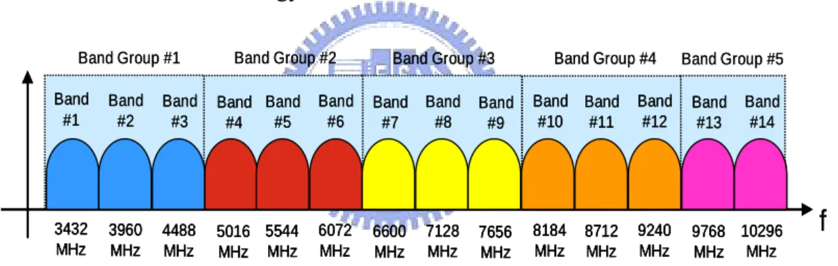
Band #1 Band #2 Band #3 Band #4 Band #5 Band #6 Band #7 Band #8 Band #9 Band #10 Band #11 Band #12 Band #13 Band #14 Band Group #1 Band Group #2 Band Group #3 Band Group #4 Band Group #5
3432 MHz 3960 MHz 4488 MHz 5016 MHz 5544 MHz 6072 MHz 6600 MHz 7128 MHz 7656 MHz 8184 MHz 8712 MHz 9240 MHz 9768 MHz 10296 MHz
f
Band #1 Band #2 Band #3 Band #4 Band #5 Band #6 Band #7 Band #8 Band #9 Band #10 Band #11 Band #12 Band #13 Band #14 Band #1 Band #2 Band #3 Band #4 Band #5 Band #6 Band #7 Band #8 Band #9 Band #10 Band #11 Band #12 Band #13 Band #14 Band Group #1 Band Group #2 Band Group #3 Band Group #4 Band Group #53432 MHz 3960 MHz 4488 MHz 5016 MHz 5544 MHz 6072 MHz 6600 MHz 7128 MHz 7656 MHz 8184 MHz 8712 MHz 9240 MHz 9768 MHz 10296 MHz 3432 MHz 3960 MHz 4488 MHz 5016 MHz 5544 MHz 6072 MHz 6600 MHz 7128 MHz 7656 MHz 8184 MHz 8712 MHz 9240 MHz 9768 MHz 10296 MHz
f
Figure 1.2 The direct-conversion architecture for UWB transceiver
One of the advantages of direct-conversion architecture for receivers (in Figure1.2) is that there is no image problem, and it does not require an image-reject filter. This is because the frequency of the RF signal is exactly equal to the frequency of the LO signal. However direct-conversion receivers have some issues which should be mitigated carefully, such as DC offsets, I/Q mismatch, even-order distortion, and flicker noise. In order to achieve the goal of the RF-SOC, we choose the direct-conversion architecture to design the system.
The frequency synthesizer must provide a clean and stable LO tone. The frequency band is from 3.1GHz to 10.6GHz and the frequency switching time is 9.5ns which is very difficult to achieve with traditional synthesizers with only one phased-lock loop
mixers, LC filters to achieve such short hopping time. In addition, UWB technology occupies such wide frequency range and any spurious emission will be a serious interferer for other wireless systems nearby. Therefore to suppress the spurious signals generated from the frequency synthesizer is very important. The goal of the thesis is to design a frequency synthesizer with fast switching time, wide synthesis frequency bands and low spurious emission for UWB transceivers.
1.3 UWB WPAN Specifications
ECMA368 partitions the spectrum from 3 to 10 GHz into 528MHz bands and employs OFDM in each band to transmit data rates as high as 480Mb/s. The relationship between center frequency and band number is given by the following equation:
Band center frequency=2904+528*Nb, Nb=1…14(MHz) (1.1) The band allocation is summarized in Table 2.1.
Each band consists of 128 sub-carriers of 4.125MHz bandwidth. In contrast to IEEE 802.11a/g, MB-OFDM UWB employs only QPSK modulation in each sub-carrier. The system hops at the end of each OFDM symbol (every 312.5ns). The band switching must be in less than 9.47ns. It is difficult to synthesize frequency to different bands by changing the division of the divider in short time. In order to make hopping frequency
band is needed, change the input signal of the mixer allows fast switching to another band. In this way, a short switching time can be achieved.
Table 1.1 OFDM PHY band allocation
1.3.1
Phase Noise
To derive the phase noise specification of the frequency synthesizer, consider the following equation [2]: 2 10 ) 10 1 ( 10 180 noise rms = ⋅ 20 ⋅ + p10 + p10⋅ loop k f π (1.2) 2 10 ) 10 1 ( 180 ) noise rms ( log 20 10 10 + ⋅ + ⋅ ⋅ = p p loop f k π (1.3)
k is the in-band phase noise density (dBc/Hz), p is the peaking of k, floop is the loop bandwidth of the phase lock loop. The rms phase noise from 0 Hz up to infinity in
loop bandwidth is 300 kHz, in order to achieve the integrated phase noise below 3.5 degrees rms, the phase noise should below -82dBc/Hz. The result can be calculated via the following equation.
) / ( 06 . 82 2 10 ) 10 1 ( 300 180 ) 3.5 ( log 20 10 0 10 0 dBc Hz k k =− ⋅ + + ⋅ ⋅ = π (1.4)
We can see the phase noise specification is not hard to do in the UWB system, but the spurious specification is difficult to achieve in the UWB system.
1.3.2
Spurious Tones
To derive the spurious tones specification of the frequency synthesizer, consider the Table 1.2 from [1], we can use maximum tolerable interferer at the antenna to calculate. Microwave Oven Bluetooth & 802.15.1 Interferer 802.11b & 802.15.3 Interferer 802.11a Interferer 802.15.4 Interferer Front-end pre-select filter attenuation (dB) 35 35 35 30 35 Max. tolerable interfere power at the antenna(dBm) -7.3 -5.8 -5.8 -17 -7.1
Table 1.2 Interference and Susceptible Analysis
In the receive path, the SNR of the wanted signal is calculated by the following equation:
noise wnated P
P
SNR= − (1.5) )
( interfer spurs
wnated P P P SNR= − − (1.6) SNR P P
Pspurs(Δω)= wanted − interfer − (1.7) If we have front-end pre-select filter attenuation, the changes are as the following equations: filter erfer wanted spurs w P P SNR P P (Δ )= − int − + (1.8) For example, if the transceiver operates at band 1, and the data rate is 110Mb/s, the spurs specification at 1.032GHz can be calculated by the microwave. The minimum sensitivity of the receiver is -74.1dBm.The required SNR is 3.6dB.
) ( 4 . 35 35 6 . 3 3 . 7 1 . 74 ) 032 . 1 ( GHz dBc Pspurs =− + − + =− (1.9) The interferers may be mixed with the spurs of the LO signal and down-converted to baseband, corrupting the desired signal. In the UWB system, it is more difficult to meet the LO spurs specification than phase noise specification.
1.3.3
Switching Time
The switching time is different from the settling time. In the UWB
system, the time between two hopping frequency is 9.47ns. It is difficult to change the division of the divider to meet the requirement. Selectors and mixers can be used to change the synthesized frequency to different bands, and therefore the switching time can be less than 9.47ns.
The overall design specification of the frequency synthesizer for UWB standard is shown in Table 1.3. The power consumption is designed as small as possible.
Parameters Specification Frequency range Phase Noise 3432Mhz~10296Mhz <-82.06dBc/Hz@100-kHz Switching Time In-band spurs Out-band spurs(at2.5G) Out-band spurs(at5.2G) <9.47ns <-12.6dBc <-36.9dBc <-30.7dBc Supply Voltage 1.8 V
Process UMC 0.18-μm CMOS
Table 1.3 Overall design Specification of the frequency synthesizer.
1.4 Organization
This thesis describes the design of CMOS frequency synthesizer for ultra wideband wireless PAN applications. Chapter 1 introduces the motivation and the specifications of frequency synthesizer for the UWB WPAN applications. Chapter 2 discusses the state of the art and the frequency planning in this work. Chapter 3 presents the spurious suppressing techniques in the proposed UWB frequency synthesizer. Chapter 4 presents the linear model of the phase-locked loop in order to decide the loop bandwidth, the phase margin, the phase noise, and the settling time in short time. The design and implementations of the frequency synthesizer are described in Chapter 5, including the
voltage-controlled oscillator, the frequency dividers, the phase frequency detector, the charge pump, the loop filter, and the single-sideband mixer. The layout, the testing setup, and measurement results of the voltage-controlled oscillator are also presented. The phase frequency detectors are also presented and the phase frequency detector with charge pumps in the package version. Chapter 6 gives the conclusions and the future works.
Chapter 2
Frequency Planning
There are many kinds of methods to synthesize frequencies. Such as direct synthesizers, indirect synthesizers (phase-locked loop frequency synthesizers), and direct digital frequency synthesizers. Because the phase-locked loop frequency synthesizer is easy to synthesize high frequencies and consumes low power, it is the most popular method used in high frequency synthesizers. In order to easily integrate in low-cost CMOS process and operate at high frequencies, we choose phase-locked loop synthesizer. There are many kinds of PLL frequency synthesizers changing division to synthesize various frequencies, such as integer-N, and fractional-N frequency synthesizers. However the time to switch between different band frequencies within a band group should be less than 9.47ns. The fast switching time precludes the use of a standard phase-locked loop (PLL)-based frequency synthesizer. Some possible ways of the performing the frequency generation in a UWB device are discussed in this section.
2.1 Architecture of UWB Frequency
Synthesizer
In the UWB system, the frequency range is from 3.1-GHz to 10.6-GHz, and the carrier switching time must below 9.47ns. The specifications of the switching time and the spurs are difficult to meet. The frequency hopping time can not be satisfied with conventional PLL-based frequency synthesizers because the locking time of the phase-locked loop is several hundreds ns or severalμs. In order to fast switch between bands, one approach incorporates some phase-locked loops and some single sideband mixers to synthesize different frequencies that present all time. The other approach incorporates multiple PLLs to generate different frequencies presented all times. The frequency range of the UWB system is very large, and the range covers the wireless LAN standard such as 802.11a. The reciprocal mixing effect can occur easily and degrade the wanted signal. In order to coexistent with other bands in 3-GHz~8-GHz, the suppression of the spurious must be concentrated. There are several kinds of UWB frequency synthesizer architectures and will be introduced in the following section.
2.1.1 State of the art 1
[3]
In [3], the UWB synthesizer shown in Figure 2.1 is designed to operate in “mode 1” bands. The frequency bands of mode 1 are 3432 MHz, 3960 MHz, and 4488 MHz. The three frequencies are produced by three fixed-modulus phase-locked loops,
therefore avoiding SSB mixers. The SSB mixer must have a low harmonic distortion, and the phase and gain mismatch can introduce spurious at the output of the SSB mixer. The output is changed between three voltage-controlled oscillators by the selector; therefore it may be sensitive to inductor coupling and carrier leakage. The architecture needs a good layout to provide good isolation. When the numbers of bands increases, the architecture will require more phase-locked loops, and it will increase the production cost and consume more power.
PLL1
PLL2
PLL3
Selector
3432MHz/3960MHz/ 4488MHz 3432MHz 3960MHz 4488MHzFigure 2.1 One band with one PLL frequency synthesizer
2.1.2 State of the art 2
[2]
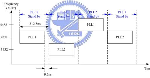
In [2], there are two phase-locked loops in the architecture as shown in Figure 2.3. In the UWB center frequencies, some high band frequencies are twice as larger as the low band frequencies. The 6864-MHz, 7392-MHz, and 7920-MHz frequencies are generated by a VCO in the PLL, and the 3432-MHz, 3960-MHz, and 4488-MHz
frequencies can be generated by divde-by-2 circuits. Therefore they can share the same phase-locked loop. For example, In Figure 2.2, when the frequency synthesizer is turned on, PLL1 provides the frequency to the present band (3960-MHz), and PLL2 is switched to the next band (3432-MHz). They operate by turns. Because the symbol period is 312.5ns, the settling time of the PLL standby must be less than 312.5ns. This means the architecture needs a wide loop bandwidth to achieve fast settling time, and the reference spurious problem will be critical. The charge pump circuit must be designed carefully because it is critical to minimize the reference spurious.
PLL1 PLL2 PLL1 PLL2 4488 3960 3432 Frequency (MHz) 312.5ns 9.5ns Time PLL2 Stand by PLL1 Stand by PLL2 Stand by PLL1 Stand by
Figure 2.3 Two phase-locked loops frequency synthesizer
2.1.3 State of the art 3
[4]
An approach to synthesize all bands needed by single-sideband mixers and phase-locked loops is introduced in the following sections.
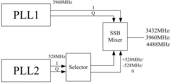
In [4], the architecture in Figure 2.4 uses two phase-locked loops to generate 3960-MHz and 528-MHz frequencies, then the single-sideband mixer spans the frequencies in band group one. Because the SSB mixer needs quadrature inputs, the quadrature signals are provided by the frequency divider circuit in the PLL. For example, in PLL1, it needs to provide quadrature signals at 3960MHz. Therefore the voltage-controlled oscillator needs to oscillate at 7920MHz, and the following divide-by-2 circuit (current mode logic architecture) can provide quadrature outputs at 3960MHz easily. The disadvantage is the spurs problem at the SSB mixer output.
SSB Mixer 3432MHz/ 3960MHz/ 4488MHz Selector I Q I Q 3960MHz +528MHz/ -528MHz/ 0 528MHz
Figure 2.4 Two phase-locked loops and one SSB mixer frequency synthesizer
2.1.4 State of the art 4
[5]
In [5], two PLLs are used again, but in a different way to generate seven bands from 3-GHz to 8-GHz. In Figure 2.5, one phase-locked loop provides two frequencies for input signals of the output SSB mixer. And the programmable tri-mode divider placed in front of the SSB mixer has a DC, and quadrature signalswith opposite I/Q sequences, therefore can provide more input signals for the SSB mixer. The SSB mixer has more selections of the input path. Therefore the frequences which the SSB mixer can synthesize will be more than the architecture in Figure 2.5. In order to suppress the spurious, the SSB mixer incorporates LC loads. The LC load acts as a band pass filter, and band switching is accomplished by using capacitor arrays to change the resonance frequency of the LC tank.
Figure 2.5 New two phase-locked loops and one SSB mixer frequency synthesizer
2.1.5 State of the art 5
[6]
In this year, a frequency synthesizer that generates twelve bands form 3.1-GHz to 9.5-GHz was presented. The frequency synthesizer consist SSB mixers and only one PLL. All the LO frequencies required for 3.1-GHz to 9.5-GHz operation are generated from the 8.448-GHz QVCO which consumes low power. A harmonic suppressing filter is inserted at the SSB1 mixer output terminal. The cut-off frequency of the filter is programmed according to the changing bands.
There are many kinds of architectures to implement the UWB frequency synthesizer. If the synthesizer architecture does not employ mixers, it required multiple PLLs, and therefore area and power consumption will be increased. The spurious problem is not serious because there is no mixer in the architecture. When the architecture applied to more bands, the carrier leakage problem will be more serious. If the synthesizer architecture consists of mixers, it required less PLLs, the area and power consumption are saved but more spurious will be introduced. The trade off must be made carefully to achieve fast switching time while not to increase area or power and to keep spurious minimized. In Table 2.1, the architecture consisting of mixers can synthesize more band frequencies and consume less power, but the spurious is higher than architecture without using mixers.
2005 JSSC PLL*2 7 3.4~7.9 1.8 1M -109.6 -52 116.28 0.18 CMOS [2] 2006 ISSCC PLL+SSB*2 12 3.4~9.2 1.1 1M -98 -20 47 0.09 CMOS [6] 2005 ISSCC PLL*2+SSB 3 3.4~4.5 2.7 1M -104 -35 27 0.25 SiGe [4] 2005 ISSCC PLL*2+SSB 7 3.4~7.9 2.2 1M -103 -37 48 0.18 CMOS [5] PLL*3 Architecture 3 No. of bands 2005 JSSC 3.4~4.5 1.5 1M -105 -60(only one on) 45 0.13 CMOS [3] Year Frequency range (GHz) Supply voltage (V) @Offset (Hz) Phase noise (dBc/Hz) Spurious (dBc) power (mW) Process (μm) 2005 JSSC PLL*2 7 3.4~7.9 1.8 1M -109.6 -52 116.28 0.18 CMOS [2] 2006 ISSCC PLL+SSB*2 12 3.4~9.2 1.1 1M -98 -20 47 0.09 CMOS [6] 2005 ISSCC PLL*2+SSB 3 3.4~4.5 2.7 1M -104 -35 27 0.25 SiGe [4] 2005 ISSCC PLL*2+SSB 7 3.4~7.9 2.2 1M -103 -37 48 0.18 CMOS [5] PLL*3 Architecture 3 No. of bands 2005 JSSC 3.4~4.5 1.5 1M -105 -60(only one on) 45 0.13 CMOS [3] Year Frequency range (GHz) Supply voltage (V) @Offset (Hz) Phase noise (dBc/Hz) Spurious (dBc) power (mW) Process (μm)
2.2 Frequency Planning
In order to synthesize all band group of the UWB system, there are more intermediate frequency components generated, and more SSB mixers are required. Therefore, the unwanted sidebands are accumulated through multi-stage mixing. The output signal will be degraded because of the multi-stage mixing. So the synthesizer must have approaches to suppress spurious signal. For example, the SSB mixer incorporates band-pass loads to suppress sidebands and spurious sinals.
Because the switching time is 9.47ns, and in order to design a UWB frequency synthesizer which can synthesize all band group frequencies, SSB mixers should be used or it will be difficult to synthesize all band group frequencies with less PLLs. Using multiple PLLs will consume much power and die area. And the LO leakage problem will be worse. So the architecture consisting of SSB mixers is used. In order to reduce the number of phase-locked loops and have a lot of auxiliary frequencies provided for SSB mixers, the frequency of the voltage-controlled oscillator must be chosen carefully. Some possible approaches of the frequency generation in a UWB are discussed in [7]. To generate all band groups, there will be a lot of intermediate frequencies provided for SSB mixers. The intermediate frequencies can be provided by the dividers in the phase-locked loop or the mixers. Using the divider is better because quadrature outputs are easily obtained and no need for power and area wasting mixer
components. In order to have maximum possible intermediate frequencies from a fixed VCO frequency, the division ratio should be with small size such as 2 and 3.
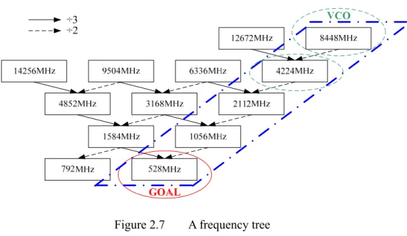
528-MHz is the baseband clock signal in MB-OFDM UWB system. In Figure 2.7, the frequency tree shows the different possible VCO frequencies that can generate a 528-MHz tone by successive division by 2, 3, or both. The SSB mixer requires quadrature signal inputs, and the quadrature signals can be generated by the passive RC polyphase filters or current mode logics. It is not practical by using polyphase filters, because multiple ployphase filters are required to cover all band groups and cost a lot of area. Aside from the problem, at high frequencies, the parasitic capacitances of the resistor are likely to make unacceptable errors in quadrature. In order to generate quadrature frequencies, the reliable way is by restricting all frequency division in the frequency synthesizer to current mode logic which can produce balanced quadrature outputs.
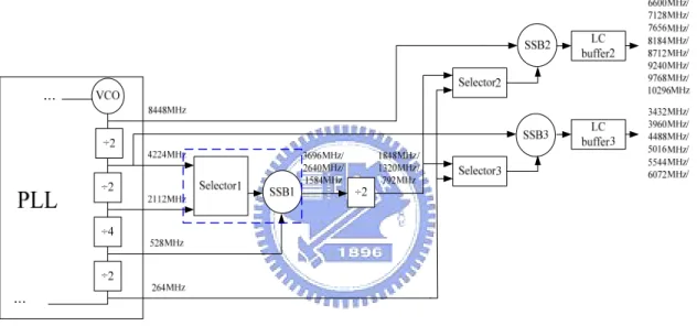
To sum up, in order to have more balanced quadrature intermediate frequencies by the phase-locked loop, choosing the VCO frequency as 8448-MHz and following the path enclosed by the dotted line (in Figure 2.7) is used in the proposed synthesizer design.
Figure 2.7 A frequency tree
The integer-N architecture is chosen in our phase-locked loop. Since the output signals of the frequency dividers are provided for SSB mixers, so they must be a fixed frequency values. The PLL can generate 8448-MHz and 4224-MHz frequencies. From
[1], 8448-MHz and 4224-MHz are upper frequencies of the 3960-MHz and 8184-MHz channels. Now regard these two as the major frequencies and separate the UWB center frequencies into two parts as shown in Figure.2.8. One part is close to 4224-MHz and the other is close to 8448-MHz. In order to synthesize all band group frequencies, the offset frequencies such as 264, 792, 1320, and 1848-MHz are required.
8448MHz 4224MHz 3432MHz 3960MHz 4488MHz 5016MHz 5544MHz 6072MHz 7128MHz 7656MHz 8184MHz 8712MHz 9240MHz 9768MHz 6600MHz 10296MHz 264MHz 792MHz 1320MHz 1848MHz Offset frequency
Major frequency Major frequency
Figure 2.8 Two parts of the UWB frequency bands
Instead of direct mixing these frequencies, a divide-by-two circuit is inserted after the mixer because the division helps to suppress spurious signals [9]. In order to insert a divide-by-two circuit after the mixer, the offset frequencies must be doubled. Therefore 528, 1584, 2640, and 3696 MHz at the mixer output are required and 528 MHz is already generated in the PLL. Now the intermediate frequencies in the PLL are used to generate the doubled offset frequencies. The mixer output frequency 1584 MHz is generated by down-converting 2112 MHz with 528 MHz. (Note: both 2112 MHz and 528 MHz are generated in the PLL). In the similar way, 2640 and 3696 MHz can be acquired by up-converting 2112 MHz with 528 MHz and by down-converting 4224
MHz with 528 MHz respectively. In Fig. 3, the PLL can generate frequencies of 8448, 4224, 2112, 528, and 264 MHz. The SSB1 mixer output frequency is 1584, 2640, or 3696 MHz, and the offset frequencies can be acquired after the divider following the SSB1 mixer. Hence, the SSB2 mixer and the SSB3 mixer can generate all band group frequencies for UWB systems by the major frequencies (8448 and 4224 MHz) and the offset frequencies (264, 792, 1320, and 1848 MHz).
Chapter 3
Spurious Suppressing Techniques
Frequency spurious of the LO signal can down-convert in-band signals to the same frequency as the wanted band. To meet the specification on low LO spurs is much more difficult than the specification on low phase noise in the UWB system. Therefore to decrease the spurious in the UWB system is very important. This chapter will introduce some spurious suppressing techniques in this work.
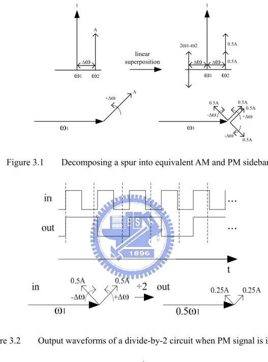
3.1 Using Divide-By-2 Circuit After the Mixer
Literature [9], presented that the spurs after division-by-2 is lower than spurs before division-by-2. In Figure 3.1, consider two tones atω
1 andω
2 applied to the divide-by-2 circuit.ω
1 is the wanted signal andω
2 is the unwanted spurious whose amplitude is A. The spurious toneω
2=ω
1+Δω
can be decomposed into equal amplitude modulation (AM) and phase modulated (PM) sidebands by linear superposition. Each of them is the same amplitude A/2, and they locate symmetricallyΔω
away fromω
1.The flip-flop (the divide-by-2 circuit) is sensitive only to the threshold crossing of the input signals. (Note: Assume the differential threshold is zero) Therefore, the flip
flop only reacts to the input PM signals.
In Figure 3.2, the input PM signal is applied to the flip-flop. Whenever the differential clock input across zero, the flip-flop output toggles. The appearance is clear in the time-domain input and output waveforms. The output waveform tracks the input waveform whenever the input signal is at positive-slop trigger. The deviation is also tracked by the flip flop. However, the output frequency is half of the input frequency; the deviation in phase at output is half corresponding to the input signal. Therefore, the PM sidebands at output are half of the input PM sidebands at input. So the amplitude of the output PM sidebands are 0.25A. However, the rate or relative frequency of PM is still the same as before. Therefore, the sidebands are located at ω ±Δω
2
1 .
To sum up, when large interesting input tones and small unwanted input spurs are applied to the to the divede-by-2 circuit, the large interesting input tones are divided by two, and each of the small unwanted input spurs is surrounded by two output spurs that are symmetrically disposed around the large tone at the same frequency offset as the single input spur but at 1/4 (-12 dB) the input spur’s relation amplitude. (In Figure 3.3) More frequency division-by-2 conserves the spur separation but lowers the relative levels by 6 dB.
In an SSB mixer followed by frequency division, gain mismatch and phase errors in the I and Q mixers will generate a small unwanted spurs. This is the input of the
divider From above discussing, the divide-by-two circuit can help to suppress spurious. +Δω ω1 ω1 ω2 1 A Δω ω1 ω2 0.5A 2ω1-ω2 -Δω 0.5A 0.5A ω1 -Δω +Δω 0.5A 0.5A 1 Δω 0.5A Δω A linear superposition
Figure 3.1 Decomposing a spur into equivalent AM and PM sidebands
Figure 3.2 Output waveforms of a divide-by-2 circuit when PM signal is input
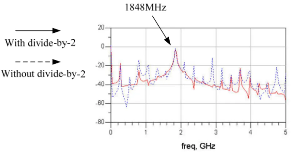
Figure 3.4, 3.5, and 3.6 respectively show the output spectrums of the 792-MHz, 1320-MHz, and 1848-MHz generated with and without the divide-by-two circuit. The dot line presents the output without divide-by-two circuit, and the solid line is for that with dive-by-two circuit.
Since the input frequencies of the mixer with and without divide-by-2 are different, the spurs at output are not at the same offset frequency away from carrier frequencies. But the spurious near the synthesized frequency with divide-by-two circuit is lower than that without divide-by-two circuit.
Figure 3.4 Frequency spectrums of 794-MHz
Figure 3.6 Frequency spectrums of 1848-MHz
3.2 Single-Sideband Mixer
Single-sideband mixers are employed in the proposed synthesizer. As shown in Figure 3.7, the relation between the output and the input of the mixer is in the following equation. t t t t t
Out=cos(ω1 )cos(ω2 )±sin(ω1 )sin(ω2 )=cos(ω1 mω2) (3.1) Therefore, the architecture can make the unwanted sideband lower. But SSB mixers require quadrature inputs and arise two issues which are the mismatches between the quadrature inputs and the nonlinearities. A general way to quantifying the I/Q mismatch in a SSB mixer is to concern two signals V0sinω1t and V0cosω1t to the I
and Q inputs and check the spectrum produced by the adder. In the ideal case, the SSB mixer output is shown as equation 3.2. In equation 3.3, ε is a gain mismatch, and θ is phase imbalance. t V t t V t t V
) sin( ) sin( ) cos( ) cos( ) 1 ( 1 2 0 1 2 0 t t V t t V Out= +ε ω ω +θ + ω ω (3.3) t V t V
Out (1 )sin sin( )
2 ) cos( ] cos ) 1 ( 1 [ 20 + +ε θ ω1 −ω2 − 0 +ε θ ω2 −ω1 ≈ (3.4) t V t V ) sin( sin ) 1 ( 2 ) cos( ] cos ) 1 ( 1 [ 20 − + +ε θ ω1 +ω2 − 0 +ε θ ω2 +ω1 +
The power of the sideband at ω2 +ω1 divided by that of the sideband at
1
2 ω
ω − is in the following equation.
ε θ ε ε θ ε + + + + + − ≈ cos ) 1 ( 1 cos ) 1 ( 1 sub add P P (3.5) In practice, the cross-talk between the two data streams becomes negligible if the above test yields an unwanted sideband about 30dB below the wanted signal.
The mixers are usually designed such that the switching port experiences rapid switching. The switching port is so nonlinear that the RF signal is multiplied by a rectangular waveform. Therefore, in Figure 3.7, harmonics of
ω
1 andω
2 are generatedin each port of the mixers, leading to various cross-products after multiplication. The problem will be mitigated by using LC tank. We will introduce in the next section.
3.3 LC Tank with Switching Inductor
The SSB mixer in Figure3.8 incorporates band pass loads to suppress spurious [5]. The SSB mixer with inductor loads are used to achieve broadband operation. Band selection is accomplished by adding capacitor arrays to adjust the resonances frequency of the tanks. The wide range operation (3-8GHz) of [5] uses multiple LC tanks. In order to extend the frequency range of the SSB mixer, more LC tanks are required leading more area expansion. However, with some modification on the LC tank, the area can be kept while the operation bandwidth can be improved.
Figure 3.8 A SSB mixer with band pass loads
Changing the resonant frequency of the LC tanks is discussed in [10]. The maximum Q attainable is dominated by the on-chip inductor Q in low-cost CMOS process. Therefore, a restricted bandwidth is obtained at high frequency, and that is not enough for wideband applications. An easy way to raise the bandwidth is to decrease the
For LC tanks, the center frequency can be tuned either by inductors or capacitors. The most commonly used approach is to vary the parallel capacitors either by varactors or switched-capacitor arrays. However, since the tank impedance would be degraded with the increased capacitance, the tank impedance is lower at lower frequencies as compared to that at higher frequencies. As a result, either the output swing or the power consumption would need to be compromised.
As a better choice to varying the parallel capacitors, the tank inductance can be varied by employing MOS with the center taped inductors. As shown in Figure 3.9, there is a PMOS switch on the center of the inductor. When the voltage Vc is VDD, the PMOS switch is open, and the effective inductance is L. On the other side, when the voltage Vc is GND, the PMOS switch is turned on, and the effective inductance is about L/2.
Figure 3.9 A switching inductor
We can use switching inductors to change the resonance frequencies of the LC tanks. In this way, we can avoid using large capacitance, and acquire higher impedance
and wider operation bandwidth.
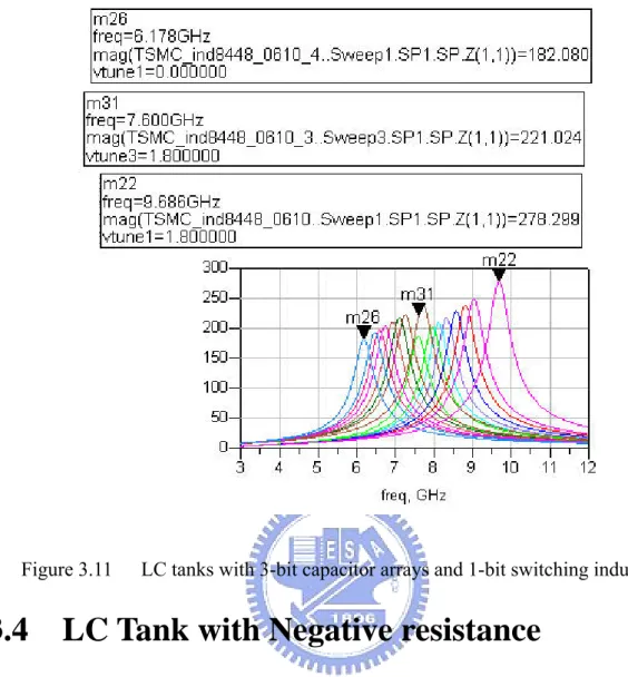
Figure 3.10 shows the impedance of the LC tank with 5-bit capacitor arrays, while Figure 3.11 is the impedance of the LC tank with 3-bit capacitor arrays and 1-bit switching inductor. It is apparent that using switching inductor can operate wider frequency range and have higher and flat impedance.
Figure 3.11 LC tanks with 3-bit capacitor arrays and 1-bit switching inductor
3.4 LC Tank with Negative resistance
To have a band-pass load which can operate all band groups in the UWB system requires a lot of capacitance arrays to change the resonance frequency More capacitance also means more parasitic resistances which degrade the quality factor of the LC tank. In order to have a high quality factor, a negative resistance is put in parallel in the LC tank. The architecture is shown in Figure 3.12. The negative resistance can compensate the parasitic resistance and increase the quality factor.
VT2 VT1 VT0 VT0 VT1 VT2
-R
Figure 3.12 LC tanks with a negative resistance
Figure 3.13 and 3.14 show the impedance of the LC tank without and with negative resistance respectively. With the negative resistance, the resonant impedance is much higher.
Figure 3.14 LC tanks with negative resistance
Figure 3.15, 3.16 show the output spectrums respectively when the frequency band is at 4488-MHz, 8712-MHz.
The circle solid line is the output spectrum of the last stage mixer. (SSB1 or SSB2 mixer in Figure 2.9) The star solid line and the solid line are the output spectrums of the LC buffer without and with negative resistance respectively. In Figure 3.15, spurious is suppressed 6.697dB more with using negative resistance than without using negative resistance, when the frequency band is at 4488-MHz. Similarly, when the frequency band is at 8712-MHz, it improves 7.152dB.
Figure 3.15 Output spectrums at 4488-MHz
Chapter 4
Frequency Synthesizer Design
4.1 Modeling of the PLL
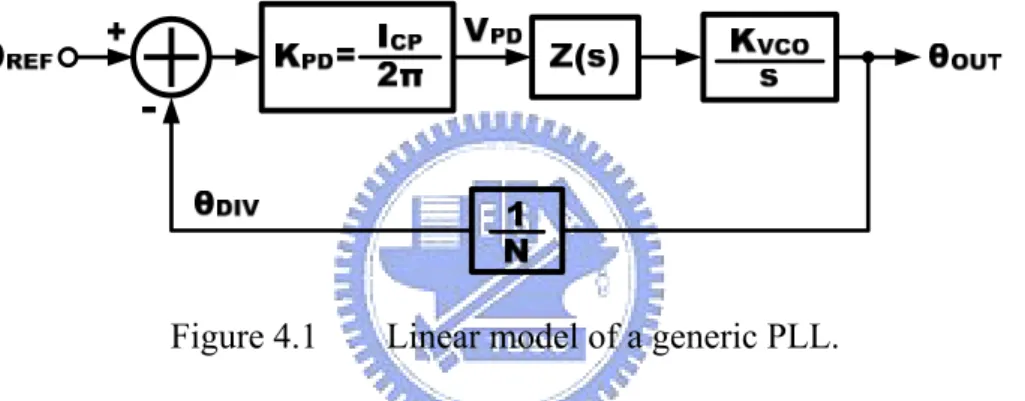
Figure 4.1 is a linear model of a phase-locked loop. The model can help to evaluate the performance of the PLL, such as phase noise, loop stability, and settling time.
Figure 4.1 Linear model of a generic PLL.
The phase detector can generate a dc value proportional to the phase difference between the input reference signal θREF and the divided signal θDIV.. KPD is the phase
detector gain in V/rad. The phase detector can be modeled as a substrator. Therefore, the output signal of the phase detector can be expressed by the following equation.
) ( REF DIV
PD
PD K
V = θ −θ (4.1) Although the phase detector gain KPD is nonlinear, the transfer characteristic of the
phase detector can be regarded as linear in its operating region. The phase error signal VPD is filtered by the low pass loop filter. which is expressed by Z(s). For example, a
(
)
(
)
z i p 1 + s Z(s) = sC 1 + sτ
τ
⋅ (4.2)The capacitance Ci contributes a pole at origin, τZ is a zero for stability concern,
and τP is a pole for high-frequency spurs filtering.
The output frequency of the VCO is controlled by the voltage VCONT. The relation
between the changing frequency of the VCO and the control voltage is Δω=KVCO·VCONT.
KVCO is the VCO gain (specified in rad/s/V) and it is nonlinear. Since frequency is
derivative of phase, the VCO can be modeled by the following equation.
s s V K s VCO CONT OUT ) ( ) ( = ⋅ θ (4.3) Because frequency and phase are related by a linear operator, the division of frequency by a factor N is the same to the division of phase by the same factor. Hence, the frequency divider can be modeled by the following equation.
N
OUT DIV
θ
θ = (4.4) Based on the linear model of the PLL, the open loop transfer function can be expressed as follows: ( ) 1 ( ) ( ) KPD Z s KVCO G s H s N s ⋅ ⋅ = ⋅ (4.5) This transfer function can estimate the performance of the PLL.
4.1.1 Loop Stability
In Figure 4.1, because the phased-locked loop in this work employs the charge-pump circuit, the phase detector gain is determined by the charge pump output
current (KPD=ICP/2π).
The second order passive loop filter shown in Figure 4.2 consists of a capacitor CZ
for zero phase error, a resistor RZ for stability consideration, and a capacitor CP for
high-frequency spurs filtering.
Figure 4.2 A second order passive loop filter. The impedance of the second order passive loop filter is expressed as
) 1 ( ) 1 ( ] 1 //[ 1 ) ( p z P z p z z P C s s s sC R sC s Z τ τ τ τ + + = + = (4.6)
The time constants τZ and τP are given by equation (4.7) and (4.8)
z= R Cz z
τ
⋅ (4.7) z p p z z p C C = R C + Cτ
⋅ (4.8)The time constants determine the pole and zero frequencies of the loop filter. The open loop transfer function of the system can be expressed as the following equation.
(
)
(
)
PD VCO p z 2 p z p K K 1 + s G(s) H(s) = s C N 1 + sτ
τ
τ
τ
⋅ ⋅ ⋅ ⋅ ⋅ ⋅ ⋅ ⋅ (4.9)(
)
(
)
PD VCO p z 2 p z p K K 1 + jω G(j ) H(j ) = -ω C N 1 + jωτ
τ
τ
τ
ω ⋅ ω ⋅ ⋅ ⋅ ⋅ ⋅ ⋅ ⋅ (4.10)) ( tan ) ( tan 180 ) ( 1 1 p z ω τ τ ω ω ϕ =− + − ⋅ − − ⋅ (4.11) ) ( tan ) ( tan ) 180 ( ) ( 1 1 p z PM =ϕ ω − − = − ω⋅τ − − ω⋅τ (4.12)
The Bode plot of the open loop response is shown in Figure 4.3 where the loop bandwidth, ωu, is defined as the corresponding frequency when the magnitude of the
open loop gain equals one (i.e., unity-gain frequency). The phase margin is chosen between 50o and 70o.
Figure 4.3 Open loop response bode plot.
By setting the derivative of the phase margin equal to zero, the frequency with the maximum phase margin is found, and it is expressed in terms of zero and pole as equation (4.14) z p 2 2 z p d (ω) = - = 0 dω 1 + (ω ) 1 + (ω )
φ
τ
τ
τ
τ
⋅ ⋅ (4.13) u z p z p 1 ω = = ω ωτ τ
⋅ ⋅ (4.14)PD VCO p z 2 u u p z u p 1 + j K K G(s) H(s) = = 1 N 1 ω C ω j ω +
τ
τ
τ
τ
⋅ ⋅ ⋅ ⋅ ⋅ ⋅ ⋅ (4.15) 2 PD VCO p u z p 2 2 p z u u p 1 + (ω ) K K C = ω C N 1 + (ω )τ
τ
τ
τ
⋅ ⋅ ⋅ ⋅ ⋅ ⋅ (4.16) The time constants, τZ and τP are expressed in terms of phase margin and loopbandwidth as follows p u secPM - tanPM = ω
τ
(4.17) z 2 u p 1 = ωτ
τ
⋅ (4.18) The component values of the second order filter are2 2 2 1 ( ) ) ( 1 p u z u z u p VCO PD P N K K C τ ω τ ω τ ω τ + + ⋅ ⋅ ⋅ ⋅ = (4.19) z z p p C = C (
τ
- 1)τ
⋅ (4.20) z z z R = Cτ
(4.21) Table 4.1 summarizes the loop parameters of the phase-locked loop The VCO gain is 280 MHz/V. The charge pump current is about 210 μA. In this work, the loop bandwidth and the phase margin are chosen to be 300-kHz and 60 o respectively. The values of the loop filter components are RZ = 8.84 kΩ, CZ = 224 pF, and CP = 17.32 pF.The KVCO of the VCO is from 180MHz/V to 450MHz/V. When Kvco is 180MHz/V,
300MHz/V, and 450MHz/V, the phase margins are 50 degrees, 60 degrees, 40 degrees. All of the phase margins are lower than 40 degrees.
Parameters Value
Loop Bandwidth ωu 300-kHz
Phase Margin φP 60o
VCO Gain KVCO 280 MHz/V
Charge Pump Current ICP 210 μA
RZ 8.84 kΩ
CZ 224 pF
CP 17.32 pF
Table 4.1 Summary of loop parameters.
4.1.2 Noise Characteristic of the PLL
In the PLL, there are two main noise sources which are from VCO and reference signals. The transfer function of the noise source from the VCO output is a high-pass characteristic. In the same way, the transfer function of the noise source from the reference clock input is a low-pass characteristic. That one or both noise sources are significant depends on the application of the phase-locked loop. Therefore, the optimum choice of the loop bandwidth in the PLL is important. In the wireless frequency synthesizer, due to the high quality of the crystal-based reference signal, the VCO phase noise dominates the noise. Therefore, it is desirable to make the loop bandwidth wider
Since the input reference of the phase-locked loop is crystal-based, phase noise contributions from the reference and frequency dividers are very low and negligible. Consider the phase noise contribution from the VCO, charge pump, and loop filter. The transfer function from noise sources to the output can be obtained by the linear PLL model. To derive the transfer function, the linear model of the PLL is shown in Figure 4.4.
Figure 4.4 Linear model of the PLL with noise source
The transfer function from the input phase θin to the output phase θout can be
expressed as the following equation, and is a low-pass function.
(4.22)
Therefore, the phase noise of the reference is attenuated at large frequency offset. (Note: The close-in phase noise of the reference signals is also amplified by the division ratio N of the divider)
The transfer function from the VCO noise θn,VCO to the output phase θout can be
expressed as the following equation, and is a high-pass function. s N K s Z K s K s Z K VCO PD VCO PD in out ⋅ ⋅ ⋅ + ⋅ ⋅ = ) ( 1 ) ( θ θ
(4.23)
Hence, the far-offset phase noise of the PLL is dominated by the VCO phase noise. The transfer function from the charge pump noise current In,CP to the output phase
θout can be expressed as the following equation, and is a low-pass function.
(4.24)
In the design of the loop filter, phase noise contribution due to the thermal noise of Rz is also an important issue. The transfer function can also be derived as the following
equation, and is a band-pass function.
(4.25)
It is desirable to reduce the value of Rz and increase the value of Cz at the cost of
large chip area for on-chip components.
4.1.3 Behavior Simulation of the PLL
The behavior and circuit (transistor level) simulations are performed in Advanced Design System (ADS). To verify the design of the loop filter in the previous section, the magnitude and phase response of both the open and closed loop are shown in Figure 4.5 where the loop bandwidth and phase margin of the phase-locked loop are 300-kHz and
s N K s Z KPD VCO vco out ⋅ ⋅ ⋅ + = ) ( 1 1 θ θ s N K s Z K s K s Z I PD VCO VCO CP n out ⋅ ⋅ ⋅ + ⋅ = ) ( 1 ) ( , θ s N K s Z K s K V PD VCO VCO R n out ⋅ ⋅ ⋅ + = ) ( 1 , θ
60o, respectively.
Figure 4.5 Magnitude and phase response of the open and closed loop.
In the UWB system, the switching time is 9.47ns, and it is difficult to meet with traditional PLL-based synthesizer. In order to achieve fast switching time, mixers are employed in the synthesizers. Therefore, the settling time of the PLL does not need to be very fast. The behavior simulation of the PLL can help to check whether the PLL is locked or not. Figure 4.6 is the PLL simulation in time domain.
Figure 4.6 Settling time of the phase-locked loop
The simulated loop reductions of the VCO phase noise is shown in Figure 4.7. Since the transfer function from the VCO phase noise to the output phase noise
indicated in Equation (4.22) is a high-pass characteristic. The VCO phase noise is suppressed with the bandwidth of the loop. And the far-offset phase noise of the PLL is dominated by the VCO phase noise. On the other side, the short-offset phase noise of the PLL is dominated by the reference phase noise.
Figure 4.7 Simulated loop reductions of the VCO phase noise.
4.2 Circuit Design
4.2.1 Voltage-Controlled Oscillator
The voltage-controlled oscillator (VCO) is the most important building block of the frequency synthesizer. The design considerations are phase noise, tuning range, frequency pushing, frequency pulling, output power, and power consumption.
There are many kinds of oscillators, such as ring oscillators and LC oscillators. LC oscillators are the best choice for the wireless applications, because ring oscillators suffer from worse phase noise performance.
4.2.1.1
Phase Noise Theory
Figure 4.8 Leeson’s phase noise model.
The model can be expressed in the following equation. (Note: Psig is the signal
power. Q is the quality factor of LC tank. F is an empirical factor to predict the increased noise in the 1/(Δω)2 region. Δω1/f3 is the corner frequency between 1/(Δω)2 region and 1/(Δω)3 region)
3 2 1/ 0 2 { } 10log {1 } 1 2 f sig FkT L P Q ω ω ω ω ω ⎡ ⎛ ⎞ ⎛ Δ ⎞⎤ Δ = ⎢ +⎜ ⎟ ⎜⎜ + ⎟⎟⎥ Δ Δ ⎢ ⎝ ⎠ ⎝ ⎠⎥ ⎣ ⎦ (4.26)
The Leeson’s phase noise model shows that increasing the signal amplitude and quality factor of resonator can reduce phase noise.
The basic model [12] is shown in Figure 4.9 which can help to predict the phase noise. (Rp is the parasitic resistance. I is the current noise source of RR2P p Gm is an
Figure 4.9 Basic model of oscillator circuit. The transfer function from the current noise source
P
2 R
I to the output voltage Vout
can be derived and expressed as the following equation.
(4.27) Gp is the inverse of Rp. Hnoise(ω) is the inverse of the noise transfer function.
Consider the noise transfer function at a frequency offset ω0+Δω, Hnoise(ω) can be
expressed by Taylor series expansion around the center frequency.
(4.28) The first term Hnoise,Rp(ω ) is equal to zero and the second term is equal to o
p p noise,R o noise,R o o o o dH (ω ) dH (ω ) Δω C Δω Δω = ω = 2j dω dω ω L ω ⎛ ⎞ ⎛ ⎞ ⋅ ⋅ ⋅⎜ ⎟ ⋅ ⋅⎜ ⎟ ⎝ ⎠ ⎝ ⎠ (4.29)
Then, the noise transfer function is given by
(
)
p 2 2 2 2 o o noise,R 2 o ω ω 1 L 1 T (s) 2j C Δω 4 ω C Δω ⎛ ⎞ ⎛ ⎞ ≈ ⋅ ⋅⎜ ⎟ = ⋅⎜ ⎟ ⎝ ⎠ ⋅ ⎝ ⎠ (4.30)The noise density at a frequency offset ω0+Δω is given by
(4.31) 2 2 2 2 2 ) ) ( 1 ( ) ( ) ( LC s G G s sL s I V s T P M Rp out noise = = − − + ω ω ω ω ω ω ω ω ≈ + Δ Δ + = Δ + d dH H T H noise o o noise o noise o noise ) ( ) ( ) ( 1 ) ( f C Rp kT I T V o o Rp noise Rp out +Δ = +Δ ⋅ ≈ ⋅ Δ ⋅Δ 2 2 2 0 2 0 2 , ( ) ) ( 1 ) ( ) ( ω ω ω ω ω ω ω
given by p M,R p 1 G = R (4.32) The noise can be split up into a amplitude modulation (AM) and a phase modulation (PM). Therefore, the phase noise is typically half the value given by Equation (4.31).
The noise generated by inductor series resistance Rl and capacitor series resistance
Rc can also be calculated. (Note: Series resistances must transfer to parallel resistances
by the quality factor) The noise contribution of Rl and Rc can be expressed as follows
(4.33) (4.34) The power needed to maintain the oscillation in the existence of Rl or Rc are given
by
(
)
l 2 M,R l o G = R ω C (4.35)(
)
c 2 M,R c o G = R ω C (4.36) The effective resistance is then defined for the evaluation of the LC oscillators. And the phase noise due to the parasitic resistances can be summarized as follows(
)
eff c l 2 p o 1 R R R R ω C = + + (4.37)(
)
2 M eff o G = R ω C (4.38) (4.39) f Rl kT V o Rl out2, ( 0 +Δ )= ⋅ ⋅(Δω)2 ⋅Δ ω ω ω f R kT V o c Rc out2, ( 0 +Δ )= ⋅ ⋅(Δω)2⋅Δ ω ω ω f R kT f C Rp Rc Rl kT V o eff o o R vout +Δ = ⋅ + + ⋅ Δ ⋅Δ = ⋅ ⋅ Δ ⋅Δ 2 2 0 2 , ( )) ( ) ( ) 1 ( ) ( ω ω ω ω ω ω ωThe quality factor of the LC tank can also be expressed in terms of the effective resistance as follows 0 0 0 0 1 1 1 1 1 1 1 ( ) ( ) R ( ) ( ) p l c eff l c R R R p Q C R C R C Q Q Q R C ω ω ω ω = = = + + + + (4.40)
Similarly, the phase noise due to the active element can also be calculated. The current noise source of the active element is given by
2
n M
I = 4kT F G⋅ ⋅ ⋅Δf (4.41) where GM is given by Equation (4.38) and F is the noise factor of the amplifier.
Since the noise source of the active element is the same as the noise source of the parallel resistance Rp. The noise transfer function is also given by Equation (4.30).
Therefore, the phase noise due to the active element is expressed as follows
(
)
M p 2 2 2 2 o out,G noise,R n 2 M o ω 1 V (ω + Δω) = T (ω + Δω) I kT F G Δf Δω ω C ⎛ ⎞ × ≈ ⋅ ⋅ ⋅ ⋅⎜ ⎟ ⋅ ⎝ ⎠ (4.42) (4.43)In the design of an actual oscillator, the transconductance used in the circuit will be higher than theoretically needed. The transconductance must be higher than Reff to
provide enough negative resistance. By multiplying the noise with a factor α in the equations, the amount of noise which the actual amplifier generates in excess of the ideal amplifier is included. Define a factor A equal to α · F, Equation (4.43) becomes as follows f F R kT V o eff G out M +Δ = ⋅ ⋅ ⋅ Δ ⋅Δ 2 2 , ( ) ( ω) ω ω ω