Influences of template layer thickness on strain fields and transition
energies in self-assembled SiGe/ Si quantum dots
M. K. Kuo,a兲 T. R. Lin, and K. B. Hong
Institute of Applied Mechanics, National Taiwan University, No. 1 Sec. 4 Roosevelt Road, Taipei, 10672 Taiwan
共Received 25 May 2007; accepted 7 January 2008; published online 2 April 2008兲
This paper investigates the influence of thickness of template layer on strain fields and transition energies in lens-shaped self-assembled SiGe/Si quantum dots. This study analyzes strain fields in and around quantum dots on the basis of the theory of linear elasticity. Strain fields are then incorporated into the steady-state effective-mass Schrödinger equation. Energy levels and wavefunctions of both electrons and holes are calculated. The calculated results of strain-induced phonon frequency are consistent with previous results obtained by Raman spectroscopy. Moreover, the calculated transition energy agrees well with previous experimental photoluminescence data. Numerical results also suggest that transition energy decreases as the template layer thickness increases. © 2008 American Institute of Physics.关DOI:10.1063/1.2891418兴
I. INTRODUCTION
Due to three-dimensional quantum confinements, quan-tum dots 共QDs兲 possess several interesting characteristics, including discrete energy levels and “atomlike” electronic states. These characteristics and their potential applications in optoelectronics have recently attracted substantial atten-tion in the investigaatten-tion of QDs.1,2 Numerous studies have reported on InGaAs/GaAs and other group III-V quantum-dot heterostructures showing a wide range of quantum-dot sizes and shapes.2–4Group IV quantum-dot systems, such as SiGe/Si, are also interesting because of their potential applications in devices and their compatibility with silicon-based technology.5–7
Strain fields in and around self-assembled quantum dots 共SAQDs兲 strongly affect optoelectronic properties of QDs. Hydrostatic strain shifts the edges of the conduction and the valence bands, while the uniaxial strain lifts the band degen-eracy. Designing optoelectronic devices requires an accurate determination of the induced strain fields in both the quan-tum dot and the surrounding matrix. This information reveals how material parameters affect the conduction and valence bands and their curvatures, thereby altering the effective masses and transport properties.
Recently, Kurdi et al.8 evaluated the strain fields of SiGe/Si SAQDs using valence force field theory. Makeev and co-workers9,10 studied stress distribution in Ge/Si QDs using atomistic simulations. This paper investigates strain fields and energy levels in QDs using finite element method 共FEM兲 to simulate the system of SiGe/Si QDs. The FEM is a very versatile and effective numerical method for accom-modating different theories to model QDs at various levels of complexity. Previous studies4 using the FEM showed good agreement with experimental photoluminescence data. This study analyzes strain fields induced by lattice mismatches in heterostructures on the basis of the theory of linear elasticity. The three-dimensional steady-state Schrödinger equation is
then modified by incorporating the effects of strain fields into the carrier confinement potential and is analyzed by FEM numerically. The results include the energy levels and wave-function spectra of SiGe/Si QDs. The calculated strain fields are also used to evaluate the strain-induced phonon frequen-cies which, along with the calculated transition energies, are compared against experimental data. Finally, this paper dis-cusses the influence of template layer thickness on transition energies in SiGe/Si QDs.
II. PROBLEM STATEMENT
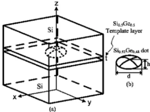
This paper considers a single lens-shaped SiGe QD bur-ied in a Si matrix, as depicted schematically in Fig.1. A thin template layer of Si0.5Ge0.5is first grown on a共001兲 Si sub-strate. A thin Ge layer is then deposited on the template layer. Spontaneous coherent island formation then produces SAQDs. Finally, the quantum-dot islands are covered by a further deposition of the same material as the substrate. Nu-merical examples in this paper consider three different thick-nesses of the Si0.5Ge0.5template layer: t = 3, 4, and 5 nm, all of which are less than the critical thickness.11 The base di-ameter d and height h of the quantum dot are 70 and 21 nm, respectively. The thicknesses of the substrate and the capping
a兲Electronic mail: [email protected]. FIG. 1.are the base diameter and height of the island, respectively.共a兲 Schematics and geometries of Ge QD nanostructure. 共b兲 d and h
layer are 80 and 60 nm, respectively. The SiGe QD is as-sumed to have a uniform Ge concentration of 48%.12
III. STRAIN FIELD
Epitaxially grown semiconductor structures often consist of materials with different lattice constants. The mismatch of lattice constants creates strain fields in quantum-dot hetero-structures, which affect the optoelectronic properties of quantum dots. In-plane lattice mismatch parameters13are de-fined as
共0兲xx=共0兲yy=
as− ad
ad
共1兲 where as and ad are the lattice constants of the substrate
共lower layer兲 and the quantum dots 共upper layer兲 materials, respectively. The numerical values of lattice constant of the Si1−cGec are set as 5.431+ 0.1992c + 0.02733c2, where c is
the Ge concentration.14 In this example, the lattice constant of the substrate material共Si兲 is smaller than that of the tem-plate layer material共Si0.5Ge0.5兲. However, the lattice constant of the template-layer material exceeds that of the quantum-dot material共Si0.52Ge0.48兲. Therefore, the Si layer compresses the Si0.5Ge0.5template layer, and the Si0.5Ge0.5template layer puts tension on the Si0.52Ge0.48 dot. In other words, the Si0.52Ge0.48 dot will be less compressive than the Si0.5Ge0.5 template layer.
This paper assumes the deposition material adjusts its in-plane lattice constant to that of the substrate during epi-taxial growth. It therefore induces an initial in-plane strain in the deposition material 关i.e., 共0兲xx= 共0兲yyin Eq. 共1兲兴. The
initial in-plane strain also accompanies an initial normal strain in the z axis共the direction of QD growth兲 in the depo-sition material due to Poisson’s effect.15,16 Based on the plane-stress assumption,17 the initial out-of-plane strain 共0兲zzleads to
共0兲zz= −
2C12
C11
共0兲xx. 共2兲
Here, both Si and Si1−cGecare considered as cubic materials.
Each material has three independent elastic moduli: C11, C12, and C44. The numerical values of elastic moduli used in this paper are taken from Ref.18.
Notice that the lattice mismatch parameters defined in Eq.共1兲are not yet the complete strain fields in the quantum-dot island. In fact, lattice mismatches will induce further elastic deformation in the entire nanostructure system, in the substrate, template layer, and the island, to ensure the equi-librium of the corresponding stresses. This paper regards the parameters 共0兲xx, 共0兲yy, and 共0兲zz as the initial normal
strains in the x-, y-, and z-directions, respectively. These ini-tial strains in the template layer and the island induce further elastic strain fields in the entire SAQD system. Therefore, they serve as inputs in the following finite element analysis. According to the theory of linear elasticity, the relation-ship between stressesij, total strainskl, and initial strains
can be expressed as
ij= Cijkl
关
kl− 共0兲kl兴
, i, j,k,l = x,y,z, 共3兲where Cijkl is the component of the fourth-order tensor of
elastic moduli and 共0兲kl denotes the initial strain tensors
described in Eqs.共1兲 and共2兲 with
共0兲kl= 0 for k⫽ l. 共4兲
This paper uses a finite element package 共COMSOL Mult-iphysics兲 to analyze the linear elastic boundary value prob-lem. This problem arises from the mismatch in lattice con-stants between the island, the template layer, and substrate materials. Analysis requires appropriate boundary conditions. The periodic symmetric argument requires that all nodes of the x- and y-outer surfaces are fixed against displacement in the normal direction. The bottom outer surface is fixed against displacement in the z-direction to avoid any possible rigid body translation. The upper surface is kept traction-free. The compatibilities of displacements across Si0.5Ge0.5/Si and Si0.52Ge0.48/Si0.5Ge0.5 interfaces are satis-fied automatically in finite element formulation with dis-placement fields used as basic unknowns.
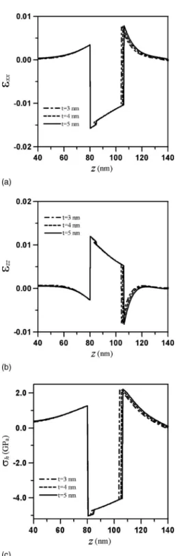
Figures2共a兲and2共b兲show normal strain componentsxx
and zz, respectively, of QD structure along the z-axis 共the
direction of QD growth兲 when the template layer is 5 nm thick. Kurdi et al. obtained similar tendency on strain distri-bution using the valence force field theory.8 These strain
components are not continuous across the
Si0.52Ge0.48/Si0.5Ge0.5 and Si0.5Ge0.5/Si interfaces, as one might expect from the theory of continuum mechanics. No-tice from Fig. 2, inside the template layer and the dot, the strain fieldsxxare compressive, whilezzare tensile.
More-over, inside the dot xxis less compressive than that in the
template layer. These results reveal that the lattice constants of the Si0.5Ge0.5template layer and the Si0.52Ge0.48quantum dot are larger than that of the Si substrate. The calculated strains have similar distributions but slightly differ in values for cases of different template layer thicknesses. In particu-lar, the difference in xxwithin the Si matrix共substrate and
cap layer兲 increases as the thickness t increases, while the difference inzz decreases.
The hydrostatic strain and uniaxial strain are defined re-spectively as
h=xx+yy+zz and u=zz−
共xx+yy兲
2 . 共5兲
The calculated results show that the hydrostatic strain is negative in the template layer and the QD, while the uniaxial strain is positive. The strain in the Si layer is small since Si is much stiffer than SiGe. Figure2共c兲shows the hydrostatic stress, h=xx+yy+zz, along the z-axis 共the direction of
QD growth兲. The strain fields obtained here will serve as inputs for the confinement potentials and electric structure calculations in the following section. Makeev and co-workers report similar phenomena for a pyramidal Ge QD using atomistic simulation.9,10
It is also of interest to point out that several studies have used Raman scattering to characterize the strain and
compo-sition of Si1−cGecfilms.12,19,20 The GeGe mode phonon
fre-quency induced by QD strain components can be written as19
=0+ 1
20共p zz+ 2 qxx兲, 共6兲
where0= 0.5468⫻1014s−1 is the frequency of Si0.52Ge0.48 bulk alloys,20and the Ge deformation potentials p and q are −4.7⫻1027 and −6.167⫻1027s−2, respectively.19 The aver-ages of calculated strain fields,xxand zz, inside the
quan-tum dot are −1.22⫻10−2 and 7.52⫻10−3, respectively, for a template layer thickness of t = 5 nm. Substituting these val-ues directly into Eq. 共6兲 leads to a phonon frequency of 296 cm−1. For the sake of comparison the same procedure is used to calculate a hut-shaped QD with the same thickness of template layer, and the strain-induced phonon frequency is 297 cm−1 instead. It is well-known that the phonon fre-quency depends not only on built-in strain but also on the exact composition of the dots. Nevertheless, these calculated phonon frequencies here are very similar to an experimental GeGe mode phonon frequency.12
IV. TRANSITION ENERGY
The confinement potential V for strained quantum-dot heterostructures can be written as the sum of energy offsets of the unstrained conduction共or valence兲 band Vbandand the strain-induced potential Vstrain,
V共r兲 = Vband共r兲 + Vstrain共r兲. 共7兲
The difference in the bandgap energies of the constituent materials of the heterostructure determines the contribution of Vstrain. Since strain effects induce an extra potential field
Vstrain, as suggested by the deformation potential theory,21 any alteration in the band structure and optical properties of a quantum-dot system calls for further investigation. The electric material properties used in this study are taken from Ref. 18and22–26.
The confinement potentials in strained semiconductor QDs, including the strain-induced effects, are piecewise con-tinuous functions of position. Figure 3 shows these poten-tials, along the z-axis共the direction of QD growth兲, for both electrons and holes. Notice that the⌬4valley in the Si matrix and the⌬2valley in the SiGe region are neglected. The con-duction band offset at each interface has been calculated, and their values for the minima conduction band as deduced from ⌬Ec⌬2
−⌬共Si
0.5Ge0.5/Si兲 and ⌬Ec⌬4 −⌬共Si
0.5Ge0.5/Si兲 are around −36 and 28 meV, respectively, for different thicknesses t. On the other hand, ⌬Ec⌬2
−⌬共Si
0.52Ge0.48/Si兲=−91, −93, and −95 meV, and⌬Ec⌬4
−⌬共Si
0.52Ge0.48/Si兲=33, 34, and 35 meV, for template layer thicknesses t = 3, 4, and 5 nm, respectively. Thus, the band offset remains at a nearly constant value at FIG. 2.共Color online兲Strain components, 共a兲 xxand共b兲 zz, and hydrostatic
stress,共c兲h=xx+yy+zz, plotted along the z-axis for various different template layer thicknesses.
FIG. 3. Energy diagrams of the strained SiGe/Si QD heterostructures plot-ted along the z-axis for template layer thicknesses t = 5 nm.
the Si0.5Ge0.5/Si interface. However, the band offset in-creases as the thickness t inin-creases at the Si0.52Ge0.48/Si in-terface.
The three-dimensional steady-state effective-mass Schrödinger equation helps to determine the behavior of in-dividual carriers in quantum-dot nanostructures. This paper numerically analyzes the Schrödinger equation using the same finite element package used above. The ground state energy levels of the conduction as well as the heavy-hole and light-hole bands are calculated. Figure4shows these ground state energy levels for cases of different template layer thick-nesses. Transition energy is defined as the difference between energy levels of the electron and the hole. These transition energies are related to the peaks of photoluminescence共PL兲 spectra. The optical conductivity peaks at particular wave-lengths of light that are more strongly absorbed. The calcu-lated fundamental transition energies are 0.804 and 0.810 eV for lens-shaped and hut-shaped QDs, respectively, with
thickness t = 5 nm, which agree well with the peak of experi-mental PL emission spectrum.12 The transition energies of lens-shaped QDs for t = 3 and 4 nm are 0.813 and 0.809 eV, respectively. These results suggest that the transition energy decreases as the template layer thickness increases.
Figure5 shows the probability density function profiles 兩兩2for the ground state in a quantum-dot nanostructure. Fig-ures 5共a兲 and5共b兲 are the probability density function pro-files of the electron state and the heavy-hole state, respec-tively, for the template layer thicknesses t = 5 nm. In Fig. 5共a兲, the electrons are attracted to the top of the SiGe QD and are confined in the Si capping layer. This result might be due to the fact that a SiGe quantum-dot heterostructure is a typi-cal type II transition material. In Fig. 5共b兲, the effect of the quantum-dot confines the hole in the template layer region right below the QD with a disklike shape. Other template layer thicknesses yield similar phenomena.
V. CONCLUSIONS
Based on the theory of linear elasticity, this paper ana-lyzed the strain fields induced by lattice constant mismatches in SiGe/Si quantum-dot heterostructures using finite element methods. This study used the calculated strains to evaluate the strain-induced phonon frequencies and found that they were consistent with experimental phonon frequencies. Fur-thermore, the energy levels and wavefunction distribution have been obtained by analyzing the three-dimensional steady-state effective-mass Schrödinger equation. The calcu-lated transition energies agreed well with previous experi-mental photoluminescence studies. Numerical results showed that transition energy decreases as the template layer thickness increases.
FIG. 4. Ground state energy levels of each band for different template layer thicknesses. The different lines correspond to the different energy bands.
FIG. 5.共Color online兲 Probability density function profiles for energy levels of the ground state corresponding to 共a兲 conduction band and 共b兲 heavy-hole band for template layer thickness t = 5 nm.
ACKNOWLEDGMENTS
This work is carried out in the course of research spon-sored by the National Science Council of Taiwan under Grant Nos. NSC94-2212-E-002-004 and NSC95-2221-E-002-041-MY3.
1D. Bimberg, M. Grundmann, and N. N. Ledentsov, Quantum Dot Hetero-structures共Wiley, West Sussex, 1999兲.
2P. Harrison, Quantum Wells, Wires and Dots: Theoretical and Computa-tional Physics共Wiley, West Sussex, 2000兲.
3H. Pettersson, R. J. Warburton, J. P. Kotthaus, N. Carlsson, M. E. Seifcrt,
and L. Samuelson,Phys. Rev. B60, R11289共1999兲.
4M. K. Kuo, T. R. Lin, K. B. Hong, B. T. Liao, H. T. Lee, and C. H. Yu, Semicond. Sci. Technol.21, 626共2006兲.
5V. Le. Thanh, P. Boucaud, D. Debarre, Y. Zheng, D. Bouchier, and J. M.
Lourtioz,Phys. Rev. B58, 13115共1998兲.
6P. H. Tan, K. Brunner, D. Bougeard, and G. Abstreiter,Phys. Rev. B68,
125302共2003兲.
7B. V. Kamenev, L. Tsybeskov, J. M. Baribeau, and D. J. Lockwood,Appl. Phys. Lett.84, 1293共2004兲.
8M. El. Kurdi, S. Sauvage, G. Fishman, and P. Boucaud,Phys. Rev. B73,
195327共2006兲.
9M. A. Makeev and A. Madhukar,Phys. Rev. Lett.86, 5542共2001兲. 10M. A. Makeev, W. Yu, and A. Madhukar,Phys. Rev. B68, 195301共2003兲.
11F. Schäeffler,Semicond. Sci. Technol.12, 1515共1997兲.
12I. Berbezier, M. Descoins, B. Ismail, H. Maaref, and A. Ronda,J. Appl. Phys.98, 063517共2005兲.
13L. B. Freund,Int. J. Solids Struct.37, 185共2000兲.
14V. T. Bublik, S. S. Gorelik, A. A. Zaitsev, and A. Y. Polyakov,Phys. Status Solidi B65, K79共1974兲.
15M. K. Kuo, T. R. Lin, B. T. Liao, and C. H. Yu, Physica E 26, 199共2005兲. 16T. R. Lin, M. K. Kuo, B. T. Liao, and K. P. Hung, Bull. Coll. Eng., Natl.
Taiwan Univ. 91, 3共2004兲.
17John H. Davies, D. M. Bruls, J. W. A. M. Vugs, and P. M. Koenraad,J. Appl. Phys.91, 4171共2002兲.
18M. E. Levinshtein, S. L. Rumyantsev, and M. S. Shur, Properties of Ad-vanced Semiconductor Materials共Wiley, New York, 2001兲.
19J. Groenen, R. Carles, S. Christiansen, M. Albrecht, W. Dorsch, H. P.
Strunk, H. Wawra, and G. Wagner,Appl. Phys. Lett.71, 3856共1997兲.
20H. K. Shin, D. J. Lockwood, and J. M. Baribeau,Solid State Commun.
114, 505共2000兲.
21S. L. Chuang, Physics of Optoelectronic Devices 共Wiley, New York,
1995兲.
22G. C. Van de Walle and R. M. Martin,Phys. Rev. B34, 5621共1986兲. 23G. C. Van de Walle,Phys. Rev. B39, 1871共1989兲.
24D. J. Paul,Semicond. Sci. Technol.19, R75共2004兲. 25M. M. Rieger and P. Vogl,Phys. Rev. B48, 14276共1993兲.
26L. Yang, J. R. Watling, R. C. W. Wilkins, M. Borici, J. R. Barker, A.