國 立 交 通 大 學
電子工程學系電子研究所
碩 士 論 文
40 奈米 1.0Mb 6T 管線化靜態隨機存取記憶體與
三步階升壓型字元線和位元線降壓和適應性電
壓偵測
40nm 1.0Mb 6T Pipeline SRAM with Three
Step-Up Word-Line, Bit-Line Under-Drive and
Adaptive Voltage Detector
研 究 生:廖 偉 男
指導教授:莊 景 德
40 奈米 1.0Mb 6T 管線化靜態隨機存取記憶體與三步
階升壓型字元線和位元線降壓和適應性電壓偵測
40nm 1.0Mb 6T Pipeline SRAM with Three Step-Up Word-Line,
Bit-Line Under-Drive and Adaptive Voltage Detector
研 究 生:廖偉男 Student:Wei-Nan Liao
指導教授:莊景德 Advisor:Prof. Ching-Te Chuang
國 立 交 通 大 學
電子工程學系 電子研究所碩士班
碩 士 論 文
A Thesis
Submitted to Department of Electronics Engineering and Institute of Electronics
College of Electrical and Computer Engineering National Chiao Tung University
In Partial Fulfillment of the Requirements for the Degree of
Master of Science in
Electronics Engineering
September 2012
Hsinchu, Taiwan, Republic of China
I
40 奈米 1.0Mb 6T 管線化靜態隨機存取記憶體與三步
階升壓型字元線和位元線降壓和適應性電壓偵測
學生:廖偉男 指導教授:莊景德教授
國立交通大學電子工程學系電子研究所
摘要
近幾年來,記憶體在許多電子產品中被廣泛運用,因為記憶體的高操作速度與高效 能。另外,因為靜態隨機存取記憶體也比其他種類的記憶體具有更高的操作速度,所以 靜態隨機存取記憶體在高性能微處理器的快取記憶體和嵌入式系統中更是被廣泛應用。 過去 20 年間,6T 靜態隨機存取記憶體因為有較高的操作速度與較緊密的面積,因此在 設計上仍然以 6T 靜態隨機存取記憶體為設計主流。但是隨著製程演進至深次微米等級 之後,製程變異會是影響 6T 靜態隨機存取記憶體存活的關鍵因素。在先進製程下,這 些製程變異會讓 6T 靜態隨機存取記憶體的讀或寫的能力受到嚴重的退化。除了讀寫能 力受到影響之外,特別是在低壓操作時,6T 靜態隨機存取記憶體幾乎是無法正常的運 作。 為了設計出能在先進製程下正常運作的 6T 靜態隨機存取記憶體,我們提出三步階 升壓型字元線技術、適應性數據感知寫入輔助技術、位元線降壓技術以及適應性電壓偵 測技術來提高讀寫能力與降低閘極氧化層被擊穿的機會。此外,為了提高操作速度我們 也運用管線化技巧。在本論文中,我們將這些技術、2 階級管線化技術與單電源電壓設 計在一顆 1.0Mb 高性能 6T 靜態隨機存取記憶體,並且透過下線將該晶片實現在 40 奈米 低功耗互補金屬氧化物半導體技術上。該晶片可以工作在寬電壓範圍從 1.2V 至 0.7V, 具有工作平率 [email protected] 和 25oC。I
40nm 1.0Mb 6T Pipeline SRAM with Three Step-Up Word-Line
and Bit-Line Under-Drive and Adaptive Voltage Detector
Student:Wei-Nan Liao Advisor:Ching-Te Chuang
Department of Electronics Engineering & Institute of Electronics
National Chiao-Tung University
ABSTRACT
In recent years, memories have been widely used for the most electronic products due to their high operation speed and high performance.Besides, Due to SRAMs have higher operating speed than other memory family, SRAMs have been widely used for the high-performance microprocessor cache and embedded system.During the past 20 years, standard 6T SRAM cell becomes the mainstream of SRAMs design due to its highest speed and compact area. However, with the scaling into the deep sub-micron of process, the process variation affects the subsistence of the 6T SRAM cell. In advance technology node, the read and write ability suffer a serious degradation by theses process variation. Especially, at low operation voltage, 6T SRAM cell almost couldn’t have normal operation.
In order to design the 6T SRAM that it can normal work in the advanced process, we proposed the Three Step-Up Word-Line technique, Adaptive-Data-Aware Write-Assist technique, Bit-Line Under-Drive Read-Assist technique, and Adaptive Voltage Detector technique to enhance the read/write ability and performance, and reduce the gate oxide to be punctured. Besides, in order to enhance operating speed, we also applied the pipeline technique to enhance the operating speed. In the thesis, we design a 1.0Mb high-performance 6T SRAM with these techniques with two stage pipeline technique with a single supply voltage, and implement by way of tape out in the 40nm Low- Power complementary metal-oxide semiconductor technology. The chip has wide voltage range from 1.5V to 0.6V, with operating frequency of [email protected] and 25℃.
I
誌
謝
本論文能順利完成,首先誠摯的感謝指導教授莊景德教授。在這兩年多的 研究生涯裡,莊老師除了在專業領域上以他豐富的知識給予耐心的指導之外,更 重要的是,讓我們很快就搭上最先端的研究,而省去獨自慢慢摸索的無奈歷程。 莊老師為人和藹可親以及對於研究上的嚴謹態度,讓我學得更多專業知識以外的 事物。 感謝博士班的連南鈞(Patrick)學長,在研究過程中給了許多的幫助。Patrick 學長研究與實務經驗充足,也在許多方面給了我指導與建議,讓我能夠快速的在 研究上步入軌道。另外感謝張琦昕學長,在畢業後仍不離不棄的給予我鼓勵並且 在我壓力大的時候帶我去發洩壓力,讓我可以順利的完成論文。至於實驗室的包 家豪、蔡明甫、朱俐瑋同學以及學長吳尚霖、學弟張智皓、黃騰頡、鍾兆貴還有 學妹林毓柔、楊邵喻、王唐瑄,也感謝你們能夠和我一起討論、運動、烤肉,也 因為有你們實驗室才能如此歡樂並且快樂的做研究。 感謝FARADAY 的學長們,使我可以提前了解業界的考量,並且以業界的標 準來設計晶片。也特別感謝各位學長們不吝嗇給予建議與協助,使晶片可以如期 下線。 最後,謹以此文獻給我摯愛的雙親,感謝你們能夠將我扶養成人,在我跌 跌撞撞的生涯裡給予最適時的幫助與鼓勵。 廖偉男 于新竹交大 2012.9.20I
Content
CHAPTER 1 INTRODUCTION ... 1
1.1 BACKGROUND ... 1
1.2 MOTIVATION AND GOALS ... 2
1.3 THESIS ORGANIZATION ... 2
CHAPTER 2 OVERVIEW OF THE DESIGN OF 6T SRAM ... 4
2.1 MEMORY FAMILY... 4
2.2 6TSRAM ... 5
2.2.1 Structure of 6T SRAM ... 5
2.2.2 Read Operation and Read Disturb of 6T SRAM... 6
2.2.3 Hold Static Noise Margin and Read Static Noise Margin ... 8
2.2.4 Write Operation and Half-Selected Read Disturb of 6T SRAM ... 10
2.2.5 Write Static Noise Margin and Write Margin and AC Write Margin ... 12
2.2.6 The Size and Layout of 6T SRAM ... 14
2.3 SRAMARRAY ARCHITECTURE ... 15
2.3.1 Memory Array ... 15
2.3.2 Differential Sensing and Large Signal Sensing Scheme ... 17
2.3.3 Non-Pipeline SRAM Design ... 21
2.3.4 Pipeline SRAM Design ... 22
2.4 GLOBAL VARIATION AND LOCAL VARIATION ISSUE ... 26
2.5 THE DESIGN METHODOLOGY OF 6TSRAM ... 28
2.5.1 Dual Supplies ... 29
2.5.2 Dynamic Bit-Line Level ... 31
2.5.3 Dynamic Word-Line Level ... 32
2.5.4 Negative Bit-Line Level ... 34
CHAPTER 3 DESIGN OF 1.0MB 6T PIPELINE SRAM WITH THREE STEP-UP WORD-LINE AND BIT-LINE UNDER DRIVE AND ADAPTIVE VOLTAGE DETECTOR SKILL 37 3.1 INTRODUCTION ... 37
3.2 PROPOSED BIT-LINE UNDER-DRIVE (BLUD)TECHNIQUE ... 40
3.3 PROPOSED THREE STEP-UP WORD-LINE (TSUWL)TECHNIQUE ... 47
3.4 PROPOSED ADAPTIVE VOLTAGE DETECTOR (AVD)TECHNIQUE ... 57
3.5 MACRO IMPLEMENTATION AND SIMULATION RESULT ... 58
II
3.7 IMPLEMENTATION AND MEASUREMENT RESULT OF TEST CHIP ... 70
CHAPTER 4 CONCLUSIONS ... 75
REFERENCE OF CHAPTER 2 ... 76
I
List of Figures
Fig. 2-1 Traditional 6T SRAM cell ... 5
Fig. 2-2 Voltage Transfer Curve (VTC) of CMOS inverter [2-1] ... 6
Fig. 2-3 Read operation ... 7
Fig. 2-4 Stability ratio [2-2] ... 8
Fig. 2-5 Butterfly curve of HSNM ... 9
Fig. 2-6 The HSNM and RSNM butterfly curve ... 10
Fig. 2-7 Write operation ... 11
Fig. 2-8 Half-Selected Read Disturb Voltage of 6T SRAM cell [2-2] ... 12
Fig. 2-9 Half-Selected Disturb of the 6T SRAM array (For Write operation) [2-2] ... 12
Fig. 2-10 Butterfly curve of WSNM ... 13
Fig. 2-11 The definition of the Write Margin (WM) [2-3] ... 14
Fig. 2-12 Transistor size ratio in 6T SRAM[2-2] ... 15
Fig. 2-13 The layout of the 6T SRAM in advanced process technology ... 15
Fig. 2-14 Array architecture of an 2Nx2M memory array [2-1] ... 16
Fig. 2-15 SRAM critical path [2-5] ... 17
Fig. 2-16 Differential sense amplifier [2-1] ... 18
Fig. 2-17 Large signal sensing scheme of IBM Cell processor [2-12, 2-13] ... 20
Fig. 2-18 Large signal sensing scheme [2-11] ... 20
Fig. 2-19 Non-Pipeline SRAM operation diagram ... 22
Fig. 2-20 The design of 11FO4 cycle time between cycle boundary [2-6] ... 23
Fig. 2-21 Local store macros in Streaming Processor Element (SPE) [2-6] ... 24
Fig. 2-22 Pipeline SRAM operation diagram ... 25
Fig. 2-23 Global variation and Local variation of threshold voltage [2-2] ... 26
Fig. 2-24 The effect of local variation, (a) Write mode worse case, and (b) Read mode worse case 28 Fig. 2-25 Dual voltage domain of IBM Cell processor [2-12, 2-13] ... 30
Fig. 2-26 Dual voltage domain of 6T SRAM floor-plan [2-10]... 30
Fig. 2-27 VMIN and stability range of dual supply [2-22] ... 31
Fig. 2-28 Bit-Line charge-recycling technique [2-23] ... 32
Fig. 2-29 RSNM improvement with lower VWL, (b)WSNM decade with lower VWL[2-24] ... 33
Fig. 2-30 RSNM is improved by suppressing WL level [2-16] ... 33
Fig. 2-31 Boosting WL technique of the 6T SRAM [2-15] ... 34
Fig. 2-32 Multi-Step WL technique [2-17, 2-18]... 34
Fig. 2-33 Negative ground voltage of the 6T SRAM [2-14]... 35
II
Fig. 3-1 Standard 6T SRAM cell schematic in Read mode ... 40
Fig. 3-2 Standard 6T SRAM cell butterfly curves under best and worst case ... 41
Fig. 3-3 Bit-Line level in dual supply SRAM [3-22]... 42
Fig. 3-4 VBLH Bit-Line regulation system and yield improvement [3-21] ... 42
Fig. 3-5 Bit-Line Under-Drive (BLUD) circuit ... 43
Fig. 3-6 Large signal sensing circuit with Cross couple pair circuit ... 44
Fig. 3-7 Timing diagram for BLUD during read cycle ... 45
Fig. 3-8 The BLUD technique improves Read Margin with 3-σ variation ... 46
Fig. 3-9 The BLUD technique improves LBL falling time with 3-σ variation (read 0) ... 47
Fig. 3-10 RSNM increase with suppress word-line supply ... 48
Fig. 3-11 WSNM decrease with suppress word-line supply ... 48
Fig. 3-12 (a) Word-Line Under-Drive (WLUD) circuit (b) Previous Read Assist circuit (PRA) (c) Multi-Step Word-Line Control (MWC) circuit (d) Step-Up Word-Line (SUWL) circuit ... 50
Fig. 3-13 Three Step-Up Word-Line (TSUWL) circuit ... 51
Fig. 3-14 Timing diagram for TSUWL during read cycle ... 52
Fig. 3-15 Spice simulation results for TSUWL with different delay time ... 53
Fig. 3-16 Spice simulation results for read speed comparison of propose and precious ... 54
Fig. 3-17 Spice simulation results for WL rising time comparison of propose and precious... 55
Fig. 3-18 Spice simulation results for butterfly curve improvement with 3-σ of variation comparison of TSUWL and BLUD... 55
Fig. 3-19 Spice simulation results for Read Margin (RM) improvement with 3-σ variation comparison of TSUWL and BLUD... 56
Fig. 3-20 Spice simulation results for Read Margin (RM) improvement with 3-σ variation comparison of TSUWL and BLUD ... 56
Fig. 3-21 Adaptive Voltage Detector (AVD) circuit ... 57
Fig. 3-22 Timing diagram for AVD during read/write cycle... 58
Fig. 3-23 Adaptive-Data-Aware Write-Assist (ADAWA) circuit of 6T SRAM ... 59
Fig. 3-24 Proposed ADAWA_WEB tracking control circuit ... 60
Fig. 3-25 Timing diagram for ADAWA during write cycle ... 60
Fig. 3-26 The ADAWA technique improves AC Write Margin (ACWM), Vmin with 3-σ variation .... 61
Fig. 3-27 The ADAWA technique improves WSNM with 3-σ variation ... 61
Fig. 3-28 The ADAWA technique improves Write time with 3-σ variation ... 62
Fig. 3-29 Spice simulation results for Write Margin (WM) improvement with 3-σ variation comparison of TSUWL and ADAA ... 62
Fig. 3-30 Critical path of 1.0Mb two stages pipeline 6T SRAM macro ... 63
Fig. 3-31 Local Evaluation Circuit (LEV) ... 65
Fig. 3-32 Read path (Word-Line to Output latch)... 66
III
Fig. 3-34 Simulation waveform in Write/Read “0” operation ... 68
Fig. 3-35 Simulation waveform in Write/Read “1” operation ... 68
Fig. 3-36 Test flow of the implemented chip ... 69
Fig. 3-37 Die photo ... 70
Fig. 3-38 Measured error free full functionality die yield (without redundancy) versus VDD (=VCC) for FF (58 dies), TT (65 dies), and SS (53 dies) corners (without read/write assist technique) ... 70
Fig. 3-39 Measured error free full functionality die yield (without redundancy) versus VDD (=VCC) for FF (58 dies), TT (65 dies), and SS (53 dies) corners (with TSUWL and ADAWA technique) ... 71
Fig. 3-40 Measured error free full functionality die yield (without redundancy) versus VDD (=VCC) for FF (58 dies), TT (65 dies), and SS (53 dies) corners (with TSUWL and BLUD technique) ... 71
Fig. 3-41 Measured Bit Failure Rate (BFR) at TT corner (Write-Assist: TSUWL and ADAWA; Read-Assist: TSUWL and BLUD) ... 72
Fig. 3-42 Measured Bit Failure Rate (BFR) at FF corner (Write-Assist: TSUWL and ADAWA; Read-Assist: TSUWL and BLUD) ... 72
Fig. 3-43 Measured Bit Failure Rate (BFR) at SS corner (Write-Assist: TSUWL and ADAWA; Read-Assist: TSUWL and BLUD) ... 73
Fig. 3-44 Measured Failure Bit Count Improvement with TSUWL and Boosting WL technique ... 74
1
Chapter 1
Introduction
1.1 Background
During the past 20 years, Moore’s Law told us that the density of the chip capacity is doubled per 18 month. Today, the CMOS technology still follows this rule. In addition to performance, the chip cost and complexity are enhanced with the advanced technology. However, with the scaling into the deep sub-micron of process, the size of device and Vth are reduced. But the process variation will become serious
issue, because the sigma of local Vth variation is larger than that of the global Vth
variation in advance technology.Therefore, we must consider the global variation and the local variation in previous simulation. However, the performance of manufactured transistor may be different to previous simulated value and lead to system functional error. This could result the degradation to the yield during chip manufacture.
In accordance with ITRS’s predictions, memory area will occupy nine-tenths area of the chip. Static Random Access Memory (SRAM) is an important role, because it would dominate the area, performance and power of the SOC chip.Besides, we know that high performance multi-core processors and clouding computing usually need high speed and large capacity SRAM to do data processing. In order to implement these electronic application products, the most important issue is how to design a high performance SRAM.
2
1.2 Motivation and Goals
Nowadays, In order to implement high performance electronic application products, the Static Random Access Memory (SRAM) is an important role. However, with the reducing supply voltage and scaling process, the transistor characteristic variability would affect the subsistence of the standard SRAM in advance technology node. The degradation of the read and write static noise margin (SNM) is the most crucial issue. From past decades, much circuit technique solutions have been proposed in order to reduce the variation and shifting issue. However, static noise margin of SRAM is contradictory condition between read and write mode. Therefore, we try to propose different circuit technique to separately solve the read and write issue.In thesis, we must focus on the read and write assist circuit technique in order to enhance read and write ability of SRAM. In addition to these read/write assist circuit technique, we want to have widely operation voltage range. Even at low supply voltage, we wish 6T SRAM could also have good manufacturability and yield with these read and write assist circuit technique.
1.3 Thesis Organization
In the following of the thesis, Chapter 2 discuss the basic operation concept of traditional 6T SRAM and its design issue. Besides, we would compare the difference between non-pipeline SRAM design and pipeline SRAM design in Chapter 2. In addition to these concepts, the reliability issue and some design methodology would be also mentioned in this Chapter. Chapter 3 demonstrates “40nm 1.0Mb high performance 6T Pipeline SRAM with Three Step-Up Word-Line (TSUWL) and Bit-Line Under-Drive (BLUD) and Adaptive Voltage Detector (AVD)” design.In this Chapter, Variation Tolerant TSUWL is proposed to improve the read and write
3
stability of 6T SRAM. Variation Tolerant Bit-Line Under-Drive scheme for SRAM stability enhancement for low voltage operation. Variation Tolerant boost control scheme using Adaptive Voltage Detector circuit to mitigate gate dielectric over stress. The design issue and test flow and chip measurement result would be also discussed in Chapter 3. In the end, Chapter 4 makes a conclusion to this thesis.
4
Chapter 2
Overview of the design of 6T
SRAM
2.1 Memory Family
Memory always occupies over 90% area of the current System on Chip (SOC). As a result, memory always dominates the overall performance of one system. In order to store data, we always used the Random Access Memory (RAM) in the integrated system (IC). Besides, memory family could basically be divided into two categories: volatile memory and nonvolatile memory. RAMs is always associated with volatile memory which the storage data would loss if the power turn off. In contrast, nonvolatile memory would keep the storage data if the power off.
RAMs have been widely used for the most embedded system due to their higher access speed than other memory family. Besides, volatile memory could basically be divided into two categories: Dynamic RAM (DRAM) and Static RAM (SRAM). DRAM has more compact density than SRAM, because DRAM can be built by one transistor and one capacitance. For the past decade, conventional 6T SRAM is always the mainstream to the cache memories in high performance system due to it has the highest operation speed which could reach several hundred Mega Hertz or even Giga Hertz than DRAM. Nowadays, DRAM is currently the major storage device of most SOC due to it has more compact density.
5
design of 6T SRAM will be faced with several challenges. We must consider these issues which are the process variation and the leakage due to the Read/Write ability suffers a serious degradation in these issues. In order to reduce the process variation and the leakage, we must focus on how to design an efficient circuit technique and understand the basic operation of 6T SRAM.
2.2 6T SRAM
2.2.1 Structure of 6T SRAM
BL
BLB
WL
VDD
VDD
Q
QB
M1
M2
M3
M4
M5
M6
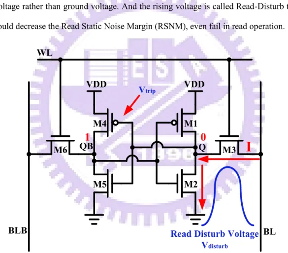
Fig. 2-1 Traditional 6T SRAM cell
In Fig. 2-1 shows the widely common used traditional 6T SRAM cell. For this cell, it includes three control signals and six transistors. Three control signals contain Word-Line (WL) and one pair of Bit-Lines (BL and BLB). Six transistors of the cell contain two pass-gate n-type transistors (M3 and M6), and two pull-up p-type transistors and two pull-down n-type transistors, so the cell is called 6”T” (Transistor)
6
cell. Two inverters (M1-M2 and M4-M5) are to combine to form one cross couple latch in this cell. This cell could use the cross couple latch to lock value at logic “1” or “0” due to the voltage transfer curve (CVT) of the cross couple latch has only two stable points. In fact, there is one meta-stable point when slope is positive one, but it’s not easy to exist (show in Fig.2-2). This Bit-Line pair is connected to the source node of pass-gate n-type transistors. Besides, two pass-gate n-type transistors could be seen as port to access the storage data in this cell. And “Q” and “QB” are storage nodes. Word-Line signal is used to enable this cell, and then the data could be passed in or passed out from this Bit-Lin pair.
Fig. 2-2 Voltage Transfer Curve (VTC) of CMOS inverter [2-1]
2.2.2 Read Operation and Read Disturb of 6T SRAM
Before the read operation, all of Bit-Line pairs of 6T SRAM cell are pre-charged to high voltage (VDD) at standby mode. At read mode, assume the cell storage data which “Q” storage node is “0” (GND) and “QB” storage node is “1” (VDD) (Fig. 2-3). When once the signal of Word-Line goes high, two pass-gate n-type
7
transistors (M3 and M6) are turned on for accessing storage data. The storage node “0” side will discharge the Bit-Line voltage to ground level (through M3 and M2). However, on the other side of the storage node “0”, the storage node “1” will uphold the high level due to the storage node “1” and BLB are the same high level. According to this operation flow, the storage data can be easily passed to Bit-Line. And then, in order to get exact storage data on output pin, we must use additional peripheral read circuit to get the storage data from Bit-Lin.
BL BLB WL VDD VDD Q QB
1
0
I
Read Disturb Voltage Vdisturb M1 M2 M3 M4 M5 M6
Fig. 2-3 Read operation
At read mode, this cell had a thorny problem that would to hurt the original storage data. Fig. 2-3 shows the pass-gate n-type transistor (M3) and the pull-down n-type transistor (M2) form a voltage divider. In this case, we assume node “Q” is “0” (GND). When the signal of Word-Line goes high level, node “Q” would be rose to a voltage rather than ground voltage. This situation was called Read-Disturb voltage. Besides, because of the Read-Disturb voltage, the read stability suffers a serious
8
degradation. When the Read-Disturb voltage goes over the trip voltage of the opposite inverter, the storage node “1” would be flipped to “0”.
Fig. 2-4 shows the stability ratios. At 90 nm technology node, the cell switch-point and read down-level began to overlap. That would affect the design of a high yield SRAM in advance technology node.
Fig. 2-4 Stability ratio [2-2]
2.2.3 Hold Static Noise Margin and Read Static Noise Margin
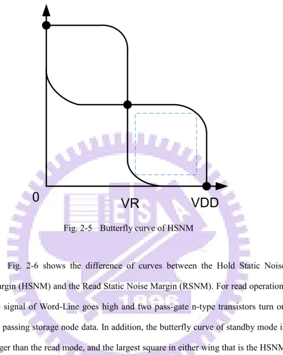
In order to evaluate the read ability of 6T SRAM, the Static Noise Margin (SNM) is an important indicator. First of all, we can use the Voltage Transfer Curve (VTC) to get the butterfly curve through switch the axis of any one of the Voltage Transfer Curve (VTC). And then, we can get the Static Noise Margin (SNM) by the butterfly curve. Fig. 2-5 shows the butterfly curve of the Hold Static Noise Margin (HSNM). We can get the HSNM curve at standby mode due to the standby mode operation of 6T SRAM is exactly a cross coupled pair latch. Besides, we can see it has two “wings” and the largest tolerable square of these two wings chooses the smaller one to use definition the Hold Static Noise Margin (HSNM).
9
VDD
VR
0
Fig. 2-5 Butterfly curve of HSNM
Fig. 2-6 shows the difference of curves between the Hold Static Noise Margin (HSNM) and the Read Static Noise Margin (RSNM). For read operation, the signal of Word-Line goes high and two pass-gate n-type transistors turn on for passing storage node data. In addition, the butterfly curve of standby mode is larger than the read mode, and the largest square in either wing that is the HSNM (standby mode) larger than the RSNM (read mode). Therefore, the minimum RSNM also could directly defined as the voltage difference between the trip voltage of inverter and the Read-Disturb voltage. If any other of RSNM wing becomes to “0” or under the zero, the destructive read operation will occur the read fail.
10
VDD
VR
0
VDD
VL
HSNM
RSNM
Fig. 2-6 The HSNM and RSNM butterfly curve
2.2.4 Write Operation and Half-Selected Read Disturb of 6T SRAM
Before the signal of Word-Line goes high, the write data must be ready on the Bit-Line pair. Fig. 2-7 shows a write mode, we assume the storage node “Q” is “0” and the storage node “QB” is “1” and we want to write “0” data to the storage node “QB”. In this case, the Bit-Line of the storage node “QB” side should be prepared to “0”. And then, when the signal of Word-Line goes high, the storage node “QB” data will discharge to ground level by pull-up p-type transistor (M4) and pass-gate n-type transistor (M6). This write operation is successfully, but it still has chance to happen write fail. If the storage node “QB” data is not lower to trigger the tip voltage of opposite inverter, then this write operation is fail.
11 BL BLB WL VDD VDD Q QB M1 M2 M3 M4 M5 M6
1
0
I
0
1
Fig. 2-7 Write operation
However, the most common seem problem to 6T SRAM Array is the Half-Selected Read Disturb issue (Fig. 2-8). Fig. 2-9 shows a write mode example. When the signal of WL1 goes high, the Column 1 (COL1) is selected for write operation and the Column 0 (COL0) is not selected for read operation. Under this situation, the Column 0 (COL0) cell can occur the Half-Selected Read Disturb. But the Half-Selected Read Disturb issue is unwanted. Because of the other standby cells would affect the storage data by this issue.
12
Fig. 2-8 Half-Selected Read Disturb Voltage of 6T SRAM cell [2-2]
Fig. 2-9 Half-Selected Disturb of the 6T SRAM array (For Write operation) [2-2]
2.2.5 Write Static Noise Margin and Write Margin and AC Write
Margin
Fig. 2-10 shows the butterfly curve of write operation. In a successfully write operation, the butterfly curve must be open with only one interest point. By definition, this butterfly curve like be combined by RSNM and HSNM. Besides, we also can find a largest tolerable square like RSNM or HSNM on this curve. But there is also write
13
fail problem for write operation. If the WSNM becomes to 0 or under the zero or more than one interest point, the write operation will fail.
To evaluate the write performance, the Write Margin (WM) [2-3, 2-4] is also an important indicator. Before the write operation, both of BL and BLB have to set at high level (logic one). During the write operation, we sweep down the Bit-Line voltage of the storage node “1” side of the cell from high level to ground level. Afterwards, when the storage node “1” flip, the Bit-Line voltage at this moment is defined as Write Margin (WM) (Fig. 2-11).
During write operation at the same Word-Line pulse width, we change the Bit-Line voltage of the storage node “1” side of the cell from high level to ground level. At some Bit-Line voltage the cell storage node “1” will be suddenly flip, and the Bit-Line voltage at this moment is defined as ACWM.
VDD
VR
0
VDD
VL
14
Fig. 2-11 The definition of the Write Margin (WM) [2-3]
2.2.6 The Size and Layout of 6T SRAM
In order to keep the read stability, the VREAD (Read-Disturb voltage) must be
small. So, the pass-gate n-type transistor should be weaker than pull-down n-type transistor (Fig. 2-12). To maintain the write ability, the pass-gate n-type transistor should be stronger than pull-up p-type transistor (Fig. 2-12). In addition, for keep the stability at the standby mode, the pull-down n-type transistor cannot be too stronger compares to pull-up p-type transistor (Fig. 2-12). As a result, the size of each transistor of the 6T SRAM cell is specific designed to ensure maximize the read and hold stability and the write ability.
Starting around 90nm node [2-2], the Thin-Cell layout of the 6T SRAM cell becomes the mainstream due to the Thin-Cell of layout style could reduce BL loading to improve performance and noise immunity. Fig. 2-13 shows the layout of 6T SRAM which uses a single direction poly-silicon to improve manufacturability and yield.
15
Fig. 2-12 Transistor size ratio in 6T SRAM[2-2]
Fig. 2-13 The layout of the 6T SRAM in advanced process technology
2.3 SRAM Array Architecture
2.3.1 Memory Array
For current System on Chip (SOC), memory always be build in the integrated system (IC) as the storage media. These cells are usually formed into an array to enhance the area efficiency and to easy access. In traditional SRAM architecture design, all of the SRAM cells are put together with the peripheral circuit such as Row/Column decoder and Sense Amplifier (SA) are placed next to the SRAM to control Read/Write operation (Fig. 2-14). In this architecture, in order to control pass-gate of all the row direction cells, the signal of Word-Line (WL) is usually a row
16
direction signal. And the Bit-Line (BL) is a signal of column direction that can pass in or out the data from the SRAM cell. So, if we want to select one cell for read or write operation, both the Word-Line (WL) and Bit-Line (BL) must be activated. When the interest cell is selected, the read or write operation is depend on the signal of write enable. However, if the number of the row or column cell increase, the total capacitance and resistance will increase on Word-Line (WL) and Bit-Line (BL), and thus increasing the transient response. In order to reduce the transient response issue, we can use the Hierarchical Word-Line technique and the Hierarchical Bit-Line technique. These two techniques not only reduce the Word-Line loading and the Bit-Line loading but also reduce the charge injection into SRAM cell and the transient response, and thus improving the performance, power and noise margin [2-2].
17
Fig. 2-15 SRAM critical path [2-5]
2.3.2 Differential Sensing and Large Signal Sensing Scheme
In order to get exact storage data on output pin, we must use additional peripheral read circuit to get the storage data from Bit-Lin. The sensing scheme could basically be divided into two categories: differential sensing scheme and large signal sensing scheme. The differential sensing is also celled the small signal sensing in conventional sensing scheme. In order to get the logic “0” or “1” signal from the amplified signal of differential sense amplifier, the basic idea of the differential sensing scheme is to sense the voltage difference between BL and BLB with amplify. To use a cross-couple latch (Q1, Q2, Q3 and Q4) and two access transistors (Q5 and Q6) are to combine to form a conventional differential sensing scheme (Fig. 2-16). It is similar to 6T SRAM but the sizing and the design are different. During read operation, after the Word-Line signal is enabled and the storage node data passed to the Bit-Line, one of the Bit-Line will begin to go low. If the voltage difference between BL and BLB has enough voltage to enable the differential sense amplifier,
18
the sense amplifier enable (SAE) signal would go high and activate the sense amplifier. Then, the Bit-Line pair will be fully separated and we can get a fully logic “0” or “1”. The differential sensing scheme usually co-operate with long Bit-Line structure which means there are many cells along the Bit-Line (usually more than hundred cells). In the long Bit-Line structure, due to the Bit-Line loading would become very heavy, the read time would suffer a serious degradation from the storage node data pass to Bit-Line. Therefore, in order to improve the read time, the long Bit-Line structure must be co-operated with the differential sensing scheme.
19
With the technology node goes the deep sub-micron of process, the leakage issue becomes a critical issue due to the charge into the cell will become very serious in the long Bit-Line structure. Even the Word-Line was turned off, the standby cell could be flip by the large leakage current that would result retention fail. And the differential sensing scheme also may fail to sense Bit-Line signal by the leakage current. Base on this issue, the Bit-Line length must be decreased and co-operate with short Bit-Line structure. In the short Bit-Line structure, the most common used length is about 8, 16, or 32 cells on Bit-Line. So, the total leakage current could be reduced and the read time could be also reduced. Therefore, the short Bit-Line structure must be co-operated with the large signal sensing scheme. The large signal sensing scheme has been used to sense the data on local Bit-Line [2-10, 2-11, 2-12 and 2-13]. At this scheme, the most common used one transistor or one inverter to detect the signal on the Bit-Lines. When the Bit-Line voltage goes lower than the sensing transistor or sensing inverter, the data of the Bit-Line will be passed out such as to Global Bit-Line and next stage circuit. Besides, the short Bit-Line structure can reduce the Bit-Line loading, and the storage node data pass to the Bit-Line will be faster. Due to the large signal sensing scheme is a single ended sensing, so the leakage is half to the differential sensing where both BL and BLB must be connected on the differential sensing amplifier. And the large signal scheme is easier to implement than the differential sensing scheme which is not easier to optimize the gain. For short Bit-Line structure with the large signal scheme, the area overhead was a disadvantage. Because of the short Bit-Line structure needs many sensing transistors or sensing inverters in each column, the area overhead is larger than the long Bit-Line structure. Fig. 2-17 and Fig. 2-18 show the typical the large signal sensing scheme.
20
Fig. 2-17 Large signal sensing scheme of IBM Cell processor [2-12, 2-13]
21
2.3.3 Non-Pipeline SRAM Design
Fig. 2-19 shows a Non-Pipeline SRAM operation diagram. When the Clock rising edge coming, the input address will be launched and decoded at the same time. Next the Finite State Machine (FSM) will control the WLE signal to enable Word-Line signal to perform read or write operation. Due to the WLE signal enable, the pre-charge circuit is turned off. In Non-Pipeline SRAM design, the WLE signal can be seen as internal Clock. For read operation, Local Bit-Line (LBL) and Global Bit-Line (GBL) will get the read data from the storage node data of the 6T SRAM cell. Then, we can utilize the replica control circuit to perform dummy read or write operation for making the WLE signal goes low to turn off Word-Line and enable Global Bit-Line (GBL)/Output latch. When the WLE signal goes low, the pre-charged circuit will be turned on again. This is a completely procedure of read operation in Non-Pipeline SRAM.
22
Fig. 2-19 Non-Pipeline SRAM operation diagram
2.3.4 Pipeline SRAM Design
Ultra high performance system utilizes the Pipeline SRAM to enhance the performance. Fig. 2-20 [2-6] shows the best of the operating time in a cycle is 11 Fan-Out-Of-4 (FO4). Fan-Out-Of-4 (FO4) means an inverter can drive four identical copies. The time of only 5 to 8 FO4 is used to operate for function and distribution due to the output delay of L2 and the setup time of the L1 should be removed. Hence, in Pipeline SRAM design, how to balance the operating time in every cycle is an important issue. WLE WLE BL Restore Pre-charge Disable WL
1 Cycle
Decoder Launch ADD. PRE-CHARGE LBL GBL Data-Out Latch LBL+ GBL GBL Latch Data-Out Latch23
Fig. 2-20 The design of 11FO4 cycle time between cycle boundary [2-6]
Fig. 2-21 [2-6] shows the macro of IBM fully Pipelined Embedded SRAM in the Streaming Processor of the cell processor. Starting operating SRAM is from the 3rd cycle to 5th cycle. At the 3rd cycle, one of Local Word-Line (LWL) signals will be decoded and latched in Word-Line driver. At the 4th cycle, the Local Word-Line (LWL) will be enabled to perform read or write operation. By the way, the write operation is finished in this cycle. In the read operation, the Bit-Line (BL) data utilizes the sense amplifier to sense and keep the data until the Read Latch (RL) captures it in the beginning of the 5th cycle. The 5th cycle is used to pass the read data from the Read Latch (RL) to next stage.
24
Fig. 2-21 Local store macros in Streaming Processor Element (SPE) [2-6]
Fig. 2-22 shows the timing diagram of the two stage pipeline design. In order to implement the two stage pipeline design, it has to need three components which are input latch, middle latch and output latch. Input latch is composed of the L1 latch and the L2 latch, it is used to capture input the address data and launch the pre-decode data to middle latch. Middle latch is L1 latch and always placed next to Word-Line (WL) driver, it is used to latch the pre-decode data and enable Word-Line (WL) driver. Output latch is composed of the L1 latch and the L2 latch, it is used to capture the signal of Global Bit-Line (GBL) and launch to output node. The L1 latch is utilized capture pre-data at negative edge of Clock and launch data to next stage at positive edge of Clock. Next, the L2 latch captures pre-data at positive edge of Clock and launch data to next stage at negative edge of Clock. The L1 latch and the L2 latch are to combine to form a Flip-Flop.
25
Fig. 2-22 Pipeline SRAM operation diagram
Because of this architecture is edge control, so there is no Finite State Machine (FSM) and replica circuit to control any internal signals in this architecture. Besides, all of the operating such as decoding and enable Word-Line (WL) to data output latch are only operated at the positive edge Clock, and the negative edge Clock is only used to pre-charge Bit-Line (BL) and Global Bit-Line (GBL). The fully operation in pipeline: at the 1st cycle for decoding address signal, at the 2nd cycle for enable Word-Line (WL)
L2
L1
L1
LCB
WL
CLK for L2 (Input Latch)I (Middle Latch)M
L2
L1
(Output Latch)OL1
L2
L1
L2
L1
L2
L1
L2
Decoder Enable WL Disable Pre-Charge LBL GBL GBL Latch DO L2 L1 (Output Latch)O L2 L1 (Input Latch) I L1 LCB WL CLK for L2 (Middle Latch)M Capture2nd ADD. 2Launchnd ADD. Decode OutputCapture Decode OutputLaunch @ Output LatchCapture Data Launch Output Latch Data
1 Cycle
1 Cycle
1 Cycle
1 Cycle
L1
L2
L1
L2
L1
L2
L1
L2
Decoder LBL GBL GBL Latch DO Enable WL Disable Pre-Charge L2 L1 (Output Latch) O L2 L1 (Input Latch) I L1 LCB WL CLK for L2 (Middle Latch)M Capture26
and sensing data to Global Bit-Line (GBL) latch, at the 3rd cycle for available output data. By the way, when the operating of middle latch is ongoing, the new address will be continuing to decode in the input latch.
2.4 Global Variation and Local Variation Issue
When the real chip was implemented, there must exist variation factor due to foundry makes the real physical device is different. At the CMOS technology process, because of these variations can appear on the threshold voltage (Vth), the current drive
ability and the leakage of the transistor may be decrease and larger. These problems would affect the functionality and the power consumption. The most common reasons are the lithography variation at each process, the concentration fluctuation of the doping and the line edge roughness, etc. The threshold voltage (Vth) variation could
basically be divided into two categories: Global variation and Local variation [2-7]. Global variation is also celled intra-die variation that means it between die to die. Local variation is also called intra-die variation that means the device variation at the same die. Fig. 2-23 shows the case for threshold voltage variation (δVt) , the variation
can be expressed as (1) [2-7]
δVt = ∆Vt−GLOBAL + δVt−LOCAL (1)
27
For Global variation, when every time we make the real chip at different corners, the gate length, gate width, gate oxide thickness and channel doping concentration would be different [2-8, 2-9]. The different process condition may affect different die. If we compare with PSNS and PFNF, the characteristic would vary inter dies. In addition, assume the two same devices at different location in the same die. We can find the threshold voltage (Vth) of device not the same with the same size of device. In
this case, it called Local variation. But the doping concentration is random and follows the statistical Gaussian-Distribution. For this reason, Local variation is unpredictable and hard to be controlled.
However, with the process technology node goes the deep sub-micron, the gate length is very short and the doping concentration is much less. At the advance technology design phase, the variation would become a critical problem. Both Global variation and Local variation issues also affect the characteristic of 6T SRAM. For the read operation, if Global variation at PSNF and Local variation of the each transistor of 6T SRAM cell shows in Fig. 2-24(b), the Read Static Noise Margin (RSNM) would be reduce even equal to zero or less than zero. Because of the high Vt M4 and
the low Vt M5 are to combine to form a higher Read-Disturb voltage with the high Vt
M1 and the low Vt M2 are to combine to form a smaller trip voltage of inverter such
as a worst case for read mode. Next, for the write operation, if Global variation at PFNS and Local variation of the each transistor of 6T SRAM cell shows in Fig. 2-24(a), the Write Static Noise Margin (WSNM) would be reduce even equal to zero or less than zero. Because of the high Vt M5 and the low Vt M3 are to combine to
form a higher write trip voltage with the high Vt M1 and the low Vt M2 are to
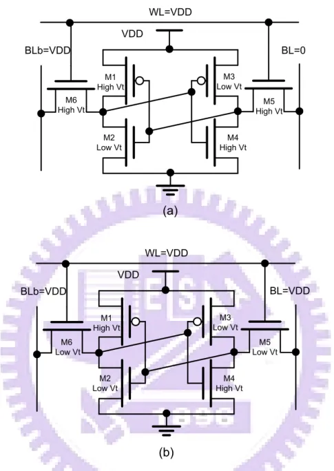
28 M1 High Vt M2 Low Vt M3 Low Vt M4 High Vt M5 High Vt VDD M6 High Vt BLb=VDD WL=VDD BL=0 (a) M1 High Vt M2 Low Vt M3 Low Vt M4 High Vt M5 Low Vt VDD M6 Low Vt BLb=VDD WL=VDD BL=VDD (b)
Fig. 2-24 The effect of local variation, (a) Write mode worse case, and (b) Read mode worse case
2.5 The Design Methodology of 6T SRAM
There several critical issue of 6T SRAM such as Read-Disturb voltage, Half-selected Disturb problem, Static Noise Margin (SNM), leakage and variation, etc have been discussed in the Chapter 2. Unfortunately, with the technology node goes the deep sub-micron of process, these issues will become more serious than before the discussing. In recent years, in order to enhance survival of 6T SRAM at advance
29
technology node, there has been a dramatic increase research concerned with how to improve the read/write ability and Static Noise Margin (SNM). In fact, the most common methodology to improve the read/write ability is four: 1) Dual Supplies 2) Dynamic Bit-Line level 3) Dynamic Word-Line level 4) Negative Bit-Line level. We would discuss these methods below.
2.5.1
Dual Supplies
In order to improve the performance of 6T SRAM such as the read and write ability, the memory array and local control circuits use the difference supply voltage. For increasing the read ability or the Static Noise Margin, we could increase the cell supply voltage or a negative supply voltage of cell. For increasing the write ability, we could reduce the supply of the cell. However, in order to achieve these targets, the easiest way is to use the second power source, so that the supply voltage of cell and logic circuit are separated. In order to have the best performance of the circuit, the most common used higher supply voltage is the critical path of the circuit. It usually sets a supply voltage 150mV – 200mV higher than the logic supply voltage to ensure cell stability and improve performance. And the critical path of circuit can also be on higher supply such as the Word-Line driver, decoder and write driver. However, the implementation of dual supplies is too expensive, so we need to so consider impact to overall system cost overhead when designing with dual supply grids. Fig. 2-25 and Fig. 2-26 show the dual supplies. These two examples used higher supply voltage in memory cell, the Word-Line driver, second level decode and write driver. Fig. 2-27 shows VMIN and stability range of dual supply.
30
Fig. 2-25 Dual voltage domain of IBM Cell processor [2-12, 2-13]
31
Fig. 2-27 VMIN and stability range of dual supply [2-22]
2.5.2
Dynamic Bit-Line Level
Another method to improve the Read Vmin and the Read Static Noise Margin
(RSNM) is to utilize decrease a voltage about 30% of the supply voltage on Bit-Line. For read operation, before the Word-Line signal is activated, the Bit-Line voltage must be decreased about 30% of the supply voltage. However, it can reduce the Bit-Line loading to improve the Read Static Noise Margin (RSNM), read speed and no degradation of write ability, Write Margin (WM), and Write Vmin. Assume at the
short Bit-Line structure with large signal sensing scheme with Dynamic Bit-Line Level, the sensing transistor or the inverter would be enabled too early. When we want to sense logic “0” or “1”, the sensing inverter may be enabled too early to sense the wrong data and read fail. So, we need to use a timing control circuit. But the timing is not easier to be controlled and to be a crucial issue to the Dynamic Bit-Line Level. Fig. 2-28 shows Bit-Line charge-recycling technique [2-23].
32
Fig. 2-28 Bit-Line charge-recycling technique [2-23]
2.5.3
Dynamic Word-Line Level
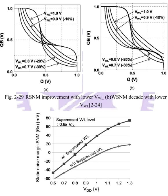
In order to improve cell stability, we can use another method which is the Dynamic Word-Line Level. The basic concept of the method is to use a higher Word-Line voltage to enhance the driving effect of the pass-gate n-type transistor, and then the write ability and read speed would be improved. But higher Word-Line voltage would increase the Read-Disturb voltage of the 6T SRAM cell which would decrease the Read Static Noise Margin (RSNM). Even the Half-selected Read Disturb issue would be more serious. In order to reduce the Read-Disturb voltage and the Half-selected Read Disturb, we can utilize the lower Word-Line voltage (such as Word-Line Under-Drive). Rather than adopt the higher Word-Line voltage, the driving effect of the pass-gate n-type transistor would be decrease. With the lower Word-Line voltage, the Read Static Noise Margin (RSNM) of all cells could be improved (Fig. 2-29(b)), and the Half-selected Read Disturb issue could be reduced. But the Write
33
Static Noise Margin (WSNM) would be decreased (Fig. 2-28). Hence, we can utilize these two dual supply skills to improve the read speed, the Read Static Noise Margin (RSNM) and the write ability. Fig. 2-30, Fig. 2-31, and Fig. 2-32 show the Multi-Step Word-Line technique [2-17, 2-18].
Fig. 2-29 RSNM improvement with lower VWL, (b)WSNM decade with lower
VWL[2-24]
34
Fig. 2-31 Boosting WL technique of the 6T SRAM [2-15]
Fig. 2-32 Multi-Step WL technique [2-17, 2-18]
2.5.4
Negative Bit-Line Level
Next, in order to improve the write ability, the Negative Bit-Line (NBL) is another method [2-19, 2-20, 2-21]. The basic concept is to use a boosting capacitor to couple a negative bias on Bit-Line into the storage node of cell to improve the write performance. If the Bit-Line voltage was lower than zero, the cross-couple pair latch could be easier enabled to flip the storage node data. So, this skill usually sets a negative voltage about -200mV at the Bit-Line to enhance the write ability and the Write Margin (WM). Although, from the Negative Bit-Line (NBL) skill, we can get many advantages that such as the Write Margin, the read speed and the write ability. If the implementation of the boosting capacitor uses the Metal-Insulator-Metal (MIM) structure, the cost will be increased. Rather than adopt the MOS capacitor, it is easier
35
to achieve, and not increase the cost. But, the MOS capacitor will increase the area overhead and the capacitance is unstable. So, we need to so consider impact to overall system area overhead when designing with this kind of skills. By the way, the Negative Bit-Line (NBL) scheme must have a very precisely timing control to maximize the improvement of write. Basically, the negative voltage should be generated before Word-Line turned on. But the timing is quite hard to be controlled and to be a crucial issue to the Negative Bit-Line (NBL). Fig. 2-32 and Fig. 2-33 show the Negative Bit-Line (NBL) scheme by using the boosting capacitor.
36
37
Chapter 3
Design of 1.0Mb 6T Pipeline
SRAM with Three Step-Up
Word-Line and Bit-Line Under
Drive and Adaptive Voltage
Detector skill
3.1 Introduction
In accordance with ITRS’s predictions, memory area will occupy nine-tenths area of the chip [3-1]. Static Random Access Memory (SRAM) is an important role, because it would dominate the area, performance, speed, die yield and power of the SOC chip. Besides, we know that high performance multi-core processors and clouding computing usually need high speed and large capacity SRAM to do data processing. However, with the reducing supply voltage and scaling process, the transistor characteristic variability would affect the subsistence of the standard SRAM in advance technology node. When the real chip was implemented, there must exist variation factor due to foundry makes the real physical device is different. The most common reasons are the systematic Global variation and Local random variations due to microscopic effects such as Random Doping Fluctuation (RDF) and Line Edge
38
Roughness (LER). So, with the technology node goes the deep sub-micron of process, these issues will become more serious than before the discussing.
When the SRAM cell is scaled, the cell stability, Static Noise Margin (SNM), and Vmin are limited by leakage, variation, and supply voltage. In order to facilitate
read and minimize Read-Disturb (VREAD) to make sure the cell won’t flip during read
operation, the designing of 6T SRAM must follow strong pull-down n-type transistor and weak pass-gate n-type transistor. And in order to improve write ability (write margin) during write operation, the designing of 6T SRAM must follow strong pass-gate n-type transistor and weak pull-up n-type transistor. But the read/write operation of 6T SRAM cell is conflicting. So, the optimization of 6T SRAM must consider the read/write requirements. Besides, in order to overcome these problems, several approaches have been proposed to reduce the leakage (sub-threshold leakage and gate leakage), variations (Vth variation, Global variation, and Local variation),
disturbs (Read-Disturb and Half-selected Disturb), etc. Such as using high-k metal technique, suppressing LER, optimizing channel profile, new device structure, read/write access circuits can reduce these issues [3-2~3-5].
In this work, we proposed a Variation-Tolerant Three Step-Up Word-Line (TSUWL) technique to improve the Read Static Noise Margin (RSNM), Write Static Noise Margin (WSNM), and read/write speed. We use the Step-Up Word-Line (previous design is called Word-Line Under-Drive (WLUD) [3-6 and 3-7]) scheme (SUWL) and Boosting Word-Line scheme [2-17 and 2-18] to form a Variation-Tolerant Three Step-Up Word-Line (TSUWL) technique. When the Word-Line signal is activated, the first step Word-Line voltage is lower about 90% of supply voltage that can reduce the Read-Disturb and Half-Selected Disturb issues. And the second step Word-Line voltage is pre-charge to original supply voltage that can avoid hurt the read speed and write ability. And the third step Word-Line voltage
39
is higher about increasing 200mV that can improve the read speed and write ability. During we use the Boosting Word-Line scheme, we propose an Adaptive Voltage Detector (AVD) reduce technique to avoid mitigate gate dielectric over-stress. Thin gate dielectric in deeply scaled technology such as EOT ≦ 1.8nm at 90nm, EOT ≈ 0.9nm at 32nm, and EOT ≈ 0.65-0.75nm at 22nm. So, the Gate Dielectric Reliability (GDR) must be considered. The basic concept of the Adaptive Voltage Detector is when voltage higher than designed voltage, the Booster will be not enabled; when voltage lower than designed voltage, the Booster will be enabled. We also propose another circuit technique “Bit-Line Under-Drive Read-Assist (BLUD)” to enhance read ability, Read Static Noise Margin (RSNM), and read speed. For read/write operation, before the Word-Line signal is activated, the Bit-Line voltage must be decreased about 30% of the supply voltage. However, it can reduce the Bit-Line loading to improve the Read Static Noise Margin (RSNM), read speed and no degradation of write ability, Write Margin (WM), and Write Vmin (previous design are
called Bit-Line Charge-Recycling (BLCR) [3-23] and Adaptive BL Bleeder [3-24]).Implemented the TSUWL and BLUD and AVD schemes in a 40nm 1.0Mb 6T SRAM with two stages Pipeline require 36.36% area overhead. This macro can operate across wide voltage range from 1.5V down to 0.6V, with operating frequency of [email protected] and 25oC. The remainder of this work is organized as follows. Section 3.2 presents Bit-Line Under-Drive (BLUD) Read-Assist scheme. Section 3.3 presents Three Step-Up Word-Line (TSUWL) Read/Write-Assist scheme. Section 3.4 presents Adaptive Voltage Detector (AVD) scheme. Section 3.5 presents the macro implementation and Post- Simulation result. Section 3.6 briefly introduces the test flow. Section 3.7 presents the measurement result of Test Chip.
40
3.2 Proposed Bit-Line Under-Drive (BLUD) Technique
With the scaling into the deep sub-micron of process, there many problems affect the subsistence of the 6T SRAM cell. However, at read operation, the 6T SRAM cell had a thorny problem which is Read-Disturb that would to hurt the original storage data (Fig. 3-1). The pass-gate n-type transistor (M3) and the pull-down n-type transistor (M2) form a voltage divider. In this case, we assume node “Q” is “0” (GND). When the signal of Word-Line goes high level, node “Q” would be rose to a voltage rather than ground voltage. And the rising voltage is called Read-Disturb that could decrease the Read Static Noise Margin (RSNM), even fail in read operation.
BL BLB WL VDD VDD Q QB
1
0
I
Read Disturb Voltage Vdisturb M1 M2 M3 M4 M5 M6 Vtrip
Fig. 3-1 Standard 6T SRAM cell schematic in Read mode
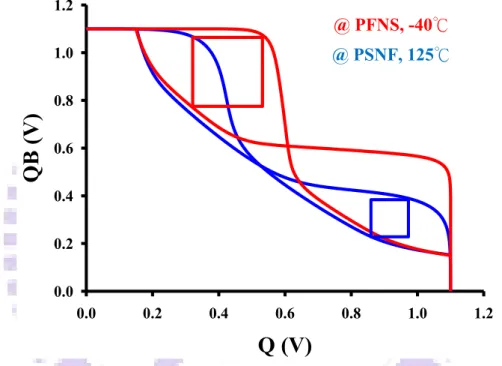
In read mode without Local Vth variation, the best case is at PFNS Global
variation and high temperature (125℃); the worst case is at PSNF Global variation and low temperature (-40℃). Compare best case with worst case on butterfly curve, the wing of the worst case is smaller than the best case. During at PSNF corner, all of
41
n-type transistors become stronger. So, the Read-Disturb voltage would increase and may to flip the trip voltage of opposite inverter. Fig. 3-2 shows the best case had larger square than the worst case. However, the most common seem problem to 6T SRAM Array is the Half-Selected Read Disturb issue. At the worst case, the Half-Selected Disturb will cause retention failure. Therefore, the first consideration of our methodology is to improve stability in read operation by improving the RSNM.
Q (V)
0.0 0.2 0.4 0.6 0.8 1.0 1.2Q
B
(V
)
0.0 0.2 0.4 0.6 0.8 1.0 1.2 @ PFNS, -40℃ @ PSNF, 125℃Fig. 3-2 Standard 6T SRAM cell butterfly curves under best and worst case In this work, we proposed a Variation-Tolerant Bit-Line Under-Drive (BLUD) technique to enhance SRAM stability for low-voltage operation, and improve Read Vmin. If the Bit-Line Under-Drive (BLUD) technique is achieved in dual supply
SRAM, the high cell supply (VCS) for cell stability and performance critical immediate neighboring circuits, and the low supply (VDD) for peripheral circuits to reduce power, and Word-Line connected to VCS for write ability tracks cell VCS. But the BLUD in dual supply SRAM had some disadvantages such as dual supply expensive, not suitable for cost-effective SRAM compiler applications (Fig. 3-3 ) [3-22].
42
Fig. 3-3 Bit-Line level in dual supply SRAM [3-22]
43
Fig. 3-4 shows the op-amp based push-pull Bit-Line voltage regulator. It can set Bit-Line level between 68%-78% of VDD to reduce the Read-Disturb voltage and Half-Selected Disturb. This technique had some advantages such as precise pining of Bit-Line level, PVT compensated design. But it still had some disadvantages such as Op-Amp (analog circuits, high supply voltage, area overhead, routing) not suitable for SRAM compiler applications (distributed SRAM macros with various sizes and configurations).
In this work, we used large signal sensing scheme (Fig. 3-6) for SRAMs with Bit-Line Under-Drive (BLUD) (Fig. 3-5) with following desired features: 1) Maintain the larger sense margin and better scalability of large signal single-ended sensing to enable further scaling, 2) Eliminate the leakage (hence possible sensing error) in large signal sensing with BLUD, 3) Simple implementation, 4) Minimum transistor count, 5) High-speed sensing, 6) Can be implemented in either single-supply or dual-supply SRAMs, 7) Easy implementation for SRAM compiler applications, 8) Variation tolerant. CLK SELE M0 M1 M2 M3 M4 M7 M8 M6 M5 PWR PC OSB<3> OSB<0:2> OSP<0:2> UD0 UD1 UD2 X3 X3 L B L _L O A D
44
Fig. 3-6 Large signal sensing circuit with Cross couple pair circuit
OSB<0> for Bit-Line discharge 40% of VDD, OSB<1> for Bit-Line discharge 30% of VDD, OSB<2> for Bit-Line discharge 20% of VDD, OSB<3> for no enable BLUD scheme; OSP<0> for setting BLUD level at 60% of VDD, OSP<1> for setting BLUD level at 70% of VDD, OSP<2> for setting BLUD level at 80% of VDD. SELE signal is selected bank signal; LXP is selected local word-line driver signal. Cross-coupled PMOS to develop full-rail signal, Complementary pre-charge PMOS/NMOS pair to neutralize coupling noise to LBL. Fig. 3-7 shows timing
L B L B L B L PCHP WL Q QB WL 16 Cells M3 M4 M6
Bit-Line Under Driver (BLUD) Power Circuit
Local Read Circuit
PCHN PCHN PC PWR M0 M1 M5 M2 PRESA
Cross Couple Pair Circuit
M7
M8 M9
RBL P1 M10
45
diagram for BLUD during read cycle. Assume OSB<1> and OSP<1> are high (Bit-Line discharge 30% of VDD and setting BLUD level at 70% of VDD). For read operation, if SELE goes high in the negative edge of CLK, PWR (Bit-Line power source) stars to discharge Bit-Line to desired level by M5, M6 (Fig. 3-5) and transmission gate (M2&M3 and M4&M5 (Fig.3-6)). Final the BLUD level set by M7&M8 voltage divider (Fig. 3-5). When positive edge of CLK comes and LXP goes high, (Local) Word-Line and cross couple pair will be activated to access the storage node data. For access “0”, the P1 signal can activate with Word-Line signal at the same time. But for access “1”, before the P1 signal is activated, the Bit-Line voltage must be at 90% of VDD. Due to we use PMOS to sense data with BLUD, if P1 is activated with Word-Line signal at the same time and Bit-Line level at 70% of VDD for access “1”, the read operation may fail. During Bit-Line level at 70% of VDD, the sensing PMOS is weakly activated that may to sense wrong data to Global Bit-Line.
CLK SELE PC UD0 UD1 UD2 LXP PCHN PCHP WL BL BLB PWR Q QB PRESA P1
46
Read Margin (RM) of the 6T SRAM cells can be defined as: RM=Vtrip – Vdisturb;
Where Vtrip represents the trip voltage of the inverter which is composed of a pull-up
p-type transistor and a pull-down n-type transistor. Fig. 3-8 shows the RM could be further improved if we adopt the BLUD technique. At supply 0.8V (PSNF @125℃) in read operation, the RM with BLUD technique has 31mV improvement. As supply voltage goes high, the improvement of RM is small than low supply voltage.
Supply Voltage (V)
0.8 0.9 1.0 1.1Read
Margin (mV)
0 50 100 150 200 250 300 W/O BLUD W/ BLUD @ 3 Sigma Improve 31mVFig. 3-8 The BLUD technique improves Read Margin with 3-σ variation
Fig. 3-9 shows the LBL falling time could be further reduced if we adopt the BLUD technique. At supply 0.8V (PSNF @125℃) in read “0” operation. The LBL falling time with BLUD technique has 104ps improvement. As supply voltage goes high, the improvement of LBL falling time is small than low supply voltage.
47
Supply Voltage (V)
0.8 0.9 1.0 1.1LB
L Fall
ing Time
(ps)
0 100 200 300 400 500 W/O BLUD W/ BLUD @ 3 Sigma Improve 104psFig. 3-9 The BLUD technique improves LBL falling time with 3-σ variation (read 0)
3.3 Proposed Three Step-Up Word-Line (TSUWL)
Technique
In recent years, there has been a dramatic increase research concerned with read/write access circuits. All of read/write access circuits were utilized to improve the RSNM, WSNM, read/write ability, and Vmin which such as Suppress Word-Line
supply, and Multi-Step Word-Line, Boosting Word-Line, Negative Bit-Line, etc. For Suppress Word-Line supply, it could reduce Read-Disturb and Half-Selected Disturb, but the read speed and write ability would be degraded due to the pass-gate n-type transistor would become weaker. Then, if we consider the Global variation at PSNF with high temperature (125℃) in Suppress Word-Line supply, the WSNM and read speed would suffer more serious degradation [3-6, 3-7, 3-8, 3-9, 3-10, 3-11]. Fig. 3-10 shows the RSNM increase with Suppress Word-Line supply. Fig. 3-11 shows the WSNM decrease with Suppress Word-Line supply.
48
Q (V)
0.0 0.2 0.4 0.6 0.8 1.0 1.2Q
B
(V
)
0.0 0.2 0.4 0.6 0.8 1.0 1.2@ PSNF, 125℃
V
WL= 1.1V
V
WL= 1.0V
V
WL= 0.9V
V
WL= 0.8V
V
WL= 0.7V
V
WL= 0.6V
Fig. 3-10 RSNM increase with suppress word-line supply
Q (V)
0.0 0.2 0.4 0.6 0.8 1.0 1.2Q
B (
V
)
0.0 0.2 0.4 0.6 0.8 1.0 1.2 @ PSNF, 125℃ VWL = 1.1V VWL = 1.0V VWL = 0.9V VWL = 0.8V VWL = 0.7V VWL = 0.6VWSNM curve have cross point (WSNM < 0) at VWL = 0.6V
![Fig. 2-11 The definition of the Write Margin (WM) [2-3]](https://thumb-ap.123doks.com/thumbv2/9libinfo/7494490.115699/24.892.158.748.121.895/fig-definition-write-margin-wm.webp)
![Fig. 2-15 SRAM critical path [2-5]](https://thumb-ap.123doks.com/thumbv2/9libinfo/7494490.115699/27.892.139.758.105.891/fig-sram-critical-path.webp)
![Fig. 2-20 The design of 11FO4 cycle time between cycle boundary [2-6]](https://thumb-ap.123doks.com/thumbv2/9libinfo/7494490.115699/33.892.139.757.113.869/fig-design-fo-cycle-time-cycle-boundary.webp)
![Fig. 2-31 Boosting WL technique of the 6T SRAM [2-15]](https://thumb-ap.123doks.com/thumbv2/9libinfo/7494490.115699/44.892.178.789.115.332/fig-boosting-wl-technique-t-sram.webp)