國 立 交 通 大 學
電子工程學系 電子研究所
碩 士 論 文
1.8伏金氧半低雜訊放大器之設計應用於超
寬頻UWB 3.1-10.6GH
Z
無線接收端
Design of a 1.8 -V CMOS LNA applied for
Ultra-Wideband 3.1 to 10.6GH
Z
Wireless
Receivers
研究生: 邱子倫
指導教授: 荊鳳德 博士
1.8伏金氧半低雜訊放大器之設計應用於超寬頻UWB
3.1-10.6GH
Z無線接收端
Design of a 1.8 -V CMOS LNA applied for
Ultra-Wideband 3.1 to 10.6GH
ZWireless Receivers
研 究 生:邱子倫 Student: Tzu-Lun Chiu
指導教授:荊鳳德 博士 Advisor: Dr. Albert Chin
國立交通大學
電子工程學系 電子研究所碩士班
碩士論文
A Thesis
Submitted to Department of Electronics Engineering & Institute of Electronics College of Electrical and Computer Engineering
National Chiao Tung University in Partial Fulfillment of the Requirements
for the Degree of Master
in
Electronics Engineering
June 2006
HsinChu, Taiwan, Republic of China
中華民國九十五年六月
I
1.8伏金氧半低雜訊放大器之設計應用於超
寬頻UWB 3.1-10.6GH
Z
無線接收端
學生: 邱子倫
指導教授: 荊鳳德 博士
國立交通大學
電子工程學系電子研究所
摘要
本論文研製一個應用於超寬頻 3.1-10.6 GHZ的低雜訊放大器。本研究 是以 0.18 微米互補式金氧半製程實現。此低雜訊放大器是以共源極和共閘極疊 接為放大器主架構,在共源極電晶體的閘極和源極兩端外加電容,在不增加電晶 體的大小下,補足濾波器所需電容值,達到低功率消耗的設計原則,並用一電容 與源極電感並聯,能減少源極電感對高頻響應的降低,用三階帶通柴比雪夫濾波 器做輸入匹配,而在輸出端是用共汲極電壓緩衝器做匹配,為了能在所應用的頻 段內達到相對的平坦增益,在疊接放大器中利用 shunt peaking 的方法去實現。 供應電壓 VDD為 1.8 伏特時,整個電路功率消耗約為 18mW,及包含 pad 的情況下 整個電路大小約為 0.992 mm2 。本研究的低雜訊放大器所量測的規格,順向增益 (S21)在 3.1-10.6GHz 時為 6dB-9.7dB,逆向隔離(S12)為-20dB 以下,S11 平均為 -7dB 以下,S22 平均為-10dB 以下,平均雜訊指數為 7dB,而線性度參數 IIP3 為 6dBm。Design of a 1.8 -V CMOS LNA applied for
Ultra-Wideband 3.1 to 10.6GH
Z
Wireless
Receivers
Student:
Tzu-Lun
Chiu
Advisor:
Dr.
Albert
Chin
Department of Electronics Engineering & Institute of Electronics
Nation Chiao Tung University
Abstract
A low noise amplifier is applied for ultra-wideband. This research is fabricated in 0.18-μm CMOS process. The three-order band-pass Chebyshev filter can reach the broadband input impedance matching. Owing to the low power consideration, plus the additional gate capacitor C . The cacoded structure gain stage provides the gain p
of the amplifier. The capacitor C reduces the gain degradation caused by s L at s
high frequency. The inductive shunt peaking maintain the gain flatness. Output buffer is used for output broadband matching. The low noise amplifier introduces the shunt peaking to achieve the flat gain purpose. The total power dissipation of the chip is about 18 mW at power supply 1.8 volt. The chip size included pad is 0.992 mm2. The
measurement result of this study expect that the forward gain S21 is 6 to 9.7dB at
3.1-10.6GHz, the reverse isolation S12 is under -20dB, the average S11 is under -7 dB,
III
誌 謝
謹向指導老師 荊鳳德 教授致上最大謝意,老師對研
究的熱誠態度影響了實驗室的每個同學,在老師的指導下,
也讓本篇論文得以順利完成。
還要感謝張慈學長、秋峰學長在研究和晶片量測上給
予的寶貴建議和幫忙,使的我的碩士論文得以完善。也要感
謝軍宏學長供應"精神"上的支援、建宏學長提供生活上的
所需、彬舫學長滿足我對咖啡的需求、存甫學長傳授海水魚
知識,還有同屆的肌肉猛男鴻瑋、胞兄弟國慶、魔獸達人科
閔、好鬼才達道,在研究方面有討論的同伴,及實驗室的大
家,讓我度過充實又愉快的碩班生活。
最後要感謝我的父母,致上最深的敬意,感謝他們對
我的栽培,不斷的在成長的路上鼓勵我,這一路上的支持,
才有今天的我。還有我的女友依廷小美仔,是我最大的精神
支柱,在我心情鬱悶時,總是及時的給我打氣加油,使我能
支撐下去,讓我有完成碩士學業的動力。
CONTENTS
ABSTRACT (CHINESE) ... I
ABSTRACT (ENGLISH) ...II
ACKNOWLEDGEMENTS ... III
CONTENTS ... IV
TABLE CAPTIONS...VII
FIGURE CAPTIONS ...VII
CHAPTER 1 Introduction ...1
1.1 Motivation ... 1
1.2 Thesis Organization ... 2
CHAPTER 2 Basic Concepts in RF Design...3
2.1 Receiver Architecture ... 3
2.1.1 Homodyne Receiver
...3
2.1.2 Heterodyne Receiver
...4
2.2 Linearity Basic... 6
2.3 Noise Basic ... 9
2.3.1 Noise Source ...10
2.3.2 Noise Model of MOSFET...11
V
CHAPTER 3 General Consideration in LNA Circuit
Design ...14
3.1 Low Noise Amplifier Basic ... 14
3.1.1 Impedance Matching Network...15
3.1.2 Stability………...16
3.1.3 Low Noise Amplifier Architecture Analysis …………..18
3.1.4 Optimizations of Low Noise Amplifier Design Flow...21
3.2 Broadband LNA introductions... 23
CHAPTER 4 Ultra-Wideband CMOS Low Noise
Amplifier Design ...28
4.1 Circuit topology and Design Consideration... 28
4.1.1 Input and output impedance matching network...29
4.1.2 Gain stage and Inductive Peaking...34
4.2 Chip Implementation and Measured Result... 38
4.2.1 Circuit Implementations...38
4.2.2 Experimental Results ...39
4.3 Comparison with no output buffer UWB LNA ... 47
CHAPTER 5 Summary ...50
VII
Table Captions
Table 4.1. Summary of simulated and measured results of UWB LNA. Table 5.1 Comparison of broadband LNA performance.
Figure Captions
Chapter 1 Introduction
Chapter 2 Basic Concepts in RF Design
Figure 2-1 Simple homodyne receiver architecture. Figure 2-2 Simple heterodyne receiver architecture.
Figure 2-3 Rejection of image versus suppression of interferers.
Figure 2-4 (a) Growth of output components in an intermodulation test (b) Intermodulation distortion.
Figure 2-5 A standard noise model of MOSFET.
Chapter 3 General Consideration in LNA Circuit Design
Figure 3-1 Common-source input stage with inductive source degeneration. Figure 3-2 Circuit embedded in a 50 ohm system.
Figure 3-4 Stability of two-port networks.
Figure 3-5 Equivalent noise model of Figure 3-1. Figure 3-6 Wide-band LNA circuit schematic.
Figure 3-7 Schematic circuit diagram of the cascade distributed amplifier. Figure 3-8 A de-embedded m-derivedπ-equivalent.
Chapter 4 Ultra-Wideband CMOS Low Noise Amplifier
Design
Figure 4-1 Circuit schematic of the UWB LNA. Figure 4-2 Third-order Chebyshev filter.
Figure 4-3 Input impedance approximation of the source degeneration LNA. Figure 4-4 Input impedance of the UWB LNA.
Figure 4-5 Output voltage buffer of the UWB LNA.
Figure 4-6 Gain stage and shunt peaking of the UWB LNA. Figure 4-7 The model of the shunt peaking amplifier. Figure 4-8 The layout diagram of the UWB LNA. Figure 4-9 The microphotograph of the UWB LNA. Figure 4-10 S11 simulated and measured result. Figure 4-11 S22 simulated and measured result.
IX
Figure 4-12 S21 simulated and measured result. Figure 4-13 S12 simulated and measured result. Figure 4-14 NF simulated and measured result. Figure 4-15 IIP3 simulated result.
Figure 4-16 IIP3 measured result.
Figure 4-17 Circuit schematic of the no output buffer UWB LNA.
Figure 4-18 Simulated S21 comparison between with buffer and no buffer LNA. Figure 4-19 Simulated NF comparison between with buffer and no buffer LNA. Figure 4-20 The layout diagram of the no buffer LNA.
CHAPTER 1
Introduction
_____________________________________________
1.1 Motivation
Recently , commercial wireless communication systems at gigahertz frequencies have been expanded extensively. Due to the advancement of integrated circuit design technology, circuit size is miniaturized and cost down considerations. Therefore, CMOS technology is attractive due to its advantages of high-level integration, low cost, and enhancing performance by scaling. The prospect of a single chip CMOS system has received considerable interest. Although the SOC is hard to implement at this moment, but a set of separating chips in the same CMOS technology may bring significant economic profit.
The interest in Ultra-wideband (UWB) system for wireless communication application has increased significantly. The US Federal Communications Commission (FCC) approval of UWB has prompted the IEEE 802.15.3a standards committee to establish a new physical layer standard utilizing the frequency spectrum from 3.1-GHz to 10.6GHz for consumer electronics applications. One of the proposed leading standards for UWB spectrum allocation is a multi-band with frequency hopping between these bands. The UWB frequency band is divided into several
2
sub-bands and each bandwidth has 528MHz. The modulation scheme is Multi band-OFDM [6]. Main application of UWB is short distance about 10 meters and high-speed wireless communication. UWB has very high data rate from 110M to 480M bps (bit per second). Otherwise, another advantage of UWB is the low power consumption.
The direct down-conversion receiver becomes more attractive since it has the advantages of low power, low complexity, and less extra components. And it lets system-on-chip (SOC) become possible. Typical, the first stage of the receiver is a low noise amplifier (LNA), which provides high gain and low noise to suppress the overall system’s noise performance. To implement the broadband LNA is the main object of this thesis.
1.2 Thesis Organization
The chapter 2 presents the basic concepts of RF design. These basic concepts which include the introduction of receiver architecture, linearity and noise provide the guidance for RF circuit design. The chapter 3 discusses the basic low-noise amplifiers design for UWB and other broadband amplifiers. In the chapter 4, a UWB LNA with wideband input matching network by using third-order Chebyshev filter is designed. Measurement result of the LNA chip fabricated by TSMC 0.18um CMOS technology is discussed. In the chapter 5, this work is summarized and concluded.
CHAPTER 2
Basic Concepts in RF Design
2.1 Receiver Architecture
2.1.1 Homodyne Receiver
The homodyne receiver is also called “direct-conversion” or “zero-IF” architecture, since the RF signal is directly down-converted to the baseband in the first downconversion. In the homodyne receiver, the LO frequency is equal to the input carrier frequency, and channel selection requires only a low-pass filter with relatively sharp cutoff characteristics. The simple homodyne architecture is shown in Figure 2-1. But quadrature outputs are needed for frequency and phase-modulated signals, since the two sides of FM or QPSK spectra carry different information. In recent years, this architecture becomes the topic of active research gradually due to the following reasons:
(1) The problem of image is removed due to 0
IF
ω = . Therefore no image filter is required, and the LNA need not drive a 50-ohm load.
(2) It is attractive for monolithic integration because this architecture needs less external components.
4
design. But some extra issues that do not exist or are not as serious in a heterodyne receiver must be entailed, such as channel selection, DC offset, I/Q mismatch, even-order distortion, and flicker noise.
2.1.2 Heterodyne Receiver
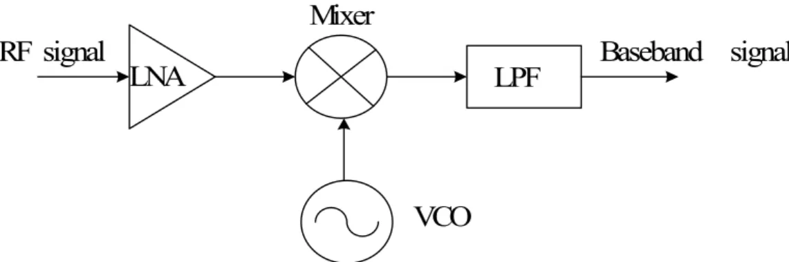
In heterodyne architectures, the signal band is translated into much lower frequencies by down-conversion mixer, and the filters are used to select the band and channel of the interested signals. In general, the low noise amplifier is placed in front of the down-conversion mixer, since the noise of the down-conversion mixer is high. A simple heterodyne architecture is shown in Figure 2-2.This architecture is the most reliable reception technique today. But if the cost, complexity, integration and power dissipation are the primary criteria, the heterodyne receiver will become unsuitable due to its complexity and the need for a large number of external components.
LNA
Mixer
LPF
VCO
signal
RF
Baseband
signal
Frequency planning is an important thing in heterodyne receiver. For high-side injection, an undesired signal (image) at a frequency of ωIM =ωLO +(ωLO −ωRF )
is translated into the same frequency, intermediate frequency (IF), as the desired signal. Similarly, for low-side injection, the image frequency is at
)
( RF LO
LO
IM ω ω ω
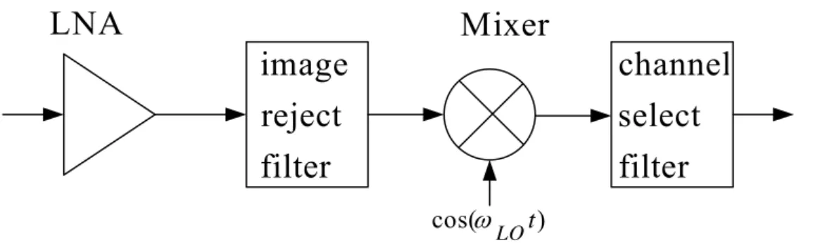
ω = − − . Therefore the image would cause the distortion of the signal at the intermediate frequency. As shown in Figure 2-3, some techniques are necessary to suppress the image, such as image reject filter. How to choose the intermediate frequency? If 2ωIF is sufficiently large, the image reject filter will have a relatively small loss in the signal band and a large attenuation in the image band. But a lower 2ωIF will release the quality factor of the channel select filter to get great suppression of nearby interferers. Therefore we must take a trade-off between image rejection and channel selection.
) cos( t LO ω
Mixer
filter
reject
image
filter
select
channel
LNA
6 0 0
ω
ω
ω
ω
LO ω LO ω channel Desired channel Desired Interferer Interferer image image filter reject image filter reject image filter select channel filter select channel IF ω IF ω ) (a ) (b IM ω RF ωFigure 2-3 Rejection of image versus suppression of interferers.
2.2 Linearity Basic
The nonlinearity of the system often leads to interesting and important phenomena, such as harmonics, gain compression, desensitization, blocking, cross modulation, intermodulation, etc. These distortions will degrade the performance of the system.
When two signals with different frequencies are applied to a nonlinear system, the output exhibits some components that are not harmonics of the input frequencies in general. This is called intermodulation (IM), and this phenomenon arises from multiplication of the two signals when their sum is raised to a power greater than unity. We assume that
x
(
t
)
=
A
1cos
ω
1t
+
A
2cos
ω
2t
(2.1) Thus, 3 2 2 1 1 2 2 2 1 1 2 2 2 1 1 1)
cos
cos
(
3
)
cos
cos
(
)
cos
cos
(
)
(
t
A
t
A
t
A
t
A
t
A
t
A
t
y
ω
ω
α
ω
ω
α
ω
ω
α
+
+
+
+
+
=
(2.2) Expanding the left side and discarding DC terms and harmonics, we obtain the intermodulation products: t A A t A A ) 2 cos( 4 3 ) 2 cos( 4 3 : 2 2 1 2 2 1 3 2 1 2 2 1 3 2 1 ω ω α ω ω α ω ω ω → ± + + − (2.3) t A A t A A ) 2 cos( 4 3 ) 2 cos( 4 3 : 2 1 2 1 2 2 3 1 2 1 2 2 3 1 2ω
ω
α
ω
ω
α
ω
ω
ω
→ ± + + − (2.4)Furthermore, among the intermodulation products, the third-order intermodulation products at 2ω1−ω2 and 2ω2 −ω1 is important. Since if the difference between ω and 1 ω is small, the distortions at 2 2ω1−ω2 and 2ω2 −ω1
will appear in the vicinity of ω and 1 ω . 2
) ( ) , , ( 4 3 1 1 2 2 1 3 2 2 3 ω ω ω ω j H j j j H A IM = − (2.5)
This effect causes some distortion at our desired frequency and damages desired signals. Therefore third intercept point (IP3) is used to characterize this behavior. This parameter is measured by supplying a two-tone signal to the system. This input signal must be chosen to be sufficiently small in order to remove higher-order nonlinear terms. In a typical test, A1=A2=A, hence the magnitude of third-order intermodulation
8
products grows at three times the rate at which the fundamental signal on a logarithmic scale when input signal increases. The third-order intercept point is defined to be the point at which third-order intermodulation product equals to the fundamental signal, and the corresponding input signal is called input IP3 (IIP3) and the corresponding output signal is called output IP3 (OIP3). The AIP3, therefore, can
be obtained by setting IM3 =1 and expressing as
) , , ( ) ( 3 4 2 2 1 3 1 1 2 3 ω ω ω ω j j j H j H AIP − = (2.6)
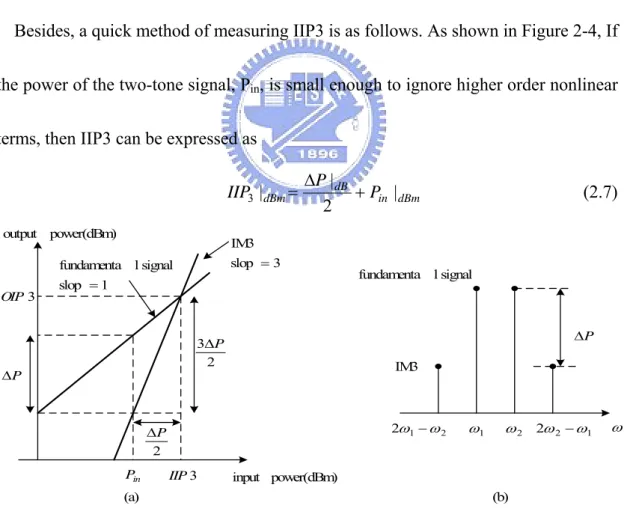
Besides, a quick method of measuring IIP3 is as follows. As shown in Figure 2-4, If the power of the two-tone signal, Pin, is small enough to ignore higher order nonlinear
terms, then IIP3 can be expressed as
dBm in dB dBm P P IIP | 2 | | 3 + Δ = (2.7) P Δ 2 P Δ 2 3 PΔ 3 IIP 3 OIP in P input power(dBm) power(dBm) output ω 1 ω ω2 2 1 2ω −ω 2ω2 −ω1 P Δ 1 slop signal l fundamenta = 3 slop IM3 = signal l fundamenta IM3 (a) (b)
Figure 2-4 (a) Growth of output components in an intermodulation test (b) Intermodulation distortion.
2.3 Noise Basic
Noise can be loosely defined as any random interference unrelated to the signal of interest, and noise is characterized by a PDF and a PSD. In analog circuits, the signal-to-noise ratio (SNR), defined as the ratio of the signal power to the total noise power, is an important parameter. But in RF design, most of the front-end receiver blocks are characterized in terms of their noise figure, which is a measure of SNR degradation due to the added noise from the circuit/system, rather than the input-referred noise. Noise factor can be expressed as
source input to due power noise output power noise output total factor noise = (2.8)
the noise figure (NF) is simply the noise factor expressed in decibels. If a system has no noise, then noise figure is 0 dB regardless of the gain. In reality, the finite noise of a system degrades the SNR, yielding noise figure > 0 dB. For those whose noise factor is quite close to unity, noise temperature, TN, is an alternative way of
expressing the effect of noise contribution due to its higher-resolution description of noise performance, and is defined as the increase in temperature required of the source resistance for it to account for all of the output noise at the reference temperature Tref (which is 290 K). It is related to the noise factor as follows:
1) -factor (noise T T T T 1 factor noise N ref ref N ⇒ = ⋅ + = (2.9)
10
2.3.1 Noise Source
Thermal noise:
Thermally agitated charge carriers in a conductor constitute a randomly varying current that gives rise to a random voltage due to their Brownian motion. Thermal noise is often called Johnson noise or Nyquist noise. The noise voltage has a zero average value, but a nonzero mean-square value.
In a resistor R, thermal noise can be represented by a series noise voltage source 2 4
n
v = kTR fΔ or by a shunt noise current source in2 4kT f R
Δ
= , where k is k is Boltzmann’s constant (about 1.38×10⁻²³ J/K), T is the absolute temperature in
Kelvins, and Δf is the noise bandwidth. However, purely reactive elements generate no thermal noise.
Shot Noise:
Shot noise occurs in PN junctions, and two conditions for shot noise to occur: (1) There must be direct current flow.
(2) There must be energy barrier over which a charge carrier hops.
Charge comes in discrete bundles. The randomness of the arrival time gives rise to the whiteness of shot noise. Therefore the shot noise can be modeled by a shunt noise current source 2 2
n DC
i = qI Δ , where q is the electronic charge, If DC is the DC current
Flicker Noise:
Flicker noise appears as 1/f character and is found in all active devices, as well as in some discrete passive element such as carbon resistors. In diodes, flicker noise is caused by traps associated with contamination and crystal defects in the depletion regions. The traps capture and release carriers in a random fashion and the time constants associated with the process give rise to the 1/f nature of the noise power density. The flicker noise in diode can be represented as 2
j j K I i f f A = ⋅ ⋅ Δ , where K is the process-dependent constant, Aj is the junction area, and I is the bias current. In
MOSFET, charge trapping phenomena are invoked in surface, and his type of noise is much greater than that of the bipolartransistor. The flicker noise in MOSFET can be given by 2 2 2 2 m n T ox g K K i f A f f WLC f ω = ⋅ ⋅ Δ ≈ ⋅ ⋅ ⋅ Δ (2.10) where K is the process-dependent constant, and A is the area of the gate.
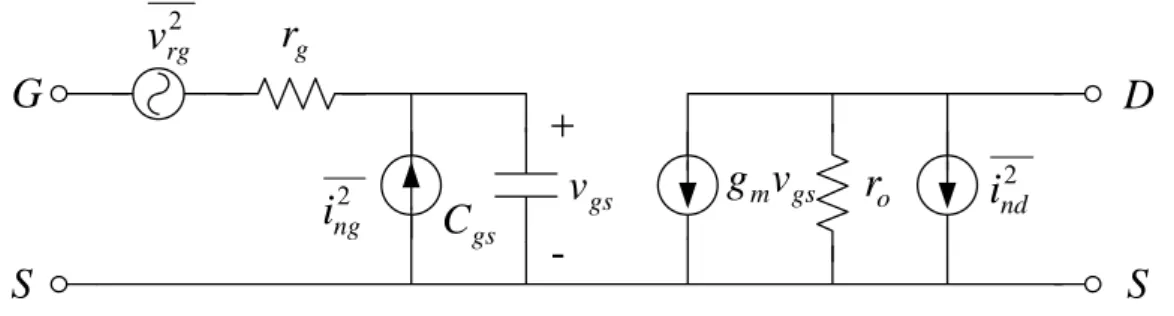
2.3.2 Noise Model of MOSFET
The dominant noise source in CMOS devices is channel noise, which basically is thermal noise originated from the voltage-controlled resistor mechanism of a MOSFET. This source of noise can be modeled as a shunt current source in the output circuit of the device. The channel noise of MOSFET is given by
f g kT
12
where γ is bias-dependent factor, and gd0 is the zero-bias drain conductance of the
device. Another source of drain noise is flicker noise and is given by equation 2.10. Hence, the total drain noise source is given by
f WLC g f K f g kT i ox m d nd = Δ + ⋅ 2 ⋅Δ 2 0 2 4 γ (2.12)
At RF frequencies, the thermal agitation of channel charge leads to a noisy gate current because the fluctuations in the channel charge induce a physical current in the gate terminal due to capacitive coupling. This source of noise can be modeled as a shunt current source between gate and source terminal with a shunt conductance gg,
and may be expressed as
f g kT ing =4 δ gΔ
2 (2.13)
where the parameter gg is shown as
0 2 2 5 d gs g g C g =ω (2.14)
and δ is the gate noise coefficient. This gate noise is partially correlated with the channel thermal noise because both noise currents stem from thermal fluctuations in the channel, and the magnitude of the correlation can be expressed as
j i i i i c d g d g 395 . 0 2 2 * ≈ ⋅ ⋅ ≡ (2.15)
where the value of 0.395j is exact for long channel devices. Hence, the gate noise can be re-expressed as
) | | 1 ( 4 | | 4 ) ( 2 2 2 2 c f g kT c f g kT i i ing = ngc + ngu = δ gΔ + δ gΔ − (2.16)
where the first term is correlated and the second term is uncorrelated to channel noise. From previous introduction of MOSFET noise source, a standard MOSFET noise model can be presented in Figure 2-5, where 2
nd
i is the drain noise source, ing2 is the
gate noise source, and 2
rg
v is thermal noise source of gate parasitic resistor r . g
2.3.3 Noise Figure of Cascaded Stages
For a cascade of m stages, the overall noise figure can be characterized by Friis formula ) 1 ( 1 2 1 1 ... 1 ) 1 ( 1 − − + + − + − + = m p m p total A NF A NF NF NF (2.17)
where NF is the noise figure of stage n, and n A denotes the power gain of pn
stage n. This equation indicates that the noise contributed by each stage decreases as the gain preceding the stage increases. Hence, the first few stages in a cascade are the most critical for noise figure. But if a stage exhibits attenuation, then the noise figure of the following circuit is amplified when referred to the input of that stage [5].
G
S
gsC
D
S
2 ngi
v
gsg
mv
gsr
oi
nd2 2 rgv
r
g-+
14
CHAPTER 3
General Consideration in LNA Circuit Design
_____________________________________________
3.1 Low Noise Amplifier Basic
Low noise amplifier is the first gain stage in the receive path so its noise figure directly adds to that of the system. Therefore, there are several common goals in the design of LNA. These include minimizing noise figure of the amplifier, providing enough gain with sufficient linearity and providing a stable 50 ohm input impedance to terminate an unknown length of transmission line which delivers signal from antenna to the amplifier [9]. Among LNA architectures, inductive source degeneration is the most popular method since it can achieve noise and power matching simultaneously, as shown in Figure 3-1. The following analysis after 3.1.3 is based on this architecture. The LNA basic considerations are introduced as follows.
in Z s L g L 1 M
3.1.1 Impedance Matching Network
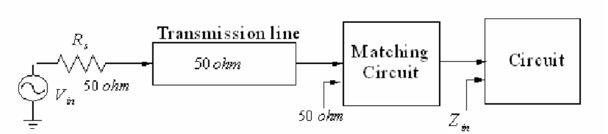
The need for impedance matching network becomes more important. In order to deliver maximum power to a load, must be properly terminated at both the input and the output ports. The input impedance of a circuit can be any values. In order to have the best power transfer into the circuit, it is necessary to match this impedance to the impedance of the source driving the circuit. The output impedance must be similarly matched. In order to deliver maximum power to the 50 ohm load, must have the terminations ZS and ZL. The input matching network is designed to transforms the
generator impedance to the source impedance ZS, and the output matching network
transforms the 50 ohm termination to the load impedance ZL. Consider the RF system
shown in Figure 3-2. Here the source and load terminations are 50ohm, as are the transmission lines leading up to the circuit for optimum power transfer, prevention of ringing and radiation, and good noise behavior. For example, we needs the circuit input and output impedances matched to the system. In general, some matching circuit must almost always be added to the circuit, as shown in Figure 3-3. Typically, reactive matching circuits are used because they are lossless and because they do not add noise to the circuit. Note that, in general, when an impedance is complex
(
R+ jX)
. Then to16
Figure 3-2 Circuit embedded in a 50 ohm system.
Figure 3-3 Circuit embedded in a 50 ohm system with matching circuit.
3.1.2 Stability
The stability of an amplifier is a very important consideration in a design and can be determined from the S parameters, the matching networks, and the terminations. A two-port network to be unconditionally stable can be derived from (3.1) to (3.4).
1
<
Γ
s (3.1)1
<
Γ
L (3.2)1
1
22 1 2 2 1 11−
Γ
<
Γ
+
=
Γ
L L N IS
S
S
S
(3.3)1
1
11 1 2 2 1 22<
Γ
−
Γ
+
=
Γ
S s OUTS
S
S
S
(3.4)The two-port network is shown in Figure 3-4. For unconditional stability any passive load or source in the network must produce a stable condition. The solution of (3.1) to (3.4) gives the required conditions for the two-port network to be unconditionally stable. [4] 21 2 1 2 2 2 2 2 11
2
1
S
S
S
S
k
=
−
−
+
Δ
(3.5) 21 12 22 11S
S
S
S
−
=
Δ
(3.6) A convenient way of expressing the necessary and sufficient conditions for unconditional stability is1
>
k
(3.7)1
<
Δ
(3.8)E
SZ
sΓ
sΓ
I NZ
I NT w o - p o r t
n e tw o r k
O U TΓ
LΓ
Z
O U TZ
LFigure 3-4 Stability of two-port networks.
18
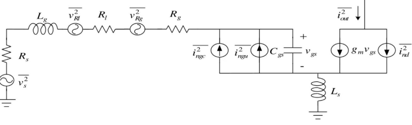
In Figure 3-5, the input impedance can be expressed as
gs s g o s T s gs m s gs m gs s g in C L L at L L C g L C g sC L L s Z ) ( 1 1 ) ( + = = ≈ ⎟ ⎟ ⎠ ⎞ ⎜ ⎜ ⎝ ⎛ = ⎟ ⎟ ⎠ ⎞ ⎜ ⎜ ⎝ ⎛ + + + = ω ω ω (3.9)
as shown in equation (3.9), the input impedance is equal to the multiplication of cutoff frequency of the device and source inductance at resonant frequency. Therefore it can be set to 50 ohm for input matching while resonant frequency is designed to be equal to the operating frequency.
According to prior introduction, the equivalent noise model of common-source LNA with inductive source degeneration can be expressed as Figure 3-5, where R is l
the parasitic resistance of the inductor, R is the gate resistance of the device. Note g
that the overlap capacitance Cgd has also been neglected in the interest of simplicity.
Then the noise figure can be obtained by computing the total output noise power and output noise power due to input source. To find the output noise, we first evaluate the trans-conductance of the input stage. With the output current proportional to the voltage no Cgs and noting that the input circuit takes the form of series-resonant
network, the transconductance at the resonant frequency can be expressed as
s o T s T s gs o m in m m R L R C g Q g G ω ω ω ω ( + ) = 2 = = (3.10)
gs C 2 ngu i vgs gmvgs ind2 2 Rg v -+ 2 ngc i g R l R g L s L s R 2 Rl v 2 s v 2 out i
Figure 3-5 Equivalent noise model of Figure 3-1.
where Qin is the effective Q of the amplifier input circuit. So the output noise power
density due to the source can be expressed as
2 2 2 2 . , ) 1 ( 4 ) ( s s T s o T eff m Rs o Rs a R L R kT G S S ω ω ω ω + = = (3.11)
In the similar way, the output noise power density due to Rg and Rl is
2 2 2 2 , , ) 1 ( ) ( 4 ) ( s s T s o T l g o R R a R L R R R kT S l g ω ω ω ω + + = (3.12)
Furthermore, channel current noise of the device is the dominant noise contributor, and its noise power density associated with the correlated portion of the gate noise can be expressed as
2 , , ) 1 ( 4 ) ( s s T do o i i a R L g kT S ngc nd ω γκ ω + = (3.13)
where γ is the coefficient of channel thermal noise, α = gm/gd0 and 2 2 2 5 2 1 5 ⎥⎦ ⎤ ⎢ ⎣ ⎡ + + = γ δα γ δα κ c cQL (3.14)
20 gs s o L C R Q ω 1 = (3.15)
The last noise term is the contribution of the uncorrelated portion of the gate noise, and its output noise power density can be expressed as
2 , ) 1 ( 4 ) ( s s T do o i a R L g kT S ngu ω γξ ω + = (3.16) where ) 1 )( 1 ( 5 2 2 2 L Q c + − = γ δα ξ (3.17)
According to equations (3.11), (3.12), (3.13) and (3.16), the noise figure at the resonant frequency can be expressed as
⎟⎟ ⎠ ⎞ ⎜⎜ ⎝ ⎛ + + + = T o L s g s l Q R R R R F ω ω α γχ 1 (3.18) where ) 1 ( 5 5 | | 2 1 2 2 2 L L Q Q c + + + = γ δα γ δα χ (3.19)
From equation (3.19), we observe that χ includes the terms which are constant, proportional to QL, and proportional to QL2. It follows that equation (3.19)
will contain terms which are proportional to QL as well as inversely proportional to
L
3.1.4 Optimizations of Low Noise Amplifier Design Flow
The analysis of the previous section can now be drawn upon in designing the
LNA. In order to pick the appropriate device size and bias point to optimize noise performance given specific objectives for gain and power dissipation, a simple second-order model of the MOSFET transconductance can be employed which accounts for high-field effects in short channel devices. Assume that the drain current, Id, has the form
ρ ρ + = − + − = 1 1 ) ( 2 sat sat ox T gs sat T gs sat ox DS WC v LE V V LE V V v WC I (3.20) where sat T gs LE V V − ≡
ρ . And the equation (3.15) can be replace as
WL Q R C R WLC Q o L s ox s ox o L ω ω 2 3 2 3 ⇒ = = (3.21)
The power consumption of the LNA, therefore, can be expressed as
ρ ρ ω + = = 1 1 2 3 2 sat sat o s L DD DS DD D v E R Q V I V P (3.22)
The noise figure can be expressed in terms of PD and Vgs. Two parameters linked to
power dissipation need to be accounted for.
) ( 1 gs gs m T f V C g = ≈ ω (3.23) ) , ( 1 1 2 3 2 2 2 D gs D o s o D sat sat DD L f V P P P R P E v V Q = + = + = ρ ρ ρ ρ ω (3.24)
22 where s o sat sat DD o R E v V P ω 2 3 = .
The noise figure of the LNA, therefore, can be expressed as
) , ( ) 1 ( 5 5 | | 2 1 1 2 2 2 D gs L L T o L s g s l P V f Q Q c Q R R R R F ⎟⎟= ⎠ ⎞ ⎜ ⎜ ⎝ ⎛ + + + ⎟⎟ ⎠ ⎞ ⎜⎜ ⎝ ⎛ + + + = γ δα γ δα ω ω α γ (3.25)
In general, there are two approaches to optimize noise figure. The first approach assumes a fixed transconductance, Gm. The second approach assumes fixed
power consumption.
(1) Fixed Gm optimization: To fix the value of the transconductance, Gm, we need
only assign a constant value to ρ. Once ρ is determined, the optimization of the noise figure can be obtained by equation (3.25):
) , ( 0 ) , ( . .
.opt Lopt gs Dopt D Vgs fixed D D gs P V f F Q P P P V f = ⇒ ⇒ ⇒ = ∂ ∂ (3.26)
From equation (3.21), we can obtain the optimal width to get the minimal noise figure for a given Gm under the assumption of matched input impedance. In this
approach, the designer can achieve high gain and low noise performance by selecting the desired transconductance, but its disadvantage is that we must sacrifice the power consumption to achieve minimum noise figure.
(2) Fixed PD optimization: An alternative method of optimization fixes the power
dissipation and adjusts device size and bias point to minimize the noise figure. Once PD is determined, the optimization of the noise figure can be obtained by
equation (3.27): ) , ( 0 ) , ( . .
.opt Lopt gsopt D gs P fixed gs D gs P V f F Q V V P V f D = ⇒ ⇒ ⇒ = ∂ ∂ (3.27)
Then the optimum device size can be obtained to get the best noise performance for fixed power dissipation. In this approach, the designer can specify the power dissipation and find the optimal noise performance, but its disadvantage is that the transconductance is held up by the optimal noise condition [5].
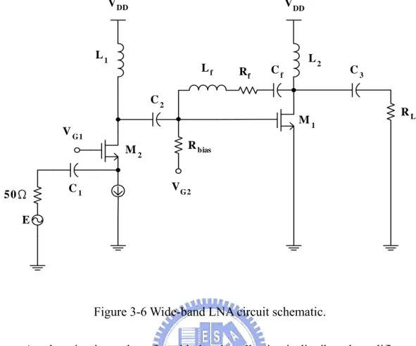
3.2 Broadband LNA introductions
Figure 3-6 is the LNA circuit schematic. We discuss this circuit step by step from the first stage. First, to make1/gm =50ohm, the gm value of common gate
amplifier is going to be fixed at certain trans-conductance. An additional stage is required to provide sufficient gain over the desired band. A shunt feedback common source amplifier is used in the second stage for this purpose. The first step is the selection of transistor size and bias condition of the M1 to yield
ohm g
Z 1/ m 50
Re 11 = = . This ensures input matching condition for wide-band of frequency. But this condition is violated with optimum noise condition. There is a trade-off between noise and impedance matching in the LNA circuit. One of the major problems in the wide bandwidth amplifier design is the limitation imposed by the gain-bandwidth product of the active device. We know that any active device has a
24
gain roll off at high frequency because of the gate-drain and gate-source capacitance in the transistor. This effect degrades the forward gain as the frequency increases and eventually the transistor stops functioning as an amplifier at the high frequency. Therefore the second design step is the selection of optimal bias point of second stage of LNA so that it operates at its maximum fT. In addition to this S21 degradation
with frequency other complications that arises in wide-bandwidth amplifier design includes, increase in reverse gain S12 and noise figure at high frequency. Negative
feedback configuration is used to reduce these effects and increase the bandwidth. An inductor L is connected in series with Rf such that after certain frequency the negative
feedback decreases in proportion to the S21 roll-off. This technique improves gain
flatness at high frequency. The load inductance of L1 and L2 replace the resistor load
which is used conventionally. The magnitude of the inductor’s impedance increases as frequency increases. This increase inductor impedance compensates the active device gain degradation that occurs at high frequency [10].
E VDD VDD VG1 VG2 M2 M1 50Ω C1 C2 Cf C3 Rbias Rf Lf L1 L 2 RL
Figure 3-6 Wide-band LNA circuit schematic.
Another circuit topology for wide-band application is distributed amplifier (DA). Distributed amplifier was first introduced by [17]. MMIC DA was mainly implemented using GaAs-based or SiGe devices. The distributed amplifier schematic is
shown in Fig. 3-7. From the Fig. 3-7, we can observe that the power gain of a cascade pair is considerably higher than that of a common-source single transistor. The input signal propagates down the gate line, with each FET tapping off some of the input power. The amplified output signals from the FETs form a traveling wave on the drain line. The propagation constants and lengths of the gate and drain lines are chosen for constructive phasing of the output signals, and the termination impedanc3es on the lines serve to absorb waves traveling in the reverse directions. According to
26
equivalent circuit of a single unit cell of the gate line and drain line, we can get optimal number of section [3].
d d g g d d g g opt l l l l N α α α α − =ln( / ) (3.28)
A small resistor Rgx is added in the gate of common-gate transistor to improve
the entire circuit stability. The input and output impedances of the cascade device are needed. In the DA design, the input and output of the cascade FETs used in the distributed amplifier were terminated by the gate line characteristic impedance Zog
and drain line characteristic impedance Zod, respectively. Higher gain can be obtained
by choosing higher characteristic impedance of gate (Zog) and drain lines (Zod) but the
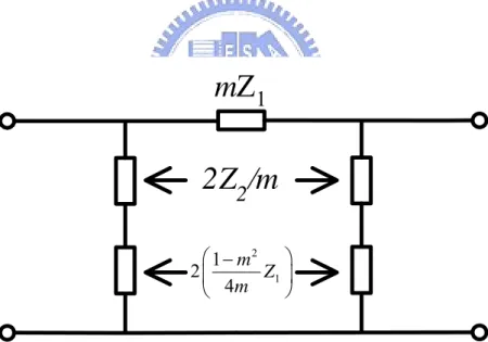
cutoff frequency will be lower, which will limit the bandwidth. The m-derived matching section is used in our design to overcome the well-known non-constant image impedance from the constant-k sections. A de-embedded m-derived π
equivalent circuit is shown in Fig. 3-8. Distributed amplifiers are not capable of very high gains or very low noise figure, however, and generally are larger in size than an amplifier having comparable gain over a narrower bandwidth.
V
DDV
G1V
G2Output
Input
M-Derived matching
section
Rgx Rgx RgxFig. 3-7. Schematic circuit diagram of the cascade distributed amplifier.
2Z
2
/m
2 1 1 2 4 m Z m ⎛ − ⎞ ⎜ ⎟ ⎝ ⎠mZ
1
28
CHAPTER 4
Ultra-Wideband CMOS Low Noise Amplifier Design
_____________________________________________
4.1 Circuit topology and Design Consideration
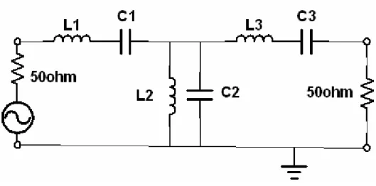
We use the three-order band-pass Chebyshev filter to maintain the flat gain at the Ultra Wide-band operating frequency spectrum from 3.1 to 10.6 GHz. Figure 4-1 shows the whole proposed ultra-wideband CMOS LNA circuit schematic. The input impedance Z is embedded in a three-order band-pass Chebyshev filter to resonate in
its image part over the entire band. To add flexibility to the design, an inductor (L ) g
is placed in series with the gate, and a capacitor (C ) is placed in parallel with the p
gate source of the input device. A capacitor (C ) is placed in parallel with the source s
degeneration inductor (L ). The gain stage is cascode structure (s M1, M2) which
improves the reverse isolation and provides the frequency response of the amplifier. The Ultra-wideband is for 3.1 to 10.6 GHZ application. The flat forward gain over
the whole bandwidth is essential. A technique that satisfied this requirement of large bandwidth at low cost is known as inductive peaking. The resistance Rd improves the
gain at lower frequency. At high frequency, the Ld can maintain the gain.
Source-follower voltage buffer (M ) is intended to drive an external 50 ohm load. It 3
Figure 4-1 Circuit schematic of the UWB LNA.
4.1.1 Input and output impedance matching network
Figure 4-2 is the third-order band-pass Chebyshev filter. Design a band-pass filter having a 0.5 dB equal-ripple response, with three order (N=3) [3]. The center frequency is 5.7 GHz. The termination is 50 ohm. The four parameters g1, g2, g3, g4, are the prototype element values by definition. The reactive devices L1, C1, L2, C2, L3, C3 (C3 =Cgs1+Cp, in the next discussion, C is divided into 3 Cgs1 and Cp ),
are the components of the third-order band-pass Chebyshev filter. ωb is the beginning frequency, and ωc is the cutoff frequency, and ωo is the center frequency. Design flow is as follows. The first thing is choosing the beginning
30
frequency (ωb) and cutoff frequency (ωc), then knows the bandwidth and center frequency (ωo). Second, we can know the prototype element values g1, g2, g3, g4, from the choosing numbers of ripples and stages. Finally, put the values in the equations (4.1) of L1, C1, L2, C2, L3, C3, and we can get the values of the components we want. L
R
g
L
g
C
g
L
g
1=
1′
,
2=
2′
,
3=
3′
,
4=
c b o o b cfreq
center
BW
ω
ω
ω
ω
ω
ω
⋅
=
−
=
Δ
,
.)
(
)
(
o o o o o o o o o o o oZ
L
C
Z
L
L
Z
C
C
C
Z
L
Z
L
C
Z
L
L
⋅
′
⋅
Δ
=
Δ
⋅
⋅
′
=
⋅
Δ
⋅
′
=
′
⋅
⋅
Δ
=
⋅
′
⋅
Δ
=
Δ
⋅
⋅
′
=
3 3 3 3 2 2 2 2 1 1 1 1ω
ω
ω
ω
ω
ω
(4.1)Figure 4-2 Third-order Chebyshev filter.
The input impedance (Zi) of the transistor with inductive source degeneration is a series RLC circuit. The equation (4.2) is Zi. The real part of Zi is chosen to be equal to source resister (filter termination), that is ωTLs = Rs. If the two image part of Zi
can cancel each other, the input impedance can match Rs. In the filter passband, the power loss is 0 dB, with a ripple ρp. The choice of reactive elements in the filter
determines the bandwidth and the in-band ripple. The input reflection coefficient Γ is related to ρp by p ρ 1 1 2 − =
Γ [12]. Use the filter to let ρp =1, then Γ2 =0. The filter can achieve the input broadband impedance matching. Figure 4-3 shows the input impedance approximation of the source degeneration LNA.
)
(
1
)
(
)
)(
(
)
(
)
(
1
)
(
1 1 2 1 s p gs s p gs s T s p gs g s s T g s s p gs iC
C
C
s
C
C
C
L
s
C
C
C
L
L
s
L
L
L
s
C
C
C
s
s
Z
+
+
+
+
+
+
+
+
+
=
+
+
+
+
+
≅
ω
ω
(4.2)32
Figure 4-3 Input impedance approximation of the source degeneration LNA.
In the Figure 4-4, it shows the input impedance of the Ultra-Wideband LNA. Equation (4.3) has the detail derivation of the whole input impedance. Z1 is the
impedance of L1, C1 series. Z2 is the impedance of L2, C2 parallel. Z is other 3
impedance of original source degeneration LNA, and is similar to Zi. Z is the in
combination of the three part impedance. ω is the 3dB cutoff frequency. T
The noise resistance and minimum noise figure are not effected by the addition of C . For low-power design, where p Cgs1 of transistor is small, the
required degeneration inductance L can be reduced by the addition of s C [13]. p
This way can increase capacitance without raising the transistor size, and it can procure the low-power purpose. At dc frequency, L provides the dc ground. As s
frequency increasing, the impedance of L degrades the frequency respond, and s
s
C which reduces the gain degradation caused by L provides ac ground at s
)
(
,
)
1
//
1
(
)
1
//
(
,
1
//
,
1
)
(
)
(
1 1 3 2 2 2 1 1 1 3 2 3 2 1 s p gs T g p gs s s s T s T inC
C
C
gm
sL
sC
sC
sC
sL
Z
sC
sL
Z
sC
sL
Z
L
Z
Z
L
Z
Z
Z
s
Z
+
+
=
+
+
=
=
+
=
+
+
+
+
=
ω
ω
ω
(4.3)Figure 4-4 Input impedance of the UWB LNA.
Output impedance matching network is using source-follower voltage buffer. The advantage of using voltage buffer for output matching is that the impedance at output terminal (Zout) is stable as equation (4.4). As frequency increasing, the
impedance of voltage buffer raises slowly. The disadvantage is that the power consumption will increase without improving the circuit performance. Figure 4-5 is the output voltage buffer of the UWB LNA.
gm
34
Figure 4-5 Output voltage buffer of the UWB LNA.
4.1.2 Gain stage and Inductive Peaking
The gain stage is cascode structure which improves the reverse isolation and
provides the frequency response of the amplifier. The design flow is as follows. First, choose the dc-bias Vg which the bias point that provides minimum noise figure. Second, choose the transistor size based on the power constraint. The size of the transistor M1 must be selected carefully. The gate capacitance Cgs1 must follow the
required component value in the Chebyshev filter design. The transistor size must yield to sufficient noise performance and power constraint [14]. Third, choose the additional capacitance C . The value of p C should be chosen considering the p
compromise between the size of L and the available power gain. Too much s L can s
lead to the increase in noise figure and area of die size, while large C leads to the p
composite transistor (including C ). We consider the relationship between the cutoff p
frequency and the total gate capacitance, and the addition of C leads to power-gain p
degradation [4-2]. At dc frequency, L provides the dc ground. As frequency s
increasing, the impedance of L degrades the frequency respond, and s C which s
reduces the gain degradation caused by L provides ac ground at high frequency. s
) (
1 Rd sLd
gm
Av≅ ⋅ + is the approximation of the gain equation. Figure 4-6 shows
the gain stage and shunt peaking of the Ultra-Wideband LNA.
36
In the Figure 4-7, it shows the model of shunt peaking amplifier. Shunt peaking is one of the inductive peaking. The resistance R is the effective load resistance at that node and the inductor L provides the bandwidth enhancement. The capacitance C may be taken to represent all the loading on the output terminal, including that of a subsequent stage. It’s clear from the model that the transfer function
in out i v
is just the impedance of the RLC network, so it should be straightforward to analyze. The addition of an inductance in series with the load resistor provides an impedance component that increases with frequency, which helps offset the decreasing impedance of the capacitance, leaving net impedance that remains roughly constant over a broader frequency range than that of the original RC network. The impedance of the RLC network may be written as
(
)
sC R sL s Z( )= + // 1 (4.5) We introduce a factor m, defined as the ratio of the RC and L/R time constant:R L RC m / = (4.6) Then, the transfer function becomes
1
)
1
(
1
1
)]
/
(
[
)
(
2 2 2+
+
+
=
+
+
+
=
m
s
m
s
s
R
sRC
LC
s
R
L
s
R
s
Z
τ
τ
τ
(4.7) where τ =L/R.The magnitude of the impedance, normalized to the DC value as a function of frequency, is then
2 2 2 2 2
)
(
)
1
(
1
)
(
)
(
m
m
R
j
Z
ωτ
τ
ω
ωτ
ω
+
−
+
=
(4.8) so that)
1
2
(
)
1
2
(
2 2 2 2 1+
+
−
+
+
+
+
−
=
m
m
m
m
m
ω
ω
(4.9)where ω1 is the uncompensated -3dB frequency. Chosem=1+ 2≈2.414, then
can lead to a bandwidth that is about 1.72 times as large as the un-peaked case. Hence, at least for the shunt-peaked amplifier, both a maximally flat response and a substantial bandwidth extension can be obtained simultaneously [15].
V
ou tC
L
R
i
in38
4.2 Chip Implementation and Measured Result
4.2.1 Circuit Implementations
According to the discussion in the section 4.1, the three-order band-pass Chebyshev filter can reach the broadband input impedance matching. Owing to the low power consideration, plus the additional gate capacitor C . The cacoded p
structure gain stage provides the gain of the amplifier. The capacitor C reduces the s
gain degradation caused by L at high frequency. The inductive shunt peaking s
maintain the gain flatness. Output buffer is used for output broadband matching. Figure 4-1 shows the whole proposed ultra-wideband CMOS LNA circuit schematic.
The device sizes are as follows. The transistor total width of M1 is 150μm,
2
M is 80μm, M is 60μm, 3 M4 is 80μm. L1 is 1.2 nH. L2 is 2 nH. L is 1 g
nH. L is 0.2 nH. s L is 1.6 nH. d R is 55 ohm. d C1 is 472 fF. C2 is 278 fF. C p
4.2.2 Experimental Results
The Ultra-Wideband LNA is fabricated using 0.18μm RF CMOS technology. Figure 4-8 is the layout diagram of the UWB LNA. Figure 4-9 shows the full chip of the LNA circuit by microphotograph. The total die area is 0.985 mm by 1.008 mm.
Figure 4-8 The layout diagram of the UWB LNA.
G
G
G
G
G
G
Vdd
Vdd
Vg1
Vg2
In
Out
40
Figure 4-9 The microphotograph of the UWB LNA.
The way of measurement is on wafer test by RF probstation. The three pins GSG RF probes are used for transformation of input and output signal, and the one pin DC probes provide the bias voltages. The two bias tees are used for input and output dc block. Figure 4-10 and 4-11 show the simulated and measured results of input and output return loss S11 and S22. The average simulated result of S11 is smaller than -10dB from 3.1 to 10.6GHz, and the average measured data of S11 is smaller than
-7dB. The average simulated and measured result of S22 are both smaller than -10dB. Figure 4-12 is the simulated and measured results of the power gain S21. The simulated result of S21 is from 11 to 15.3dB, and the measured data of S21 is from 6 to 9.7dB. Figure 4-13 shows the simulated and measured results of reverse isolation S12. The simulated and measured results of noise figure (NF) is shown in Figure 4-14. The simulated minimum noise figure is 3dB, and the average noise figure is about 3.5dB. The measured minimum noise figure is 6.1dB, and the average noise figure is about 7dB. The two-tone test simulated and measured results for third-order intermodulation distortion are shown in Figure 4-15 and 4-16. The test is performed at 5.5GHz. The simulated result of IIP3 is 4.5dBm, and the measured result of IIP3 is 6dBm. The measured input referred 1-dB compression point P−1dB(or ICP) is
-2.5dBm. The power consumption of the proposed UWB LNA is 18mW for measurement. Complete measured results are summarized in Table 4.1 together with simulated results for comparison. In Table 4.2 listed is the comparison of circuit performance with previous work.
42
Figure 4-10 S11 simulated and measured result.
0 2 4 6 8 10 12 14 16 -25 -20 -15 -10 -5 0 S11 (dB) Frequency (GHz) Mea. Sim. 0 2 4 6 8 10 12 14 16 -70 -60 -50 -40 -30 -20 -10 0 S22 (dB) Frequency (GHz) Mea. Sim.
Figure 4-12 S21 simulated and measured result. 0 2 4 6 8 10 12 14 16 -20 -15 -10 -5 0 5 10 15 20 S21 (dB) Frequency (GHz) Mea. Sim. 0 2 4 6 8 10 12 14 16 -90 -80 -70 -60 -50 -40 -30 -20 -10 S12 (dB) Frequency (GHz) Mea. Sim.
44
Figure 4-14 NF simulated and measured result.
2 4 6 8 10 12 14 0 2 4 6 8 10 12 14 16 18 20 NF (dB) Frequency (GHz) Mea. Sim.
Figure 4-15 IIP3 simulated result.
-25 -20 -15 -10 -5 0 5 10 15 20 -60 -50 -40 -30 -20 -10 0 Out put powe r (d B m ) Input power (dBm) OP1st OP3nd
Table 4.1. Summary of simulated and measured results of UWB LNA.
Item (corner TT) Simulation Measurement
Supply voltage (V) 1.8 1.8 Gate1 bias (V) 0.7 0.7 Bandwidth (GHz) 3.1~10.6 3.1~10.6 Nosie Figure (dB) Ave.:3.5 , min:3 Ave.:7 , min:6.1
Gain (dB) 11 ~15.3 6~9.7 S11 (dB) Ave. < -10. Ave. < -7. S22 (dB) Ave. < -10. Ave. < -10. S12 (dB) < -40 < -20 [email protected] (dBm) 4.5 6 Pdc (mW) 22 18 Figure 4-16 IIP3 measured result.
-20 -15 -10 -5 0 5 10 -60 -50 -40 -30 -20 -10 0 Output powe r (dBm ) Input power (dBm) OP1st OP3nd
46
4.2.3 Discussions
The measured data of S11 and S22 exhibit a little frequency shift. The difference between measured data and simulated result on the input and output return loss may be due to the variation of the pad capacitance, parasitic inductance of wire, and input matching components. The peak at 3GHz of the S22 may be caused by the extra LC resonance of metal line. The peak also has affection to S21 and S12. The gain degradation of the measured data showing in Figure 4-12 may be due to energy dissipation on the parasitic resistance of wire line and the underestimation of the load resistor parasitic. But the linearity improvement achieves more than 1.5 dBm without extra power consumption.
4.3 Comparison with no output buffer UWB LNA
The Ultra-Wideband LNA is fabricated using 0.18μm RF CMOS technology. Figure 4-17 is the circuit schematic of the no output buffer UWB LNA. Figure 4-18 shows the simulated S21 comparison between with buffer and no buffer UWB LNA. We can see that the no buffer LNA has poor gain and gain flatness, because the output impedance changes with frequency. So, the output impedance matching of with buffer LNA is better than the no buffer one. Although the output matching of the buffer one is the advantage, it needs more power consumption and the transistor of buffer introduces extra noise source. In the Figure 4-19, it is the simulated NF comparison between with buffer and no buffer UWB LNA. We can see that the no buffer one has better NF performance. Figure 4-20 shows the layout diagram of the UWB LNA. The total die area is 0.813 mm by 1.08 mm.
48 0 2 4 6 8 10 12 -60 -50 -40 -30 -20 -10 0 10 20 S21 (dB) Frequency (GHz) with buffer no buffer
Figure 4-18 Simulated S21 comparison between with buffer and no buffer LNA.
2 4 6 8 10 12 0 2 4 6 8 10 12 NF (dB) Frequency (GHz) with buffer no buffer
50
CHAPTER 5
Summary
_____________________________________________
By the three-order band-pass Chebyshev filter, a broadband impedance matching, a low power consumption amplifier is developed for UWB system applications. Table 5.1 is the comparison of broadband LNA performance. We can find out that this work has the highest gain maximum and amazing linearity IIP3 in this table. This result can prove that this circuit topology is useful for UWB system application.
Table 5.1 Comparison of broadband LNA performance. ∗ LNA core only