National Chiao Twig University assisted in meeting the publication costs of this article.
REFERENCES
1. H. Yamamoto, H. Matsumaru, K. Shirahashi, M.
Nakatani, A. Sasano, N. Konishi, K. Tsutsuj, and T.
Tsukada, in 1990 International Electron Device
Meeting Techn. Dig., p. 851 (1990).
2. T. Sunata, T. Yukawa, K. Miyake, Y. Matsushita, Y.
Murakami, Y. Ugai, J. Tamamura, and S. Aoki, IEEE Trans. Electron Devices, ED-33, 1212 (1986).
3. W J. Sah, J. L. Lin, and S. C. Lee, ibid., ED-38, 676
(1991).
4. V F. Henley, Anodic Oxidation of Alumination and Its
Alloy, Pergamon Press, Oxford (1982).
5. S. Wernick, R. Pinner, and P. G. Sheasby, The Surface
Treatment and Finishing of Aluminum and Its
Alloys, 5th ed., Finishing Publications Ltd.,
Teddington, Middlesex, England (1987).
6. K. Kobayashi and K. Shimizu, in Aluminum Surface
Treatment Technology, R. S. Alwitt and G. E,
Thompson, Editors, PV 86-11, p. 380, The
Electrochemcial Society Proceedings Series,
Pennington, NJ (1986).
7. C. Crevecoeurs and H. J. de Wit, This Journal, 134, 808
(1987).
8. C. T. Chen and G. A. Hutchins, ibid., 132, 1567 (1985). 9. R. S. Alwitt and C. K. Dyer, Electrochim. Acta, 23, 355
(1978).
10. G. E. Thompson and G. C. Wood, in: Treatise on Materials Science and Technology, Vol. 23, J. C.
Scully, Editor, p. 205, Academic Press, Ltd., London
(1983).
11. K. Shimizu, K. Kobayashi, G. E. Thompson, and G. C.
Wood, Oxidat. Met., 36, 1 (1991).
12. K. Kobayashi, K. Shimizu, and H. Nishibe, This
Journal, 133,141(1985).
13. K. Kobayashi and K. Shimizu, ibid., 35, 908 (1988).
14. R.-L. Chiu, P-H. Chang, and C-H. Tung, ibid., 42, 525
(1995).
15. 5. Sato, H. Ichinose, and N. Masuko, ibid., 138, 3705
(1991).
16. J. I. Eldridge, R. J. Hussey, D. F. Mitchell, and M. J.
Graham, Oxidat. Met., 30, 301 (1988).
17. K. Thomas and M. W. Roberts, J. Appi. Phys., 32, 70
(1961).
18. R.-L. Chiu, P-H. Chang, and C-H. Tung, Thin Solid
Films, 260, 47 (1995).
19. P-H. Chang, H.-Y. Liu, J. A. Keenan, and J. M.
Anthony, J. Appi. Phys., 62, 2485 (1987).
20. W J. Bernard and J. W. Cook, This Journal, 106, 643
(1959).
21. C. K. Dyer and R. S. Alwitt, Elect rochim. Acta, 23, 347
(1978).
22. J. P Pringle ibid., 25, 1423 (1980).
23. F. Brown and W. D. Mackintosh, This Journal, 120,
1096 (1973).
Dielectric Degradation of Cu/Si02/Si Structure during
Thermal Annealing
.Jung-Chao Chiou, Hong-I Wang, and Mao-Chieh Chen*
Department of Electronics Engineering and the Institute of Electronics, National Chiao-Tung University, Hsinchu, Taiwan
ABSTRACT
The impact of Cu on the dielectric Si02 layer was studied using a Cu/Si02/Si metal oxide semiconductor capacitor and rapid thermal annealing (RTA) treatment. With the RTA treatment, no chemical reaction was observed up to 900°C; however, dielectric degradation occurred following RTA at 300°C for 60 s and became worse with the increase of anneal-ing temperature. The interface-trap density at the Si02/Si interface also increased from 5 X 10¹⁰ to 5 X iO' eV1 cm2 after
800°C RTA treatment. The RTA anneal introduced a large number of positive Cu ions into the dielectric SiO2 layer. Under
bias-temperature stress, Cu ions drift quickly in the Si02 layer and may drift across the SiO2/Si interface and enter the Si substrate. With the use of 1200 A thick TiN and TiW barrier layers, respectively, the dielectric strength of the Cu/(bar-rier)/SiO2fSi structures was able to remain stable up to 500 and 600°C.
Introduction
Copperhas been extensively studied as a potential
met-allization material in ultralarge scale integrated (ULSI)
circuits because of its low resistivity (1.67 p.fl-cm for bulk)
and high electromigration resistance. However; copper
forms Cu-Si compounds at a relatively low temperatur&4 and introduces deep level traps in Si.5 In order to use Cu as a future ULSI interconnect metal, the thermal stability of Cu with the underlying materials and devices must be carefully evaluated.
In modern multilevel metallization structures, Si02 lay-ers are usually employed as the interlayer dielectric; the dielectric layers not only isolate the interconnect lines of different levels, but also separate the active devices from the contacted metals. Therefore, no interaction between Cu and the enclosed dielectric layer is allowed during the post Cu-metallization thermal process. The penetration of
*ElectrochemicalSociety Active Member.
Cu through the dielectric layer will not only degrade the dielectric layer, but will also introduce deep level traps in the Si substrate that harm device performance. Therefore, the influence of Cu contamination on the dielectric
prop-erties of Si02 becomes a major issue in the multilevel
interconnect structure if Cu is to be used as the intercon-nect metal. It has been reported that Cu migrates into Si02 at temperatures as low as 250°C in the presence of an
elec-tric bias.6 However; the influence of Cu on the degradation
behavior of Si02 remains unclear.
In this study, we investigated the influence of Cu on the dielectric properties of Si02 layers as well as the reaction
between Cu and Si02. The metal oxide semiconductor
(MOS) capacitors of a Cu/Si02/Si structure were fabricat-ed and studifabricat-ed with regard to the electrical and metallur-gical aspects. The dielectric degradation was character-ized by capacitance-voltage (C-V) measurement and the dielectric strength was determined from the breakdown voltage measurement. The role of Cu in Si02 was investi-gated by interface trap density (D,1) and mobile ion
meas-J. Electrochem. Soc., Vol. 143, No.3, March 1996 The Electrochemical Society, Inc. 991
urements. To prevent Cu from penetrating into the oxide layer, barrier layers of TiN and TiW were applied, respec-tively, and their diffusion barrier effects were evaluated.
Experimental
The CuJSIO2/Si MOS capacitors were fabricated on
(100)-oriented phosphorus-doped n-type Si wafers with a
resistivity of 4 to 7 fl-cm. After standard cleaning, a
6000 A field oxide was thermally grown in a pyrogenic steam atmosphere at 1050°C. Square active regions of
var-ious sizes were defined b a conventional photolitho-graphic technique. A 250 A thick Si02 layer was either
deposited by the chemical vapor deposition (CVD) method or thermally grown in a dry oxygen atmosphere at 950°C. A Cu film of 2000 A thickness was subsequently sputter deposited using a pure Cu target (99.99%) in Ar at a pres-sure of 5 X 10 Torr and with a deposition rate of 0.1 A/s. The Cu layer was then patterned to the alignment of the square active area,
The samples were then treated with rapid thermal
annealing (RTA) at various temperatures with a tempera-ture ramping of 100°C/s in N2 ambient. The back sides of the samples were metallized by Al deposition for electricalmeasurement. The dielectric breakdown behavior was
measured by applying a staircase voltage ramp using an
HP4145B semiconductor parameter analyzer with the MOS capacitor biased at accumulation polarity. The
breakdown voltage was defined as the voltage at which an abrupt increase of current occurred. The area of the tested capacitors was 200 x 200 p.m2 and at least 15 capacitors were measured to construct the breakdown statistics. The midgap interface state density (D1) was derived from the high frequency C-V (HFCV) and quasi-static C-V (QSCV) measurements on the 500 X 500 p.m2 capacitors using the
Keithley measuring system.7 The HFCV measurement was
also used to determine the flatband voltage (V) as well as to double check the oxide thickness and substrate doping concentration. For mobile ion measurement, the Cu layer was removed from the Cu/Si02/Si MOS capacitors after RTA treatment and replaced by an Al electrode. Bias
tem-perature stress was performed on the Al/Si02/Si MOS
capacitors at a temperature of 15 0°C and with a bias of 1 MV/cm electric field for a desired length of time. After the stress, the C-V characteristics were measured to deter-mine the flatband voltage shift (VFB).
The effect of TiN and TiW layers as diffusion barriers in the structure of Cu/(barrier)/Si02/Si was investigated. On one group of the samples, a TiN layer of 1200 A thickness
was deposited on Si02 by reactive sputtering using a Ti tar-get (99.99%) in the N2 +Armixture (N2:Ar =1:5)at a total ressure of 5 X
i0
Torr and with a deposition rate of 1.65A/s. On the other group of the samples, a TiW layer of 1200 A thickness was sputter deposited on Si02 using a TiW tar-get [Ti 30 atom percent (a/o)] in Ar ambient at a pressure of
5 ><
i0
Torr and with a deposition rate of 1.72 A/s. Afterthe deposition of the barrier layers, the samples were
exposed to air before Cu deposition. Unpatterned samples
of Cu/Si02/Si and Cu/(barrier)/SiO2/Si structures were also
prepared for material analysis following the same
process-ing sequence and annealprocess-ing treatment. Glancprocess-ing angle x-ray diffraction was used for phase identification. The
layered structures and examined by cross-sectional
trans-mission electron microscopy (TEM).
Resultsand Discussion
Metallurgicalreaction—The Cu/S1O2/Si structure was
found to be metallurgically stable with respect to RTA
treatment. Sheet resistance (Rb) of the structure showed no obvious changes up to 900°C, and no compound was
de-tected by the glancing angle x-ray diffraction. Figure 1
shows the cross-sectional view of TEM micrograph for the 900°C annealed Cu/SiO2/Si sample; it revealed that the
layer structure remained intact. To characterize the
annealed SiO2 dielectric layer, the Cu layer of the annealed sample was stripped off in HC1 +H202+H2O(1:1:6)
solu-tion, and the Si02 layer was inspected by SEM and
meas-Fig. 1. Cross-sedional view of TEM micrograph for the RTA (in N2 for 30 s) annealed thermal oxide Cu/Si02 (780 A)/Si MOS capacitor at a temperature of 900°C.
uredby an ellipsometer to determine the film thickness
and index of refraction (nj. No obvious changes in surface morphology, film thickness as well as index of refraction were found for the SiO2 layer after the Cu/Si02/Si sample
was RTA annealed at 900°C.
Dielectric strength-E degradation.—Electrical
proper-ties are usually more sensitive to the reaction which
occurred within the structure than are metallurgical prop-erties. The dielectric properties of Si02 layers were found to be severely degraded after RTA. The statisticaldistri-bution of Ebd for the 250 A thick thermally grown and
CVD-deposited SiO, layers, respectively, in the Cu/SiO2/Si
structure annealed at various temperatures is illustrated in Fig. 2 and 3. The dielectric strength of the thermally
grown Si02 is higher than that of the CVD Si02; however both oxide layers degraded when annealed at 300°C and
the degradation became worse with the increase of
annealing temperature. In comparison with the oxidedegradation induced by other metal contamination,9'1213
CI') C-) 12 14
Si
lfli•
6 8 10E bd (MV/cm)
Fig. 2. Statistical distribution of E for the Cu/5i02/Si samples for 60 s RTA jn N2 ambient; the oxide layer was thermally grown and was 250 A thick
Fig. 3. Statistical distribution of EI,d for the Cu/5i02/Si samples for
60 $ RTA in N2 ambient; the oxide layer was deposited by a CVD method and was 250 A thick.
Cudegrades the Si02 layer at a much lower temperature. Figure 4 shows the flatband voltage of the thermal oxide Cu/Si02/Si MOS capacitors vs. annealing temperature of a 60 s ETA in N2 ambient. It can be seen that the flatband
voltage shifts toward the negative voltage with the
increase of annealing temperature from —1 V (as grown) to —4 V (800°C.). The large flatband voltage shift implies that a large amount of positive Cu ions were present in the Si02
layer Copper dissolution in Si02 is presumably responsi-ble for the dielectric degradation since there is no evidence of metallurgical reaction between Cu and Si02.
Interface trap density-D9 degradation—Annealing the Cu/Si02/Si capacitors also resulted in the increase of the interface trap density (D11) at the Si02/Si interface, as
shown in Fig. 5. Generally, CVD Si01 produces a slightly higher D9 than that of the thermally grown Si02; however,
dramatic D1 increase was observed on all the three
Cu/Si02/Si capacitors following ETA annealing. With ETA
annealing at 8 00°C, D,, increases by two orders of
magni-tude (from 1011 to IO' 11eV/cm2). The increase of D1 by Cu
TEMPERATURE (°C)
Fig. 4. Flathand voltage (Vf3) of the thermal oxide Cu/Si02/Si MOS capacitor vs. annealing temperature of a 60 $ RIA in N2 ambient.
TEMPEATURE (°C)
Fig.5. Interface trap density of the Cu/5i02/Si MOS capacitors
after RTA annealing at various temperatures in N2 ambient for 60$.
contaminationis much higher than that induced by other
metal contamination.9 In addition, it can be seen that D1 of
the thin oxide MOS capacitor nearly equals that of the
thick oxide MOS capacitor Clearly, from the above obser-vation, the degradation of the dielectric strength and the increase of interface trap density at the Si02/Si interface can be attributed to the presence and diffusion of Cu ions
in the Si02 layer resulting from RTA treatment on the
Cu/SiO,/Si capacitors. Further study on the movement of Cu ions in the Si02 layer was conducted using the tech-nique of bias-temperature stress. The Cu electrodes were removed from the ETA annealed Cu/Si02/Si MOS capaci-tors followed by Al metallization to make them into the
Al/Si02/Si MOS capacitors.
Mobile Cu ion-BTS measurement—The bias-tempera-ture stress (BTS) was applied to the new Al-gated capaci-tors by setting the electrically biased samples on a thermal chuck heated to a temperature of 150°C for a given length of time. After the stress, the samples was cooled down to room temperature, and the C-V characteristic was meas-ured to determine the flatband voltage. For the annealed
Fig.6. Flatband voltage (V) vs. bias-temperature stress time for
Cu/5i02/Si capacitors annealed at various temperatures; the
bias-temperature stress was conducted at a bias-temperature of 150°C with an
applied electrical bias of 1 MV/cm.
V 1-Ce Lr C) Ce C) a
—0— 250AThermal Si02
•
1000A Thermal Si02•
250A CVD Si02 4 6 8 10 12E (MV/cm)
0 200 400 600 800 1000 a 0 300 400 500 600 700 800 20 30J. Electrochem. Soc., Vol. 143, No.3, March 1996 The Electrochemical Society, Inc. 993
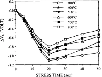
STRESS TIME (sec)
Fig. 7. Flalband voltageshift(AVFB) vs. bias-temperature stress time
for Cu/Si02/Si capacitors annealed at various temperatures; the bias-temperature stress was conducted at 150°C with an applied electrical bias of MV/cm.
Cu/Si03(1000 A)/Si capacitors, the flatband voltage as a
function of BTS time with an electrical bias of 1 MV/cm is
illustrated in Fig. 6. The flatband voltage shifted toward
more negative voltage during the first 20 s and slightly
shifted back afterward. Since the BTS was applied with
positive voltage on the gate electrode, the negative VFB shift
implies that a large amount of Cu ions drifted quickly
toward the SiO,/Si interface, even at a low temperature of 150°C. To ensure that the samples were not contaminated
by other mobile ions such as Na ions, control samples
were also fabricated following the same processing
sequence of the Cu/SiO,/Si capacitors except that Al gate instead of Cu metallization was applied for the fabrication of MOS capacitors. For the control samples, no obvious flatband voltage shift with respect to BTS was observed, indicating that the sample process was free from Na ion contamination. Figure 7 shows the flatband voltage shift as a function of bias-temperature stress time, derived from the data shown in Fig. 6, for the samples annealed at various temperatures. It reveals an interesting feature thatthe VFfl of higher temperature annealed samples are smaller than those of lower temperature annealed ones.
Since the samples annealed at a higher temperature
resulted in a larger amount of Cu ions in the Si02 layer, as indicated by a larger shift of VFB shown in Fig. 4, they should also have a larger flatband voltage shift when theseCu ions drifted toward the SiO,/Si interface. From the
contrary results shown in Fig. 7, together with the
obser-780AS102
ZRTA
4 5
6 7
8 9 10 11Ebd(MV/cm)
Fig. 8. Statistical failure cumulation of E for the thermal oxide
Cu/Si02 (780 A)/Si MOS capacitor after 30s RTA at various temper-atures in N2 ambient.
Ebd (MV/cm)
Fig. 9. Statistical failure cumulation of E for the Cu/TiN
(1200 A)/Si02 (786 A)/Si structure after 30s RTA at various temper-atures in N2 ambient.
vationthat zXV started to decrease after 20 s BTS, it is reasonable to presume that a certain amount of Cu ions near the SiO,/Si interface drifted into the Si substrate
under prolonged BTS, especially for the samples annealed at higher temperatures.
Dielectric degradation of the Si02 layer in the
metal/SiO,/Si structure after high temperature treatment mostly results from the chemical reaction between metal and Si02 as well as metal dissolution in the Si02 layer.'-'3 For example, Ti was reported to degrade the Si02 by the formation of Ti-rich suicide at the Si02/Si interface at atemperature as low as 400°C. In the Pt/SiO,/Si system,
dielectric degradation caused by Pt dissolution was report-ed.9 In Cu-related dielectric degradation, it was reported that the Si02 layer thermally grown from the Cu implant-ed Si substrate degradimplant-ed due to the Cu precipitates at the SiO,/Si interface.'4 It was also reported that contamination by scraping a piece of Cu wire over the back side of the Si
wafer caused degradation to the thermally grown Si02
layer because of the formation of Cu-rich precipitates at
Fig. 10. Stotisticcil failure cumulation of E for the Cu/TiW
(1200 A)/5i02 (786 A)/Si structure after 30 s RTA at various temper-atures in N2 ambient.
R
-0
>
>
4) 4) > E0
0 10 20 30 40 50 5 6 7 89
10 11 S I) > '4 25 20 15 10 5 4.3 I-4) E0
—0--25 20 15 10 5 0 300°C 350°C 400°C 500°C 600°C 700°C 800°C 900°C U 5 6 7 89
10 11 E bct (MV/cm)
the Si02/Si interface.15 Both studies concluded that the
dielectric degradation resulted from the Si02 thickness
reduction caused by the Cu silicide formation at the
Si02/Si interface. Since Cu diffuses quickly in Si and forms
Cu-Si compounds at a low temperature of 200°C, the Cu,
whether implanted in Si or scraped over the back side of an
Si wafer, can easily diffuse and accumulate at the Si02/Si interface to form Cu precipitates during a subsequent
ther-mal process. It was also observed that Cu4Si phase
appeared in the C/Cu/Si02/Si structure after annealing at700°C for 72 h in an N2 +H2ambient.16 Recent study shows
that Cu in the Cu/Si02/Si structure can diffuse into the
Si02 layer to a concentration of 1017 cm3 after thermal annealing at 300°C for 30 mm without bias.6 For the
Cu/Si02/Si structure studied in this work, we observe no
chemical reaction between Cu and Si02 up to 900°C of 30 s ETA. However the mobile ion and D11 measurements
indi-cated that a large number of Cu ions diffused into the Si02 layer. Furthermore, Cu ions drift very quickly in the Si07 layer and into the Si substrate under the bias-temperature
stress at a temperature of 150°C. In addition to the presence
of mobile Cu ions in the Si02 layer and the increase of interface trap density, dielectric properties of the Si02
layer were severely degraded when the MOS structure was ETA annealed at 300°. The role of Cu in the Cu/Si07/Si MOS structure is now clear. Copper is metallurgically sta-ble with the enclosed Si02 dielectric, but it is an uncon-trollable diffusion species penetrating almost freely in the
Si02/Si system; the electric bias further accelerates the
speed of penetration. Thus, the Cu metallization system must incorporate with an appropriate diffusion barrier, so that Cu could be possibly useful in ULSI applications.
Diffusion barrier effects—We investigate the
Cu/(barri-er)/5i02/Si system with respect to the diffusion barrier
effect of TiN and TiW layers, both of which are 1200 A
thick in this study. Without using the barrier layer, the
breakdown field (EM) statistic distribution of the Cu/Si02
(780 A)/Si samples annealed with 30 s ETA at various
tem-peratures is illustrated in Fig. 8. It can be seen that dielec-tric degradation started to occur following the 30 s ETA at 350°C and became worse with the increase of annealing temperature. With the barrier layer, the Ebd statistic distri-butions of the Cu/TiN/Si02/Si and Cu/TiW/Si02/Si
sam-ples annealed at various temperatures are illustrated in
Fig. 9 and 10, respectively. For the Cu/TiNfSiO2/Si
sam-ples, obvious dielectric degradation was observed after
ETA annealing at temperatures above 600°C. The failure
distribution also indicates that the degradation which
occurred was fairly nonuniform. For the Cu/TiW/Si02/Si samples, annealing at temperatures below 600°C did not cause obvious dielectric degradation, but some of the 25
randomly chosen samples started to show degradation
after annealing at 7 00°C. By comparing the data shown in Fig. 9 and 10, we clearly observe that TiW serves as a bet-ter diffusion barrier than does TiN. This is consistent with the results from the studies done on the TiN and TiW
dif-fusion barriers employed in the Cu/(barrier)/CoSi2/pn junction diodes.17'18
Conclusion
Copperwas found to be metallurgically stable with the dielectric Si02. However, Cu from the Cu/Si02/Si structure
degrades the dielectric properties of Si02 at a temperature
of 3 00°C; the higher the temperature, the more positive Cu
ions migrate into the Si02 layer, thus leading to worse
degradation of the MOS structure. In addition, Cu induces a large midgap interface trap density at the Si02/Si inter-face following ETA annealing. Under bias-temperature
stress, Cu ions drift very fast in the Si02 layer and may drift across the 5i02/Si interface and enter into Si
sub-strate. Both TiN and TiW were shown to be effective
diffu-sion barriers in the Cu/(barrier)/Si02/Si MOS structure. Without the diffusion barrier, the SiO, dielectric started to degrade following ETA at 300°C. With the use of 1200 A
TiN and TiW barrier layers, respectively, the dielectric
strength of the MOS structures remained stable up to 500
and 600°C.
Acknowledgments
The authors wish to thank the National Nano Device Laboratory and the Semiconductor Research Center of
National Chiao-Tung University for providing excellent processing environments. This work was supported by the National Science Council, EOC, under Contract No.
NSC-84-22 15-E-009-045.
Manuscript submitted July 12, 1995; revised manuscript
received Nov. 27, 1995.
National Chiao-Tung University assisted in meeting the publication costs of this article.
REFERENCES
1. A. Cros, M. 0. Aboelfotoh, and K. N. Th, J. Appl. Phys.,
67, 3328 (1990).
2. P. Padiyath, J. Seth, S. V. Babu, and L. J. Matienzo,
ibid., 73, 2326 (1993).
3. L. Stolt and F M. D'heurle, Thin Solid Films, 189, 269
(1990).
4. J. Echigoya, H. Enoki, T. Satoh, T Waki, M. Otsuki, and T. Shibata, Appl. Surf Sci., 56-58, 463 (1992).
5. 5. D. Brotherton, J. E. Ayres, A. Gill, H. W. van
Kesteren, and F. J. A. M. Greidanus, J. Appl. Phys.,62, 1826 (1987).
6. Y. Shacham-Diamand, A. Dedhia, D. Hoffstetter, and
W G. Oldham, This Journal, 140, 2427 (1993).
7. E. H. Nicollian and J. E. Brews, MOS Physics and Technology, Wiley, New York (1982).
8. C. Y Ting, M. Wittmer, S. S. Iyer and S. B. Brodsky,
This Journal, 131, 2934 (1984).
9. B. Y. Tsui and M. C. Chen, Solid State Electron., 36,
583 (1993).
10. E. Lamber N. Jaeger, and G. Schulz-Ekloff, Surf. Sci.,
227, 268 (1990).
11. J. C. Barbour, A. E. M. J. Fisher and J. F van der Veen, J. Appl. Phys., 62, 2582 (1987).
12. B. S. Chen and M. C. Chen, This Journal, 141, 1931
(1994).
13. T. H. Distefano, J. Appl. Phys., 44, 527 (1973).
14. K. Honda, A. Ohsawa, and N. Toyokura, Appl. Phys.
Lett., 45, 270 (1984).
15. H. Wendt, H. Cerva, V Lehmann, and W Pamler, J.
Appl. Phys., 65, 2402 (1989). 16. C. A. Chang, ibid., 66, 1163 (1989).
17. J. C. Chiou and M. C. Chen, This Journal, 141, 2804
(1994).