High-Reliability Ta
2O
5Metal–Insulator–Metal Capacitors with
Cu-Based Electrodes
Kou-Chiang Tsai,aWen-Fa Wu,b,
*
,zChuen-Guang Chao,aand Cheng-Ping Kuanb a
Department of Materials Science and Engineering, National Chiao Tung University, Hsinchu, Taiwan
b
National Nano Device Laboratories, Hsinchu, Taiwan
The properties of tantalum oxide共Ta2O5兲 metal–insulator–metal 共MIM兲 capacitors with Al/Ta/Cu/Ta bottom electrodes were investigated. An ultrathin Al film successfully suppresses oxygen diffusion in the Ta2O5 MIM capacitor with the Cu-based electrode. The electrical characteristics and reliability of Ta2O5MIM capacitors are improved by addition of ultrathin Al films. Ta2O5 MIM capacitors have low leakage current density共1 nA/cm2 at 1 MV/cm兲 and high breakdown field 共5.2 MV/cm at 10−6A/cm2兲. The decrease in leakage current is attributed to the formation of a dense and uniform Al
2O3 layer, which has self-protection property and stops further oxygen diffusion into the tantalum contact. The dominant conduction mechanism of leakage current is the Poole–Frenkel effect at electric fields above 1.5 MV/cm.
© 2006 The Electrochemical Society. 关DOI: 10.1149/1.2185283兴 All rights reserved.
Manuscript submitted March 10, 2005; revised manuscript received January 16, 2006. Available electronically March 27, 2006.
Metal–insulator–metal共MIM兲 capacitors are used as radio fre-quency共rf兲 capacitors in high-frequency circuits and analog capaci-tors in mixed-signal integrated circuit共IC兲 applications due to their high conductive electrodes and low parasitic capacitance.1-3As the circuit density increases, materials with a dielectric constant 共兲 much higher than SiO2共⬃3.9兲 are desired.4Among various high- dielectric candidates, tantalum pentoxide共Ta2O5兲 has been studied as a promising material for a gate dielectric of metal-oxide semicon-ductor field effect transistors because of its high dielectric constant and excellent thermal and chemical stability.5,6
Current semiconductor technology demands the use of low-resistivity metals as electrode materials for ultralarge-scale inte-grated共ULSI兲 conduction lines and contact structures. In order to minimize the cost of ownership aspect in the electrode processes, several metallization technologies have been proposed in IC appli-cations. Platinum共Pt兲 and ruthenium 共Ru兲 have been used as the electrodes of capacitors with high-dielectric materials.7,8Pt and Ru, however, have limitations for application due to their high resistivity 共Pt: ⬃ 10.6 ⍀ cm, Ru: ⬃ 7.7 ⍀ cm兲, cost, and leakage current.9 Cu-based metallization technology could be incorporated into de-vices owing to ease of processing and reduction in production cost of silicon rf capacitors and mixed-signal ICs. In addition, Cu has low resistivity共1.67 ⍀ cm兲 and high electro- and stress-migration resistance. However, Cu oxidizes during the initial stage of Ta2O5 reactive sputtering, and hillocks or particles are observed after an-nealing in oxygen ambient.10,11Significant efforts have been made to identify an appropriate diffusion barrier layer for Cu-based elec-trodes. Among these diffusion barrier materials, tantalum 共Ta兲 is selected for Cu-based electrodes because it not only has low resis-tivity but also is thermodynamically stable with Cu.12,13
Unfortunately, the grain boundaries of a sputtered Ta layer gen-erally provide paths for oxygen and copper diffusion when forma-tion of Ta2O5dielectrics requires processing under high temperature and oxygen ambient. Protection against oxidation and copper pen-etration is essential when growing Ta2O5 dielectric films on Cu-based electrodes. A capacitor structure using an ultrathin Al layer inserted between Ta2O5dielectric and Ta diffusion barrier is pro-posed in this study. The improved characteristics of Ta2O5 MIM capacitors are investigated.
Experimental
Thermally grown SiO2films were formed on p-type Si共100兲 sub-strates for isolation. Three types of Cu-based bottom electrode layers were deposited by sputtering, 共a兲 Cu 共300 nm兲/Ta
共50 nm兲, 共b兲 Ta 共50 nm兲/Cu 共300 nm兲/Ta 共50 nm兲, and 共c兲 Al共20 nm兲/Ta 共30 nm兲/Cu 共300 nm兲/Ta 共50 nm兲. The Ta film was deposited first and the Al film was the top layer for Al/Ta/Cu/Ta electrode layers. The Al/Ta/Cu/Ta electrode multilayers were formed by sequential sputtering of metal targets without breaking vacuum. Ta2O5 films of 40-nm thickness were deposited on Cu-based electrodes by reactive sputtering using a Ta target. During Ta2O5deposition, Ar and O2mixture gases were introduced into the chamber to produce a total pressure of 3.5 mTorr. After Ta2O5films were deposited, some wafers were postannealed at 500–600ⴰC in oxygen ambient for 30 min. Then 50-nm Ta and 100-nm Cu films were deposited sequentially as top electrodes. Table I lists the MIM structures with multilayered bottom electrodes in the study.
The film thickness and refractive index were measured by field emission scanning electron microscopy共FESEM兲 and spectroreflec-tometry, respectively. The samples were investigated by cross-sectional transmission electron microscopy共XTEM兲 using a field emission microscope共JEOL JEM-2010F兲 and an acceleration volt-age of 200 kV. The samples were prepared by mechanical grinding and polishing followed by ion milling under an acceleration voltage of 3–5 kV in a Gatan Duomill. Chemical reaction and oxygen pen-etration profile were characterized by secondary ion mass spectrom-etry共SIMS兲 and X-ray photoelectron spectrometry 共XPS兲. Current-voltage 共I-V兲 characteristics were used to investigate the leakage current and breakdown field. The breakdown field共Ebd兲 was defined as the electrical field when the current density through the dielectric exceeds 10−6A/cm2. To evaluate the reliability of the Ta
2O5film, time-dependent dielectric breakdown共TDDB兲 measurements using constant voltage stress were performed. Capacitors with an area of 3.14⫻ 10−4cm2were employed.
Results and Discussion
Figure 1 illustrates SEM micrographs of the Ta2O5/Ta/Cu/Ta and Ta2O5/Al/Ta/Cu/Ta samples after annealing at 600ⴰC in oxygen for 30 min. As displayed in Fig. 1a, the Ta2O5/Ta/Cu/Ta sample becomes rugged and forms particles and hillocks on the surface. Normally, oxygen easily penetrates the Ta layer via active diffusion paths and oxidizes the underlying layer. As shown in Fig. 1b, how-ever, no hillocks are observed on the Ta2O5/Al/Ta/Cu/Ta sample surface. This indicates that Al/Ta barrier is impermeable to oxygen diffusion and protects the Cu layer underneath from oxidation.
Figure 2a illustrates the SIMS depth profiles of the O elements in the Ta2O5/Ta/Cu/Ta sample following annealing at 500 and 600ⴰC in oxygen ambient. The annealing was performed after the Ta2O5 film was deposited. Oxygen diffusion is found after annealing. The oxygen contents in Ta and Cu films increase with increasing anneal-ing temperature. Oxygen atoms diffuse along the grain boundaries of the Ta crystal and react with the Ta layer during annealing. The *Electrochemical Society Active Member.
z
HRTEM image in Fig. 2b clearly shows that an interlayer of 4–5 nm thickness is formed between Cu and Ta layers after annealing at 600ⴰC in oxygen. Figure 3a displays the SIMS depth profiles of the O elements in the Ta2O5/Al/Ta/Cu/Ta sample after annealing at 500 and 600ⴰC. Almost no indication exists that oxygen atoms diffuse into the Ta and Cu layer. The SIMS observation shown is consistent with the HRTEM micrograph of Ta2O5/Al/Ta/Cu/Ta structures 共Fig. 3b兲 after annealing at 600ⴰC in oxygen. No oxygen defection or reaction is observed between the Ta and Cu layers in the
Ta2O5/Al/Ta/Cu/Ta samples. Significant improvement in thermal stability is obtained, compared with the samples without thin Al film, apparently due to the barrier effectiveness of Al/Ta layers. However, the effective dielectric constant is about 18 instead of the value of 25 for pure Ta2O5. Figure 4 shows the TEM micrograph of the Cu/Ta/Ta2O5/Al/Ta/Cu device after thermal annealing at 600ⴰC and reveals that the ultrathin film with an amorphous structure is formed between Ta2O5and Al layers.
To identify this amorphous layer, the O 1s XPS spectra of Ta2O5 films deposited on Ta/Cu/Ta and Al/Ta/Cu/Ta electrodes were ana-lyzed and are depicted in Fig. 5. Ta2O5films were sputtered onto the electrodes for 5 min to form a layer of Ta2O5 of thickness 艋10-nm and then both samples were ion-etched in order to expose the interfaces of the Ta2O5–Ta and Ta2O5–Al. The O 1s spectra pre-sented in Fig. 5a show that the oxygen photoelectrons are in the Ta–O state. The standard O 1s peak position is located at⬃531 eV. The O 1s spectra presented in Fig. 5b show that the oxygen photo-electrons are in the Ta–O and Al–O states, indicating formation of an Al2O3layer.14In fact, formation of a dense monolayer of Al2O3 layer results in self-protection to oxidation and stops further oxygen diffusion. The layer behaves as an effective diffusion barrier to pro-tect the underlying Cu and Ta layers.15,16The formation of Al2O3is thermodynamically favorable compared to Cu oxide due to the large difference in oxide formation energy between Al共−226 kcal/g mol Table I. MIM capacitors with various multilayered bottom
electrodes used in the study.
Sample
Top electrode
共nm兲 Insulator共nm兲 Bottom electrode共nm兲 共a兲 Cu共100兲/Ta 共50兲 Ta2O5共40兲 Cu共300兲/Ta 共50兲 共b兲 Cu共100兲/Ta 共50兲 Ta2O5共40兲 Ta共50兲/Cu 共300兲/Ta 共50兲 共c兲 Cu共100兲/Ta 共50兲 Ta2O5共40兲 Al 共20兲/Ta 共30兲/Cu 共300兲/
Ta共50兲
Figure 1. SEM images of the Ta2O5 films on 共a兲 Ta/Cu/Ta and 共b兲 Al/Ta/Cu/Ta bottom electrodes after annealing at 600ⴰC for 30 min in oxygen ambient.
Figure 2. 共a兲 SIMS depth profiles of O elements in the Ta2O5/Ta/Cu/Ta samples after furnace annealing at 500 and 600ⴰC for 30 min in oxygen ambient.共b兲 HRTEM image of the interlayer between Ta and Cu layers in the Ta2O5/Ta/Cu/Ta sample.
G493
O2兲 and Cu 共−53 kcal/g mol O2兲. Therefore, the Al2O3layer will behave as an effective diffusion barrier to protect the underlying Cu and Ta layers.
Figure 6 displays leakage current densities of Ta2O5films depos-ited on Al/Ta/Cu/Ta bottom electrodes after annealing at various temperatures in O2ambient. The thickness of the dielectric layer is the total thickness of the Ta2O5and Al2O3films. The leakage cur-rent density of the as-deposited Ta2O5 film is⬃100 nA/cm2 and decreases to⬃1 nA/cm2at 1 MV/cm after annealing at 600ⴰC due to elimination of oxygen vacancies and bond defects. Atanassova et al. have reported that oxygen annealing may affect the concentration of the oxygen vacancies and nonperfect bonds in the initial layers and consequently leads to leakage current reduction.17Several post-deposition treatments were investigated and successfully applied to reduce the oxygen vacancies and improve the electrical properties of Ta2O5 thin film.6 Electrical properties of Ta2O5 MIM capacitors with various bottom electrodes, including Cu/Ta, Ta/Cu/Ta, and Al/Ta/Cu/Ta, were further compared and investigated. Figure 7 dis-plays the leakage current densities as a function of electrical field up to 6 MV/cm following annealing at 600ⴰC for 30 min. The leakage current densities are ⬃250 and 1.2–1.5 nA/cm2 at 1 MV/cm for Cu/Ta and Ta/Cu/Ta bottom electrodes. The lowest leakage current density of 1 nA/cm2is measured for the Al/Ta/Cu/Ta bottom elec-Figure 3. 共a兲 SIMS depth profiles of O elements in Ta2O5/Al/Ta/Cu
samples after furnace annealing at 500 and 600ⴰC for 30 min in oxygen ambient.共b兲 HRTEM image of the region between Ta and Cu layers in the Ta2O5/Al/Ta/Cu/Ta sample.
Figure 4. TEM image of the Cu/Ta/Ta2O5/Al/Ta/Cu/Ta MIM capacitor. The annealing was conducted at 600ⴰC for 30 min in oxygen ambient after Ta2O5film was deposited.
Figure 5. O 1s XPS spectra obtained from 共a兲 Ta2O5–Ta interface for the Ta2O5/Ta/Cu/Ta sample and 共b兲 Ta2O5–Al interface for the Ta2O5/Al/Ta/Cu/Ta sample.
trode. Also, the leakage current densities of Ta2O5MIM capacitors with Al/Ta/Cu/Ta bottom electrodes are much lower than those re-ported by Ezhivalavan and Tseng.10,18The breakdown field共Ebd兲 for the Al/Ta/Cu/Ta bottom electrode is approximately 5.2 MV/cm共at 10−6A/cm2兲 and higher than those for the Cu/Ta and Ta/Cu/Ta bottom electrodes of around 1.4 and 3.7 MV/cm.
Leakage current is a key parameter for ULSI circuit applications. The leakage current in the Ta2O5 MIM capacitor may be due to several mechanisms, including Schottky emission, Poole–Frenkel effect, electronic-hopping conduction, and tunneling.6,17,19,20 The leakage current density vs electric field共J-E兲 characteristics of the MIM capacitor using bottom and top electrodes of different work functions are highly asymmetric with the voltage polarity for the Schottky emission and symmetric for the Poole–Frenkel emission.21 In this study, symmetric J-E characteristics were observed for Ta2O5 MIM capacitors with Al/Ta/Cu/Ta bottom electrodes and Ta/Cu top electrodes. This behavior indicates that Poole–Frenkel emission is the possible dominant conduction mechanism for leakage currents. The Poole–Frenkel effect predicts a field-dependent behavior of the form J = CE exp
冉
−q0 kT冊
exp冉
PF kTE 1/2冊
关1兴where J denotes current density, T denotes the absolute temperature,
q is the electronic charge,0is the barrier height, k represents the Boltzmann constant, E represents electric field, C is a constant, and  is defined by PF=
冉
q 3 0冊
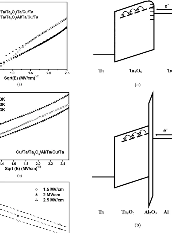
1/2 关2兴 where0is the permittivity of free space and denotes the high-frequency dielectric constant. Poole–Frenkel conduction is due to field-enhanced thermal excitation of trapped electrons in the insula-tor into the conduction band. Figure 8a shows the logarithmic cur-rent density divided by the electric field as a function of the square root of the electric field关ln共J/E兲 vs E1/2兴. A good linearity is ob-served for the field E⬎ 1.5 MV/cm for the plots. Furthermore, the dielectric constant deduced from the slope of the linear region of the Poole–Frenkel emission graph yields an ⑀ value of 9.21, almost equal to that measured. The results indicate that the conduction mechanism is dominated by Poole–Frenkel effect for the field E ⬎ 1.5 MV/cm. In the case of the Al/Ta/Cu/Ta bottom electrode, the temperature dependence of J-E characteristics of the Ta2O5 capaci-tors was further studied. The leakage current increases exponentially with the temperature, as shown in Fig. 8b and c. These results reveal that it is affected by trap charge density, and the behavior shown in these plots indicates the Poole–Frenkel mechanism.Figure 9a and b illustrates conduction mechanisms of Ta2O5 MIM capacitors with Ta/Cu/Ta and Al/Ta/Cu/Ta bottom elec-trodes. Some activated oxygen in the Ta2O5film could diffuse into the Ta/Cu/Ta bottom electrode and react with the Ta layer during annealing. The oxygen vacancy acts as an electron trap with certain trap levels in the energy band diagram. The traps act as stepping sites for electrons and facilitate their transport through the oxide. Moreover, the barrier height becomes low when the oxygen vacan-cies accumulate at the interface of the Ta2O5–metal electrode.22 Ta/Cu/Ta bottom electrodes could result in more oxygen vacancies at the Ta2O5–Ta interface compared to Al/Ta/Cu/Ta bottom elec-trodes. When the top electrode is positively biased, electrons are relatively easily injected from the Ta/Cu/Ta bottom electrode into the tantalum oxide layer and further conductivity is governed by Poole–Frenkel effect共Fig. 9a兲. An interfacial Al2O3layer is formed at the Ta2O5–Al interface for the Al/Ta/Cu/Tabottom electrode. The formation of this layer can lead to modification of the conduction mechanism due to the difference in the bandgaps of Ta2O5 and Al2O3. Ta2O5 and Al2O3 have bandgaps of 4.4 and 8.8 eV, respectively.23It is found that the dominant conduction mechanism is also Poole–Frenkel effect for the Al/Ta/Cu/Ta bottom electrode from analyses of J-E characteristics. However, the interfacial Al2O3 layer will result in self-protection to oxidation and stop further oxy-gen diffusion. Reduction of oxyoxy-gen vacancies leads to decreasing trap site, and leakage currents of Ta2O5 MIM capacitors with Al/Ta/Cu/Ta bottom electrodes could be reduced.
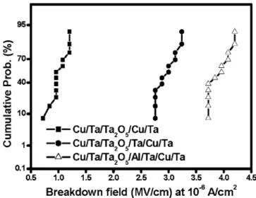
Nowadays, the TDDB is an important reliability indicator of the MIM capacitor. Figure 10 illustrates cumulative probabilities of breakdown fields for Ta2O5 MIM capacitors with various bottom electrodes. Breakdown is defined as occurring when the leakage current density increases to 10−6A/cm2. Obviously, the Cu/Ta/Ta2O5/Al/Ta/Cu/Ta MIM capacitors exhibit better break-down behaviors than Cu/Ta/Ta2O5/Ta/Cu/Ta and Cu/Ta/Ta2O5/Cu/Ta MIM capacitors. Figure 11 shows the TDDB lifetime as a function of electric field for Ta2O5 MIM capacitors with various bottom electrodes. The Ta2O5 MIM capacitors with Al/Ta/Cu/Ta bottom electrodes have a longer lifetime than the oth-ers. The extrapolated long-term lifetime indicates that the Ta2O5 MIM capacitors with the Al/Ta/Cu/Ta bottom electrodes can sur-vive 10 years at a stress field of 1.2 MV/cm. Moreover, the plotted points follow straight lines and random failure modes are not ob-Figure 6. J-E characteristics of the Cu/Ta/Ta2O5/Al/Ta/Cu/Ta MIM
capacitors after annealing at various temperatures in oxygen ambient for 30 min.
Figure 7. J-E characteristics of the Ta2O5 MIM capacitors with various bottom electrodes after annealing at 600ⴰC in oxygen ambient for 30 min.
G495
served, indicating the Ta2O5MIM capacitors with the Cu-based bot-tom electrodes are of high quality and good uniformity.
Conclusion
Multilayered Al/Ta/Cu/Ta electrodes enhance the properties of the Ta2O5 MIM capacitors with Cu-based electrodes. This work found that the capacitors demonstrated a significant improving ca-pability against oxygen diffusion after inserting an Al film. This improvement is attributed to a dense Al2O3film formed on the sur-face of the Al/Ta/Cu/Ta bottom electrode after thermal annealing in oxygen ambient. Ultralow leakage current density 共1 nA/cm2 at 1 MV/cm兲 and high breakdown field 共5.2 MV/cm at 10−6A/cm2兲 are obtained for Ta2O5 MIM capacitors with Al/Ta/Cu/Ta elec-trodes because of reducing oxygen vacancy in tantalum oxide films. Figure 8.共a兲 ln共J/E兲 vs E1/2plots for the Ta
2O5MIM capacitors.共b兲 ln共J/E兲 vs E1/2 plots for the Ta
2O5 MIM capacitors with Al/Ta/Cu/Ta bottom electrodes at various measurement temperatures.共c兲 ln共J/E兲 vs 1000/T plots for the Ta2O5MIM capacitors with Al/Ta/Cu/Ta bottom electrodes.
Figure 9. Schematic illustration of conduction mechanisms in Ta2O5MIM capacitors with共a兲 Ta/Cu/Ta and 共b兲 Al/Ta/Cu/Ta bottom electrodes biased at a positive voltage.
Ta2O5MIM capacitors with Al/Ta/Cu/Ta electrodes also show less charge-trapping and better TDDB properties. Al/Ta/Cu/Ta
elec-trodes enable the integration of Cu elecelec-trodes with high-dielectric-constant tantalum oxide thin films for high-frequency devices at interconnect levels.
Acknowledgments
The work was financially supported by the National Science Council of the Republic of China under contract no. NSC 94-2215-E-492-009 and supported, in part, by the Ministry of Economic Af-fairs of the Republic of China under contract no. 93-EC-17-A-08-S1-0003. Technical support from the National Nano Device Laboratories is gratefully acknowledged.
National Nano Device Laboratories assisted in meeting the publication costs of this article.
References
1. J. A. Babcock, S. G. Balster, A. Pinto, C. Dirnecker, P. Steinmann, R. Jumpertz, and B. El-Kareh, IEEE Electron Device Lett., 22, 230共2001兲.
2. M. Armacost, A. Augustin, P. Felsner, Y. Feng, G. Friese, J. Heidenreich, G. Hueckel, O. Prigge, and K. Stein, Tech. Dig. - Int. Electron Devices Meet., 2000, 157.
3. A. Kar-Roy, C. Hu, M. Racanelli, C. A. Compton, P. Kempf, G. Jolly, P. N. Sherman, J. Zheng, Z. Zhang, and A. Yin, in Proceedings of the IITC, p. 245 共1999兲.
4. R. B. van Dover, R. M. Fleming, R. M. Schneemeyer, G. B. Alers, and D. J. Werder, Tech. Dig. - Int. Electron Devices Meet., 1998, 823.
5. W. D. Kim, J. H. Joo, Y. K. Jeong, S. J. Won, S. Y. Park, S. C. Lee, C. Y. Yoo, S. T. Kim, and J. T. Moon, Tech. Dig. - Int. Electron Devices Meet., 2001, 263. 6. C. Chaneliere, J. L. Autran, R. A. B. Devine, and B. Balland, Mater. Sci. Eng., R,
R22, 269共1998兲.
7. S. Ezhilvalavan and T. Y. Tseng, J. Appl. Phys., 83, 4797共1998兲.
8. J. W. Lee, H. S. Song, K. M. Kim, J. M. Lee, and J. S. Roh, J. Electrochem. Soc., 149, F56共2002兲.
9. J. H. Joo, J. M. Seon, Y. C. Jeon, K. Y. Oh, J. S. Roh, and J. J. Kim, Appl. Phys.
Lett., 70, 3053共1997兲.
10. S. Ezhilvalavan and T. Y. Tseng, Thin Solid Films, 360, 268共2000兲.
11. W. Fan, S. Saha, J. A. Carlisle, O. Auciello, R. P. H. Chang, and R. Ramesh, Appl.
Phys. Lett., 82, 1452共2003兲.
12. W. L. Yang, W. F. Wu, D. G. Liu, C. C. Wu, and K. L. Ou, Solid-State Electron., 45, 149共2001兲.
13. W. F. Wu, K. L. Ou, C. P. Chou, and C. C. Wu, J. Electrochem. Soc., 150, G83 共2003兲.
14. J. F. Moulder, W. F. Stickle, P. E. Sobol, and K. D. Bomben, Handbook of X-ray
Photoelectron Spectroscopy, p. 44 Physical Electronics, Eden Prairie, MN共1995兲. 15. W. A. Lanford, P. J. Ding, W. Wang, S. Hymes, and S. P. Muraka, Thin Solid Films,
262, 234共1995兲.
16. W. A. Lanford, S. Bedell, P. Isberg, B. Hjovarsson, S. K. Lakshmanan, and W. N. Gill, J. Appl. Phys., 85, 1487共1999兲.
17. E. Atanassova, N. Novkovski, A. Paskaleva, and M. P. Gjorgjevich, Solid-State
Electron., 46, 1887共2002兲.
18. S. Ezhilvalavan and T. Y. Tseng, in Proceedings of the Electronic Components and
Technology Conference, p. 1042共1999兲.
19. S. M. Sze, Physics of Semiconductor Device, p. 478 Wiley, New York共1981兲. 20. C. Chaneliere, J. L. Autran, and R. A. B. Devine, J. Appl. Phys., 86, 480共1999兲. 21. C. S. Chang, T. P. Liu, and T. B. Wu, J. Appl. Phys., 88, 7242共2000兲. 22. J. H. Joo, Y. C. Jeon, J. M. Seon, K. Y. Oh, J. S. Roh, and J. J. Kim, Jpn. J. Appl.
Phys., Part 1, 36, 4382共1997兲.
23. J. Robertson, Appl. Surf. Sci., 190, 2共2002兲. Figure 10. Cumulative probabilities of breakdown fields for Ta2O5 MIM
capacitors with various bottom electrodes.
Figure 11. TDDB lifetime as a function of electric field for Ta2O5 MIM capacitors with various bottom electrodes.
G497