M.
C.
Lee,C.
R.
Huang,Y.
S.
Chang, andY.
F.
ChaoDepartment ofElectrophysics and Institute ofElectro Op-tical Engineering, National Chiao Tung University, Hsin Chu, Taiwan 30049,TheRepublic ofChina
(Received 6 April 1989;revised manuscript received 21 July 1989)
Amorphous silicon films after picosecond laser excitation have been investigated by Raman mi-croprobe analysis. The recrystallized Raman peak intensity can be more than four times that of crystalline Si. By carefully examining the annealed microstructure, the enhancement isinterpreted asa double-resonance effectdue tomicrocrystals.
I.
INTRODUCTIONThe laser-induced phase transition in amorphous
sil-icon (a-Si) has been extensively studied in recent years for
fundamental interests and potential applications.
'
Us-ing laser annealing techniques on a-Si thin films, weob-served that the Raman intensity
of
the recrystallized peak can be higher than four times thatof
crystalline silicon(c-Si). Bytaking the Raman intensity ratio
of
annealed Sito c-Si
(I,
„„„„d/I,
s;) and tuning the probe wavelength from the visible to the ultraviolet (uv), the Raman enhancement is revealed. This enhancement in the visi-ble (blue-green) region does not appear to be due to the resonance Raman scatteringof
c-Sinear the Eo andE,
critical points. After examining the scanning-electron microscopy (SEM) pictures
of
picosecond laser excited aSi films, we found that the annealed microstructure is within the range
of
Mie scattering resonance. However,if
wejust consider the Mie absorption cross section, ' thecalculated enhancement is not large enough. Because the Raman scattering involves absorption
of
incident light and scatteringof
Stokes and anti-Stokes photons, when both the incident and the scattered wavelengths are closeto the size
of
the annealed microcrystals, a double reso-nance could occur and give rise to the enhancement. Such an interpretation is made since the productof
the Mie absorption and scattering cross sections indeed fit our measurements will except in the long-wavelengthre-gion which is due to significant interference e6'ects.
II.
EXPERIMENTThe details
of
the film preparation were described inRef.
3.
The film thicknesses are inferred from thespec-trophotometric measurements to be
0.
8,1.
2, and1.
8pm, for the 20-,30-,and 45-min deposition time, respectively.The experimental setup for pulsed-laser annealing and Raman measurements is essentially the same as that in
Ref.
8,except a dye laser (PRA LN-107 at 580nm)of
600ps was employed. After exciting the a-Sifilms with vari-ous Auences from
0.
1to1.
4J/cm,
the microstructureof
them was examined under microscope. The Raman in-tensity was measured by microprobe
(10
pm at1/e
)(Ref.8)at
=2
mW which also serves as a monitor for thelocal structure variation. All major laser lines from
ar-gon, He-Ne to He-Cd lasers, were employed. The
scat-tered signals were imaged onto a double monochromator
(Jobin Yvon U-1000). A multichannel detector
(Prince-ton Instruments
(IRY-1024G)
was used to increase the signal-to-noise ratio by detecting a wide spectral rangefor long exposure.
For
the enhancement analyses, we take the Raman intensity ratioof
annealed Si to c-Si ateach probe wavelength instead
of
the intensity itself. Bydoing so, not only the wavelength dependence
of
theRa-man susceptibility and the detection system eKciency can be removed, but the probe power Auctuation isalso elim-inated. As the result
of
this normalization, the Raman enhancement is revealed.III.
RESULTSAND DISCUSSIONIn
Fig.
1, the Raman spectrumof
c-Siexhibits a strong and sharp peak at 520 cm ' with a linewidthof
-3
cm',
while thatof
a-Si shows a very broad feature(-60
cm ') around 475 cm'.
As the ffuence on the a-Siis in-creased to0.
16J/cm,
the broad feature diminishes and a distinct peak energies at 513 cm ' with a large width. This peak gradually shifts to 518cm ' with the increas-ing fluence.It
looks similar to thatof
c-Si after0.
38J/cm . This indicates that the recrystallization volume enlarges with the excitation. However, after excitation
~ 0.
4J/cm the Raman-enhancement eAect begins toap-pear.
For
extracting the enhancementof
the recrystal-lized Raman line, the normalized intensity data obtained by diff'erent probe photon energies (they are much larger than the Raman shift) are plotted inFig.
2 to show whether it is due to the band-gap resonance about3.
4 eV. When the excitation Auence isincreased from0.
3to1.
2J/cm,
the enhancement peak only slightly shifts from2.7 to 2.6 eV (457.9 to 476.5 nm). Its profile is sharp around
0.
4J/cm,
and becomes broadened aboveit.
This enhancement is obviously not due to the band-gap reso-nance but to the annealed microstructureof
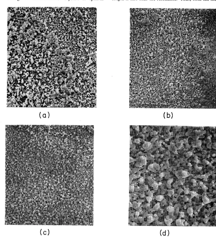
the film.The detailed structure
of
three annealed films obtained by SEM are shown in Figs. 3(a)—3(c). The fine crystals formed in thicker films(1.
2 and1.
8 pm) are in similar sizes and shapes but the thinnest film (0.8 pm) contains lotsof
larger crystals. Because the substrate is glass, there is no epitaxial growth. The ball-like particles aremixed in crystalline-amorphous structure. Thus, the
40 DOUBLE-RESONANCE-ENHANCED RAMAN SCATTERING
IN.
.
.
10421c-Si
1.
1J/c
x0.
5
0.
38J
km
0.
3
J/cm
2x1
0.
16
Jlcm
~RLl a~~
JJg~~.
~~a~~'
~pmR~Sf ~W~
~r
-
W~
.
~ 2QQa-si
320
370
I420
I4-7
0
I520
I 5 I570
620
RAMAN
SHIFT
[
cm
)FIG.
1. The Raman spectra ofc-Si and 1.2-pm a-Sifilm obtained by 488-nm probe. The recrystallized Raman intensity increaseswith the Auence that can show the annealing status directly. (X no.)indicate magnifications.
cA I 13 Q
Q3—
a 1.1 4083
0.6 Jlcrn2 v042
x 0.38 1.2 ~m filmstandard Lorenz-Mie scattering formulas for spherical particles are used
to
fit the enhancement profile. Thenormalized efficiency factors
of
absorption(Q,
b,) andscattering
(Q„,
«)cross sections, are given byoo
Q,
b,=,
g
(2p+1)[2
—
~2a„(x,
m)—
1~' 2x—
I2b„(x,
m)—
1~],
UJ QJ 1.5
2.
0
2.5
3.
0
PROBE
PHOTON ENERGY(eV)
3.
5
FIG.
2. The Raman enhancement(I,
„„„],
d/I, $;) of 1.2 pm film after diA'erent Auences vsprobe photon energy. Solid linesare the calculated Q,b,
Q„,
«and the dashed line is the calculat-ed Q,„,
for 1.1J/cm,
under asymmetric Gaussian distribution.oo
Q„„,
=
g
(2@+1)[~a„(x,
m)~+
~b„(x,
m)~2],
x
v=1(2)
where
x
=~d/A,
isthe size parameterof
particle with di-ameter d, and incident wavelength A,.
Due to the opticaldispersion
of
c-Si, the corresponding complex refractiveindices, m
=n+ik,
are used to calculate the complexelectric and magnetic multipole expansion coefficients
of
the pth order(a„and
b„)
in the Mie theory. However, the calculated enhancement for single-particle size is much narrower than what we observed.Because
of
rapid nucleation by picosecond laser pulse, the annealed microcrystals are in difFerent sizes. In addi-tion they are not isolated but connected in a porous net-work as shown 111Flg. 3(d), tile X 10klllaglllflcatlollSEM
micrograph. The real causeof
the network formation is unclear, which may be ascribable to explosive crystalliza-tion and its generated shock wave. ''"
In order to fit thesmall size deviations o.,(cr,) are introduced besides the mean particle diameter. This assumption
of
theasym-metric distribution isbased on the SEM annealed
micros-tructure and supported by the good fitting to the enhancement. Since recrystallization is more eA'ective from proper crystal size, pulsed annealing should pro-duce unequal size distribution.
Considering the submicrometer crystals as spheres
line in Fig.2)isnot as large as the measured results.
Be-cause the Raman process involves absorption
of
incident light and scatteringof
Stokes and anti-Stokes photons, a double resonance' issuspected. Since the first-orderRa-man shift
of
c-Siissmall compared with the incidentpho-ton energy
(-2%),
when the incident wavelength iscloseto the particle size for Mie resonance, the scattered wave-length is also near the resonance. Thus, both the
incom-FIG.
3. SEMmicrographs of{a)0.8-, {b)1.2-,and {c) 1.8-pm a-SiAlms excited by a 580-nm dye laser{1.
1J/cm~). There areDOUBLE-RESONANCE-ENHANCED RAMAN SCATTERING
IN.
. .
10423 4 632.8 ~ 5]4.5 nm g3 a 363.8 LU X hl2-1.2em film/
~ ~ Ul z1 X ~ a-~ I II0,
0.4 0.8 1.2 FlUENCE(J/cm )FIG.
4. The Raman enhancement vs annealing fluence. The sharp transition isresulted from a recrystallization layer which is about the probe penetration depth (300 A at 0.3 J/cm'). Above the transition, the large Auctuations are due to interfer-ence.ing and the outgoing resonances could conceivably occur, giving rise to the enhancement. Taking it in proportion tothe product
of
the Mie absorption and scattering crosssections, several annealed conditions (0.38, to
1.
1 J/cm )are analyzed by choosing (d, o
„and
o,
)from (0.09,
0.
03,
and
0.
01)
to (O.l,
O.l,
and0.01)
pm. The calculatedQ,
b,Q„,
« indeed give rise to the resonance in the wave-length domain which are in good agreement with our measurements (solid lines inFig.
2). Therefore, themi-crostructure effect is believed to be the cause
of
the enhanced Raman scattering.From
Fig.
1, the higher Raman intensity results from the stronger excitation which produces the thickerrecry-stallization layer.
For
understanding its thickness effect, we only plot the Raman enhancement versus annealing Iluence for three difFerent probes inFig.
4 (all visible probes have similar behavior). As the annealed thickness approaches the probe penetration depth, the enhance-ment sharply rises about the transition fluence(-0.
4J/cm ). Above the transition, large Auctuations are ob-served in all visible probes but no such variations ob-served in the uv
(363.
8 nm) probe. Because the uv pho-ton energy (3.4 eV) is close to the silicon direct gap, dueto the strong optical absorption, it is reasonable to esti-mate the recrystallization thickness to be 300 A at
0.
3J/cm;
If
the Raman cross sectionsof
the annealed film and c-Si are not significantly different, then the effective scattering is inversely proportional to the probe penetra-tion depth.For
the thin recrystallized layer ((
0.
4J/cm ), the scattering eKciency
of
the uv probe is larger than thatof
the visible probes. This isconsistent with the early enhancement riseof
the363.
8-nm probe and the low enhancementof
the632.
8-nm probe about0.
3J/cm.
However, for the thick recrystallized layer()
0.
4J/cm ), the large absorption at363.
8nm eventually suppresses all possible enhancement, so the normalized intensity tailsofT' to 1 (i.e., no enhancement variations). But weak ab-sorption in the long wavelength allows multipole reAection and/or scattering to occur, so that large
Auc-5.
0
I~
40
a
3.
0-UU0
UJF20
x-UJ 0 0.8 x 1.2 ~m film 1.8 after 1J/cm~
10-
gl
lX I I2.3
2.
7
3.
13.5
PROBE
PHOTON ENERGY(eV)FIG.
5. The Raman enhancement vs probe photon energy. The thinnest film has the largest enhancement. No apparent enhancement beyond 2.8eV. The large difference below 2eV is due to interference. Curves are drawn through data points.tuations are observed beyond
0.
4 J/cm for mostof
the visible probes.As shown in the SEM pictures, the annealed micro-structure is different from one film thickness to another
under the same Auence. Since the Raman enhancement is closely related to the annealed microstructure, the results
of
0.
8-,1.
2-, and1.
8-pm samples are collected inFig.
5 for comparison. Between2.
4 and 2.8 eV(514.
5to441.
6-nm blue-green region), the largest enhancement appears in the thinnest film and less prominent in the thickerones. But they all approach unity beyond
2.
8 eV, in-dependentof
the film thickness. This confirms thatstrong absorption indeed prevents any enhancing effect. However, the situation below 2 eV is complicated, which can vary from
0.
5 to more than 2 as compared with c-Sidepending on both the excitation fluence and the film thickness. An interference-enhanced Raman scattering
on a relatively transparent multilayer Ti02/SiO2 from
570 to 630 nm was observed by Craig et
al.
Becauseof
weak absorption at1.
96 eV (632.8 nm), the interference effect has to be considered in our experiment to account for the large enhancement variation. Nevertheless, forprobe wavelengths between
2.
4 and2.
8 eV, the sharp enhancement feature can we11 be explained by theDue to the annealed microstructure eA'ect, the Raman enhancement
of
a-Si films is well interpreted as a double resonance by using Mie scattering formulas between 2.4and
2.
8 eV. In long-wavelength probes, the multiple in-terference eA'ect becomes important and causes intensity variations. However, strong absorption in short wave-lengths prevents any enhancement from happening.We are grateful to Professor
Y.
C.
Lee for his valuable suggestions. %'e also appreciate Mr. S.Y.
Wu for his technical help in taking the SEM pictures. The financial support from the National Science Councilof
theRepub-lic
of
China isalso acknowledged.~Amorphous Silicon Semiconductors —Pure' and Hydrogenated,
Vol. 95 ofthe Materials Research Society Proceedings, edited
by A. Madan, M. Thompson, D. Adler, and Y.Hamakawa {MRS,Pittsburgh, PA, 1987).
2M. Bohm, Solid State Technol.,September (1988).
M. C.Lee, C.
J.
Tseng, C.R.Huang, andT.
H.Huang, Jpn.J.
Appl. Phys. 26, 193(1987).
~A. Compaan and H.
J.
Trodahl, Phys. Rev. B 29,793(1984). 5D. V.Murphy and S.R.
J.
Brueck, Opt. Lett. 8,494(1983).S.
R.
J.
Brueck, in Laser Processing and Diagnostics, Vol. 39ofSpringer Series in Chemica/ Physics, edited by D. Bauerle (Springer-Verlag, Berlin, 1984), p.446.
7R. A. Craig, G.
J.
Exarhos,%.
T.Pawlewicz, andR.
E.
Willi-ford, Appl. Opt. 26, 4193 (1987).
M. C.Lee, C.
R.
Huang, and C.C.Lin, Jpn.J.
Appl. Phys. Suppl. 26,67(1987).D.
F.
Edwards, in Handbookof
Optical Constants ofSolids,edited by
E.
D. Palik (Academic, New York, 1985), pp. 547-569.M. O.Thompson, G.
![FIG. 2. The Raman enhancement (I, „„„], d/I, $;) of 1. 2 pm film after diA'erent Auences vs probe photon energy](https://thumb-ap.123doks.com/thumbv2/9libinfo/7587110.127003/2.918.86.436.652.1023/raman-enhancement-after-erent-auences-probe-photon-energy.webp)