Effect of oxygen on characteristics of nickel oxideindium tin oxide heterojunction
diodes
Hung-Lu Chang, T. C. Lu, H. C. Kuo, and S. C. Wang
Citation: Journal of Applied Physics 100, 124503 (2006); doi: 10.1063/1.2404466
View online: http://dx.doi.org/10.1063/1.2404466
View Table of Contents: http://scitation.aip.org/content/aip/journal/jap/100/12?ver=pdfcov Published by the AIP Publishing
Articles you may be interested in
Near-ideal electrical properties of InAs/WSe2 van der Waals heterojunction diodes Appl. Phys. Lett. 102, 242101 (2013); 10.1063/1.4809815
Fabrication of zinc oxide nanorods based heterojunction devices using simple and economic chemical solution method
Appl. Phys. Lett. 93, 083124 (2008); 10.1063/1.2975829
Fabrication and photoresponse of a pn -heterojunction diode composed of transparent oxide semiconductors, p-NiO and n- ZnO
Appl. Phys. Lett. 83, 1029 (2003); 10.1063/1.1598624
Fabrication of transparent p–n heterojunction thin film diodes based entirely on oxide semiconductors Appl. Phys. Lett. 75, 2851 (1999); 10.1063/1.125171
Fabrication of n -type nickel doped B 5 C 1+ homojunction and heterojunction diodes Appl. Phys. Lett. 70, 1028 (1997); 10.1063/1.118434
Effect of oxygen on characteristics of nickel oxide/indium tin oxide
heterojunction diodes
Hung-Lu Chang, T. C. Lu,a兲H. C. Kuo, and S. C. Wang
Institute of Electro-Optical Engineering, National Chiao Tung University, Hsinchu, 30050 Taiwan, Republic of China
共Received 21 June 2006; accepted 20 October 2006; published online 19 December 2006兲
p-nickel oxide 共NiOx兲/n-indium tin oxide heterostructure p-n junction diodes were fabricated on
glass substrates and showed rectifying characteristics or negative differential resistance 共NDR兲 characteristics depending on the content of oxygen in the NiOx films. After annealing the
heterojunction diodes at 450 ° C in air for about 30 min, the characteristics of NDR disappeared and transparent rectifying diodes were observed. The oxygen content could be observed by inspecting the characteristics of the NiOxfilms before and after annealing using x-ray photoelectron spectrum
and thermogravimetric analysis as well as atomic force microscopy. The released oxygen in the NiOxfilms could be responsible for the disappearance of NDR characteristics and the change of the
nonideal rectifying diode characteristics. © 2006 American Institute of Physics. 关DOI:10.1063/1.2404466兴
I. INTRODUCTION
The diversity in oxide semiconductor junctions and their functions were rather limited compared to conventional semiconductors, even though oxide semiconductors have ex-cellent stability in harsh environments and have unique func-tions such as optical transparency, chemical sensing,1as well as photoluminescence. For exploiting the full potential of oxide semiconductors, the combination of a p-type oxide semiconductor with a n-type oxide semiconductor has been made for electronic and optoelectronic applications, such as rectifying diodes, transistors, photodetectors, and light-emitting diodes.2–6 Most oxide semiconductors have n-type properties because cation interstitials 共donors兲 are formed much more easily than anion interstitials共acceptors兲. There-fore, synthesizing p-type oxide-based semiconductors is a major challenge in forming p-n junctions. Transition metal oxides, such as Li-doped NiO共Ref.7兲 and Cu-related oxide
compounds,8–10 are exceptional because these oxides are generally p-type semiconductors, since the transition metal ions can be easily oxidized with the consequent formation of Ni and Cu vacancies. Like Li-doped NiO, excess O2 in the NiO film has similar properties and is also a p-type semicon-ductor. Although the conducting mechanism in the NiO has long been the subject of much controversy, resistivity of the NiO film can be lowered by an increase of the Ni3+ ions resulting from the excess oxygen in the NiO crystallite.7 Re-cently, NiO-related and oxide-based heterojunction with characteristics of rectifying and photon sensing has also been reported.5,6,11These innovative materials and applications are pushing the progress of oxide-based semiconductors steadily. In this work, the p-n heterojunction diodes based on the nickel oxide 共NiOx兲/indium tin oxide 共ITO兲/glass were
fab-ricated with different ratios of O2in the sputtered NiOxfilms
on the same ITO glass. I-V curves of p-n heterojunction
diodes exhibit the characteristics of negative differential re-sistance 共NDR兲 with excellent performances at room tem-perature. The characteristics of NDR disappeared, and trans-parent nonideal rectifying diodes were observed after these samples were annealed for about 30 min at 450 ° C in air. Combining the studies of the x-ray photoelectron spectrum 共XPS兲, thermogravimetric analysis 共TGA兲, and atomic force microscopy 共AFM兲, the role of oxygen in the NiOx film in
the determination of the characteristics of heterojunction di-odes has been analyzed.
II. EXPERIMENTS
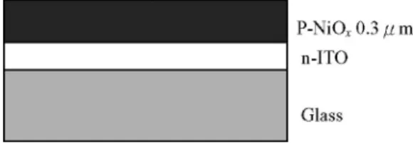
Figure 1 shows the schematic structure of the NiOx/ ITO/glass heterojunction diode. The NiOx films of
about 0.3m were deposited on the ITO glass by the reac-tive rf magnetron sputtering with different Ar/ O2 ratios in the chamber. The target was the NiO共99.99%兲 with a diam-eter of 3 in. The Ar/ O2ratios were 100/ 0, 100/ 36, 25/ 100, and 0 / 100 for samples共a兲, 共b兲, 共c兲, and 共d兲, respectively. The sheet resistance of the ITO glass was about 70⍀/䊐. The deposition was performed at a total pressure of 20 mTorr and a rf power of 200 W. The temperature of the ITO substrates was maintained below 60 ° C during sputtering. The x-ray 共Cu K␣兲 diffraction 共XRD兲 patterns of the NiOx films have
shown the first five peaks of the NiO lattice, which are iden-tical to the 2 peaks of cubic nickel oxide. The samples for TGA were obtained by scratching the films on the glass
a兲Author to whom correspondence should be addressed; electronic mail:
FIG. 1. A schematic structure of the NiOx/ ITO/glass heterojunction diode.
The sheet resistances of the ITO and NiOxare 70 and共6–18兲⫻106⍀/䊐,
respectively.
0021-8979/2006/100共12兲/124503/5/$23.00 100, 124503-1 © 2006 American Institute of Physics
共Corning 7059兲. Both the films on the glass and on the ITO glass were deposited at the same conditions. Measurements of TGA were conducted under normal conditions. TGA data were also used to determine the composition of x of the NiOx
films. In addition, XPS was performed to characterize the properties of NiOxfilms of the heterojunction diodes.
III. RESULTS AND DISCUSSION
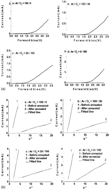
Figure 2 shows the I-V curves of the as-deposited NiOx/ ITO/glass heterojunctions at room temperature. The
characteristics of NDR can be observed to heavily depend on the ratios of sputtering gases Ar and O2during the deposition of NiOxfilms. From sample共a兲 to sample 共d兲, the
character-istics of the devices change from a rectifying diode to a diode with NDR, and both peak voltage and valley voltage increase. Apparently, the peak-to-valley current ratio共PVCR兲
Ip/ Iv also increases from 1 to 5 when the O2 in the gas mixture increases. In addition, the swing voltage Vs is
ap-proximately 1.05 V for every diode.
Figure3 shows the PVCR and turn-on voltage as
func-tions of the mixture ratio of O2/ Ar+ O2. Both the PVCR and the turn-on voltage increase as the mixture ratio of O2 in-creases. To realize the effect of O2 in the NiOx films, the
resistivity of the NiOxfilms was measured at room
tempera-ture and shown in TableI. Bransky and Tallan had reported the decrease of resistivity as the partial pressure of O2in the Ar– O2 mixture increases.12 The decreasing resistivity has been attributed to the excess O2in the NiOxfilms causing the
following reactions: 1
2O2→ OO+ VNi, 共1兲
VNi→ VNi
⬘
+ hole, 共2兲VNi
⬘
→ VNi⬙
+ hole, 共3兲where OOis an oxygen ion on the normal site, VNiis a nickel vacancy with two Ni3+ions next to the vacancy, and V
Ni
⬙
andVNi
⬙
are ionized vacancies with one and two electrons on the vacancy, respectively.7,12 Based on Eqs. 共2兲 and共3兲, excess O2 in the NiOx film enhances the concentration of hole anddecreases the resistivity. The increased hole concentration also increased the difference between the Fermi level of the
p-type NiOx and the fixed Fermi level of the n-type ITO.7
Due to the low voltage drop across the p-side NiOxand the
n-side ITO film, both built-in and turn-on voltages of the
NiOx/ ITO increased as the ratio of O2/ Ar+ O2 increased. Since ITO is a degenerate n-type semiconductor, the depleted region is mainly on the p-side of NiOxof the diodes.
Figure4共a兲shows the I-V curves of the NiOx/ ITO/glass
diodes annealed at 450 ° C in air for about 30 min. The char-acteristics of NDR disappeared and the charchar-acteristics of the rectifying diodes were observed. In the meantime, the trans-mittance of the rectifying diodes is over 60% and is about two times larger than the diodes with NDR at the visible region. The differential resistance also increases about ten times, from a few hundred ohms to a few thousand ohms. Sample 共d兲 has the lowest differential resistance of about 1000– 2000⍀. As a result of high differential resistance, turn-on voltage also shifts to a higher value of 1.6– 2.2 V. By investigating the I-V curves of Figs.4共a兲and2 at a for-ward bias larger than the turn-on voltage, the operation cur-rent is not similar to the rapidly rising diffusion curcur-rent in the conventional semiconductor p-n junctions. Instead, other factors dominate the current transport. This kind of I-V curves has been observed in the oxide-based p-n homojunc-tions and heterojunchomojunc-tions.13–16 In the homojunction, a linear
I-V has been attributed to a change of stoichiometry in the p
and n regions by increasing the voltage at high
temperature.13In our case, two different oxide-based materi-als NiOxand ITO formed a p-n heterojunction, and a change
of stoichiometry of NiOxand ITO at room temperature could
not occur. In an oxide-based p-n heterojunction, both the high series resistance and the space-charge-limited current FIG. 2. Room temperature I-V curves of the NiOx/ ITO/glass diodes
sput-tered with different gas mixing conditions before thermal annealing.
FIG. 3. Ratio of Ip/ Ivand turn-on voltage of the NiOx/ ITO/glass
hetero-junction diodes sputtered with different gas mixing ratios of O2/ Ar+ O2.
TABLE I. Resistivity of the NiOxfilms.
Ar/ O2ratio 100/ 0 100/ 36 25/ 100 0 / 100
Resistivity 共⍀ cm兲
653 303 333 170
124503-2 Chang et al. J. Appl. Phys. 100, 124503共2006兲
could be the reasons of this kind of I-V curve.4,14–16 The space-charge-limited current is proportional to 关共V2兲/共N
tl3兲兴exp共−Et/ kT兲, where, V, Nt, l, and Etare the
mobility of carriers, applied voltage, density of traps, thick-ness of the space charge layer, and energy level of traps, respectively.14,17,18 Figure 4共b兲 shows the I-V2 curves of samples 共a兲–共d兲 before and after annealing. Linear relations of I and V2 were obtained for all samples at room tempera-ture, while the forward bias voltage was larger than the turn-on voltage. The linear relation of I and V2indicates that the carrier transport in the NiOx/ ITO/glass heterojunction
diode is dominated by the space-charge-limited current. Since ITO is a metal-like n-type semiconductor, the region of the space-charge-limited current is mainly in the p-NiOx
re-gion. In Fig. 4共b兲, both space-charge-limited current and slope of I-V2 curves decrease after annealing, where the slope is a function of Nt, l, and Etat a fixed temperature.
To realize the changes in the characteristics of the
het-erojunction diodes before and after annealing, we inspect the characteristics of NiOxfilms by XPS, TGA, and AFM.
Fig-ure5shows the TGA profile of sample共d兲 and indicates that heating NiOxfilms leads to the loss of weight of NiOx
par-ticles. As the annealing temperature was below 300 ° C, the lost weight might be due to the oxygen release from the grain boundaries of nanosized NiO in the film. A clear transition appears at about 300 ° C, which implies a new compound but not NiO in the NiOxparticles because the decomposed
perature of NiO is over 550 ° C. While the annealing tem-perature is above 550 ° C, the decomposition stops and the weight is retained.
Figure6shows XPS spectra of the NiOxfilm before and
after annealing. XPS spectra show two peaks at 529.5 and 532 eV. The peak of 529.5 eV represents a binding energy of O 1s peak in the NiO and the peak of 532 eV represents a binding energy of O 1s peak in the Ni2O3, where a nickel ion in Ni2O3is Ni3+.19,20
It is known that a Ni3+ion is equivalent to an acceptor and a nickel vacancy in Eqs.共2兲and共3兲 con-necting two Ni3+ ions via a quadruple force.7
On the other hand, the increasing relative content of NiO in the film indi-cates a chemical process connecting NiO and Ni2O3 while the NiOxfilm is annealed. Based on the TGA results, heating
causes the black NiOx particles to decompose and change
into green particles finally. Combining the results of TGA and XPS, the decomposed compound Ni2O3via a reaction of Ni2O3→2 NiO+12O2 or a reaction of NiOx→NiO+共x
− 1兲/2 O2 in the film can produce green NiO particles and O2. Based on Le Châtelier’s principle, releasing O2in Eq.共1兲 FIG. 4.共a兲 I-V curves of the samples 共a兲, 共b兲, 共c兲, and 共d兲 after annealing at
450 ° C in air for about 30 min. Measurements were conducted at room temperature. 共b兲 I-V2curves of the annealed and unannealed samples at
forward bias larger than the turn-on voltage.
FIG. 5. Thermogravimetric analysis profile of the sample共d兲.
FIG. 6. X-ray photoelectron spectrum of the sample 共d兲 before and after annealing.
causes the concentration of holes or Ni3+ ions to decrease, which is responsible for the increase of the resistance and turn-on voltage of the heterojunction diodes. Besides, the Ni3+ion is also a color center in the film,21where the lower concentration of Ni3+ions increases the transmittance of rec-tifying diodes.
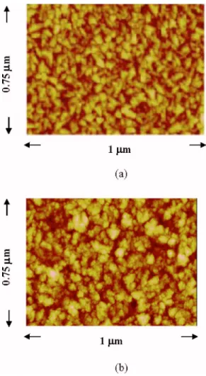
Figures7共a兲and7共b兲show the AFM images of the NiOx
film on the ITO glass before and after annealing, respec-tively. In Fig.7共a兲, the film composed of grains with size of about 30 nm shows clear boundaries. The XRD analysis in-dicated that crystallite NiO was embedded in the grains and TGA showed the excess oxygen in the film. On the other hand, XPS showed two states of oxygen in the film, i.e., NiO and Ni2O3. The results of XRD and XPS indicated that the excess oxygen had to be located between grain boundaries of NiO forming VNi
⬘
and VNi⬙
vacancies, as shown in Eqs. 共2兲 and共3兲. As is well known, semiconductor grain boundaries formed a double Schottky barrier with a space-charge region along the boundaries.22In Fig.4共b兲, the space-charge-limited current is the evidence that holes transport across the bound-ary region. In Fig.7共b兲, the grain structure of NiOxis similarto Fig.7共a兲, but the shape of the grains is different and the size of the grains increases. The space between grain bound-aries was also enlarged when the sample was annealed. The increased size of the crystallite NiO was consistent with the XRD analysis that the full width at half maximum共FWHM兲
of NiO 2 peaks was narrowed. The increased grain size could be the result of grains merging together due to the excess oxygen released between grain boundaries. After oxy-gen was released, the decreased hole concentration caused the space-charge-limited current and slopes shown in Fig.
4共b兲 to decrease since the space-charge-limited current is proportional to free carriers.17
Since the energy states of VNi
⬘
in the NiOxwere higherthan the Fermi level,7 the property of the NiOx was
analo-gous to a p+-type共degenerate兲 semiconductor. Therefore, the
p+-n+ heterojunction structure of NiOx/ ITO/glass could be
the cause NDR at small forward bias since the electrons at the ITO side could tunnel to the finite energy states of VNi
⬘
. After oxygen was released from the NiOxfilm, the decreasedconcentration of VNi
⬘
, as shown in Eq.共2兲, caused the disap-pearance of the NDR.Results of TGA, XPS, AFM, and XRD indicated that oxygen in the NiOxfilm was responsible for the
characteris-tic changes. Furthermore, the depleted region of the diode was mainly on the NiOxlayer. Therefore, decreasing oxygen
content in the NiOxlayer leads both to the disappearance of
NDR characteristics and to the decrease in the space-charge-limited current as well as the slope of the I-V2. In the mean-time, the diodes with higher transmittance and higher differ-ential resistance are also due to the released oxygen content. IV. CONCLUSIONS
p-NiOx/ n-ITO/glass heterojunction diodes were
demon-strated. The ratios of sputtering gaseous Ar and O2during the NiOxfilm were formed and heavily changed the
characteris-tics of the heterojunction diodes from rectifying diodes to diodes with NDR. After annealing at 450 ° C in air for about 30 min, all diodes showed properties with higher transmit-tance and differential resistransmit-tance in comparison with the di-odes before annealing. Linear I-V2curves indicated that the space-charge-limited current dominates the current transport in the NiOxlayer. By analyzing the properties of NiOxfilms
with XPS spectra, TGA data, and AFM image, the released oxygen in the NiOxfilms was found to be responsible for the
disappearance of NDR characteristics and the for the change of the nonideal rectifying diode characteristics. The results should be useful and helpful in optimizing the process of the transparent oxide-based heterojunction diodes.
ACKNOWLEDGMENTS
This work was supported in part by the National Science Council of the Republic of China 共ROC兲 in Taiwan under Contract No. NSC93-2120-M-009-006 and by the Academic Excellence Program of the ROC Ministry of Education under Contract No. NSC93-2752-E-009-008-PAE.
1N. Miura, J. Wang, M. Nakatou, P. Elumalai, and M. Hasei, Electrochem.
Solid-State Lett. 8, H9共2005兲.
2H. Ohta, K. Kawamura, M. Orita, M. Hirano, N. Sarukura, and H. Hosono,
Appl. Phys. Lett. 77, 475共2000兲.
3R. L. Hoffman, B. J. Norris, and J. F. Wager, Appl. Phys. Lett. 82, 733
共2003兲.
4X. L. Guo, J. H. Choi, H. Tabata, and T. Kawai, Jpn. J. Appl. Phys., Part
2 40, L177共2001兲.
5H. Ohta, M. Hirano, K. Nakahara, H. Maruta, T. Tanabe, M. Kamiya, T.
FIG. 7. 共Color online兲 共a兲 AFM images of the sample 共d兲 before annealing and共b兲 after annealing.
124503-4 Chang et al. J. Appl. Phys. 100, 124503共2006兲
Kamiya, and H. Hosono, Appl. Phys. Lett. 83, 1029共2003兲.
6W. Y. Lee, D. Mauri, and C. H. Wang, Appl. Phys. Lett. 72, 1584共1998兲. 7D. Adler and J. Feinleib, Phys. Rev. B 2, 3112共1970兲.
8A. Kudo, H. Yanagi, K. Ueda, H. Hosono, and H. Kawazoe, Appl. Phys.
Lett. 75, 2851共1999兲.
9H. Kawazoe, M. Yasukawa, H. Hyodo, M. Kurita, H. Yanagi, and H.
Hosono, Nature共London兲 389, 939 共1997兲.
10A. Kudo, H. Yanagi, H. Hosono, and H. Kawazoe, Appl. Phys. Lett. 73,
220共1998兲.
11H. Sato, T. Minami, S. Takata, and T. Yamada, Thin Solid Films 236, 27
共1993兲.
12I. Bransky and N. M. Tallan, J. Chem. Phys. 49, 1243共1968兲. 13I. Riess, Phys. Rev. B 35, 5740共1987兲.
14M. Sugiura, K. Uragou, M. Tachiki, and T. Kobayashi, J. Appl. Phys. 90,
187共2001兲.
15T. Nakasaka, K. Urago, M. Sugiura, and T. Kobayashi, Jpn. J. Appl. Phys.,
Part 2 40, L518共2001兲.
16G. Z. Yang, H. B. Lu, F. Chen, T. Zhao, and Z. H. Chen, J. Cryst. Growth
227–228, 929共2001兲.
17A. Rose, Phys. Rev. 97, 1538共1955兲. 18R. H. Jarman, J. Appl. Phys. 60, 1210共1986兲.
19A. Agrawal, H. R. Habbi, R. K. Agrawal, T. P. Cronin, D. M. Roberts, S.
Caron-Popowich, and C. M. Lampert, Thin Solid Films 221, 239共1992兲.
20K. S. Kim and N. Winograd, Surf. Sci. 43, 625共1974兲.
21M. Kitao, K. Izawa, K. Urabe, T. Komatsu, S. Kuwano, and S. Yamada,
Jpn. J. Appl. Phys., Part 1 33, 6656共1994兲.
22C. R. M. Grovenor, J. Phys. C 18, 4079共1985兲.