國 立 交 通 大 學
光 電 工 程 研 究 所
碩 士 論 文
氧化銦錫薄膜與奈米結構兆赫頻段
光學特性之研究
Terahertz spectroscopic studies of
ITO thin films and nanostructures
研 究 生:林晏徵
指導教授:潘犀靈 教授
氧化銦錫薄膜與奈米結構兆赫頻段光學特性之研究
Terahertz spectroscopic studies of ITO thin films
and nanostructures
學生:林晏徵 Student: Yen-Cheng Lin 指導教授:潘犀靈教授 Advisor: Prof. Ci-Ling Pan
國立交通大學
光電工程研究所
碩士論文
A Thesis
Submitted to Department of Photonics and
Institute of Electro-Optical Engineering
College of Electrical Engineering
National Chiao Tung University
In partial Fulfillment of The Requirements
For The Degree of Master of Science
In
Electro-Optical Engineering
July 2009
Hsinchu, Taiwan, Republic of China
氧化銦錫薄膜與奈米結構兆赫頻段光學特性之研究
學生:林晏徵 指導教授:潘犀靈教授國立交通大學研究所
摘要
我們使用富立業遠紅外光光譜以及兆赫波時域光譜的光學量測方法去探討氧 化銦錫薄膜及氧化銦錫奈米柱的光學特性和電性。且對於不同厚度的薄膜(189nm ~ 961nm),我們得到以下的特性: 樣品之電漿頻率隨著厚度變厚而變大,其值 1600(rad.THz)到 1950 (rad.THz)。 以 Drude 的自由載子模型的知載子散射時間為 6~7(fs)。且我們也同樣得到對 應的載子漂流率跟載子濃度,分別為 32~34(cm2 /Vs)和(2.8~4.2)×1020 。我們得 到的這些電性結果可以跟霍爾量測到的結果做相對應的比較,且得到相近的數 值。 同樣的,我們可以將這光學量測技術使用於奈米結構樣品的探討。在本論文 裡面,我們將研究氧化銦錫的奈米柱結構,並引進 Drude-Smith 模型及等校介值 理論來輔助分析。ii
Terahertz spectroscopic studies of ITO thin films
and nanostructures
Student: Yen-Cheng Lin Advisor: Prof. Ci-Ling Pan
Department of Photonics and Institute of Electro-Optic Engineering, College of Electrical Engineering National Chiao Tung University
Abstract
We investigate the optical and electrical properties of Indium Tin Oxide (ITO) thin film and Indium Tin Oxide (ITO) nanocolumns with the optical characterization methods including Fourier Transform Infrared Spectroscopy (FTIR) and Terahertz Time Domain Spectroscopy (THz-TDS). For different thicknesses of the Indium Tin Oxide (ITO) thin films (189nm~961nm), the plasma frequencies are determined to be from 1600 (rad.THz) to 1950 (rad.THz), and scattering times are in the range of 6~7 fs based on the free electron Drude model. The mobilities of the above Indium Tin Oxide (ITO) thin films are determined to be 32~34cm2/Vs. The carrier concentration is verified to be in the range of (2.8~4.2)×1020. The electrical properties of the thin films derived from non-contact optical techniques agree well with those determined by the conventional Hall measurement.
Similarly, the techniques are also introduced to the nanostructure materials, Indium Tin Oxide (ITO) nanocolumn. We study the optical and electrical properties of the sample with the Drude-Smith model and the effective medium approximation (EMA) which are demonstrated in the thesis.
致謝
兩年的碩班生活即將結束了!在這要先感謝一起修課的同學們,沒有你們的 陪伴,我是當不了早起的鳥兒的。因為有你們,我的修課生活變得很精彩。 就算畢業了,也一定不會忘記實驗室的同仁們的,因為大家給的指導跟關心, 是我做研究得動力。且這篇碩論之所以能完成,完全都要感謝 Moya 學長亦師亦 友的指導,以及 Mika 學長的經驗傳承跟 Tiger 的問題討論,還有山哥及猛哥的 巧手教學及冠儒學弟的實驗幫忙等等。沒有你們或許我會念碩士真得要念碩四 了! 最後要感謝的是我的家人,沒有你們的支持,我想我是很難度過最後難關的。 尤其是妹妹芝嶸更是在我百忙之際時雪中送炭!謝謝你們,最愛你們了!iv
Contents
摘要
... iAbstract
……….ii致謝
………...iiiContents
………ivList of Figures
………...viList of Tables
………...ixChapter 1 Introduction
1-1
THz introduction
……….11-2 Transparent Conductive Oxides ………..3
Basic introduction of PV Solar Cell ………3
TCOs of PV Solar Modules ………4
ITO Film from NDL ………6
ITO Nanocolumn from Prof. Yu ………...9
1-3 Motivation
………...11Chapter 2 Models and Analysis Methods
2-1 Models in Our Analysis
………..12Macroscopic Fields and Maxwell’s Equations ……….12
Propagation of Light in Isotropic Dielectrics ………13
Propagation of Light in Conducting Media ………..15
Drude Smith Model ………...17
2-2 The Method of Measurement and Data Analysis
……….19Thin Film Sample ……….19
Theoretical transmission formula ……….19
Refraction index extraction ………...21
2-3 Effective Medium Approximation
………....26Depolarization Field ………...26
Local Electrical Field ………....27
Clausius-Mossotti relation ………29
Heterogeneous Dielectric and Effective-Midium Theory ……….30
Chapter 3 Experimental Result and Discussion of ITO Thin Film
3-1 Characters of Samples
……….32ITO Thin Film (with O2 flux) ………....32
Optical Spectroscopy of ITO Thin Film ………...35
Reflection Type Far Infrared Spectroscopy(R-FTIR) ………...36
Hall Measurement ……….38
3-2 Reflection Type FTIR using Drude Model fitting
………39Fitting Model and Reflectance FTIR Spectroscopy ………..40
3-3 THz Time Domain Spectroscopy
……….48System Set Up ………...48
Data Analysis ………....49
The physical diagrams of our measurement ………..61
Chapter 4 Experimental Result of ITO nanocolumn
4-1 Characters of ITO nanocolumn and motivations
……….63ITO nanocolumn (with N2 flux) ………63
4-2 Data Analysis
……….64FTIR spectroscopy ………64
FTIR data fitting ………....65
THz-TDS: (Transmission Type) ………....67
Discussion: Comparison of THz-TDS and FTIR measurements …………..71
Chapter 5
Conclusion
……….75vi
List of Figures
1-1-1 The spectral range of electromagnetic waves
(http://www.rpi.edu/terahertz/about_us.html) ... 2
1-2-1 The p-i-n type thin film silicon solar cell with light incident …………... 5
1-2-2 Rough surface of TCO and back reflector to increase the light absorption ……….. 5
1-2-3 Film with thickness 961.6(nm) ………... 7
1-2-4 Film with thickness 483.0(nm) ………... 7
1-2-5 Film with thickness 188.9(nm) ………. 8
1-2-6 The picture of the chamber (ITO nanocolumns) ………... 9
1-2-7 A cutaway view of the chamber (ITO nanocolumns) ………. 10
1-2-8 SEM image of ITO nanocolumns deposited with obliquely incident with nitrogen flux ………... 10
2-2-1 The Diagram of the reference (THz exp.) ……….. 20
2-2-2 The Diagram of the sample (THz exp.) ……….. 20
2-2-3 The flow chart of the n κ value extraction (THz exp.) ………... 22
2-2-4 The flow chart of the conductivity value extraction (THz exp.)………. 25
2-3-1 Depolarization field E1 tends to oppose the applied field E0 …………... 27
2-3-2 Electric fields act on the center of the ellipsoid on the site of an atom ………... 28
2-3-3 Calculation of the field in a spherical cavity in a uniformly polarized medium ………... 29
3-1-1 Film with thickness 961.6(nm) ………... 32
3-1-2 Film with thickness 483.0(nm) ………... 33
3-1-3 Film with thickness 188.9(nm) ………... 33
3-1-4 The electron scattering at the grain boundary and the ionized impurity ……….. 34
3-1-5 Spectra of JASCO: V-670 spectrometer (transmission type) for thin ITO films of the different thickness: 961.6nm, 483.0nm, and 188.9nm ……….. 36
3-1-6 FTIR of ITO film at short wavelength range with lower reflection part
……….. 37
3-1-7 FTIR of ITO film at long wavelength range with higher reflection part (The horizontal axis is in log scale.) ………... 37
3-2-1 Spectra of ITO film by reflection type FTIR (400 cm-1 to 7500 cm-1) ……….. 40
3-2-2 It shows how to get the plasma frequency, and carrier scattering time from FTIR spectra ………... 42
3-2-3 Fitting curve of ITO film with thickness 188.9nm ………. 43
3-2-4 Fitting curve of ITO film with thickness 483.0nm ………. 44
3-2-5 Fitting curve of ITO film with thickness 961.6nm ………. 45
3-3-1 Antenna THz time domain spectroscopy system ………... 48
3-3-2 THz waveform transmits through ITO film with thickness 188.9nm ……….. 49
3-3-3 THz frequency domain spectra of TO film with thickness 188.9nm ……….. 50
3-3-4 The refraction index of TO film with thickness 188.9nm ………...51
3-3-5 σ(ω) of TO film with thickness 188.9nm ……….…51
3-3-6 THz waveform transmits through ITO film with thickness 483.0nm ……….. 52
3-3-7 THz frequency domain spectra of TO film with thickness 483.0nm ………..….53
3-3-8 The refraction index of TO film with thickness 483.0nm ………...….54
3-3-9 σ(ω) of TO film with thickness 483.0nm ………... 54
3-3-10 THz waveform transmits through ITO film with thickness 961.6nm ……….. 55
3-3-11 THz frequency domain spectra of TO film with thickness 961.6nm ………. ….56
3-3-12 The refraction index of TO film with thickness 961.6nm …... 57
3-3-13 σ(ω) of TO film with thickness 961.6nm ……….. ……..57
3-3-14 Compared the frequency domain spectra of the ITO thin films ……….. 58
3-3-15 Compared the refractive index of the ITO thin films ………. ….58
3-3-16 Compared the conductivity of the ITO thin films ………... 58
viii
4-1-1 SEM of ITO nanocolumn ………... 63
4-2-1 FTIR of ITO nanocolumn at low wavelength part ……….. 64
4-2-2 FTIR of ITO nanocolumn at high wavelength part ………. 64
4-2-3 Fitting curve of ITO nanocolumn (FTIR exp.) ………... 66
4-2-4 The THz TDS spectroscopy of ITO nanocolumn ………... 67
4-2-5 The frequency domain spectroscopy of ITO nanocolumn ………..…….68
4-2-6 The refraction index of ITO nanocolumn in THz range ………. 69
4-2-7 Theσ(ω) of ITO nanocolumn in THz range ………...70
4-2-8 Refraction index of ITO nanocolumn from FTIR and THz-TDS ……….. 72
4-2-9 Conductivity of ITO nanocolumn from FTIR and THz-TDS ……….. 73
List of Tables
2-3-1 the depolarization factors for the body with different shapes
………. 27
3-1-1 ITO thin film electric properties measured by Hall measurement ………... 38
3-1-2 The sheet resistivity of Hall measurement compared with 4-point probe measurement ……….. 39
3-2-1 Fixed parameters (FTIR fitting) ………. 43
44
45
3-2-2 Fitting parameters of ITO film 188.9nm (FTIR fitting) ……….... 43
3-2-3 Fitting parameters of ITO film 188.9nm (FTIR fitting) ……….... 44
3-2-4 Fitting parameters of ITO film 961.6nm (FTIR fitting) ……….45
3-2-5 Fitting parameters of ITO film, 961.6nm, 483.0nm, and 188.9nm compare with the Hall measurement ………...47
3-3-1 Compared THz-TDS, Hall, and FTIR with the optical and electrical parameters ……….. 60
4-2-1 Fixed value (FTIR fitting for nanocolumn )………... 66
4-2-2 Calculated from the model fitting of FTIR (FTIR fitting for nanocolumn ) ………. ….66
1
Chapter 1 : Introduction
1-1 Introduction of THz
Terahertz (THz) radiation lies in the frequency gap between the infrared and microwaves(see Fig. 1-1-1), typically is referred to as the frequencies from 100 GHz to 30 THz. 1 THz is equivalent to 33.33cm-1 (wave numbers), 4.1 meV photon energy, 300μm wavelength. Before 1980s people don’t know much about THz because the generation and detection technologies are not well established, but since the development of femtosecond laser, THz has been intensely studies. At middle 1980s, Auston [1] successfully used photoconductive dipole antenna to generate and detect coherently THz radiation in time domain, and this technology is called THz time-domain spectroscopy (THz-TDS). After Auston’s research many other generation methods have been developed including optical rectification [2], surge current in semiconductor surface [3], quantum cascade laser [4]…, and in 1995 XC-Zhang et al[5] successfully used ZnTe crystal to detect THz radiation by free-space electro-optic sampling that highly increased the detection bandwidth and signal to noise ratio.
Fig.1-1-1 The spectral range of electromagnetic waves (http://www.rpi.edu/terahertz/about_us.html)
Terahertz has much smaller photon energy (4.1 meV) compared to X-ray and therefore this kind of non-destruction measurement can be used for biology and medical sciences [6]. Image and tomography [7] of THz have also been studied and can be applied to homeland security.
For semiconductors measurement, conventional four point probe and Hall effect measurement can measure the characteristics including mobility, carrier concentration and resistivity of the semiconductor materials by direct sample contact. All these electrical measurements measure only DC value of the sample but some characteristics, including refractive index, conductivity, are frequency-dependent. For some semiconductors with high resistivity and low concentration, the electrical properties are difficult to be measured by simple direct contact because at the metal-semiconductors interface, the Schottky barrier may disturb the measurement value. Therefore, THz-TDS with advantages of non-contact and frequency-dependant measure is desirable for semiconductors characterization. In 1990 D. Grischkowsky et
3
GaAs, other semiconductors such as silicon [9] have also been widely studied. Recently, many nanostructured semiconductors like InP-nanoparticle [10], ZnO-nanowire [11], Si-nanoparticle [12] have been studied using THz-TDS technology and the particular conduction behavior have been observed. In comparison with conventional far-IR source and detector, THz-TDS is a coherent technology that means both amplitude and phase information can be obtained. Both absorption coefficient and refractive index could be extracted without use of Kramers-Kronig relation that simplifies the analysis process.
1-2
Transparent Conductive Oxides (TCOs)
Basic introduction of PV Solar Cell
Nowadays, solar cells have become essential devices because of the energy crisis. The major and subsequence field of studying solar modules become the top topic of the Green-energy because of the shortage of petroleum and coal which are the powerful and useful energy sources creating a successfully prosperous industry world in nineteenth and twentieth century.
The quest for low-cost, high-effective, sustainable energy source is one of the prior concerns of the industrial society at the present age. Photovoltaic solar energy is the major part in this quest. The main reason is related to their manufacturing cost, to their market price. This kind of thin film photovoltaic solar cell can be deposited on low-cost large-area substrates. Various semiconductors, compound semiconductors, have been invested for thin film solar cell such as CdTe and Cu (In, Ga)Se2 (CIGS) have attracted much attention in the past research, because of relatively high laboratory efficiencies. For the low cost purpose, the thin film silicon solar cell manufacturing is the best choice.
TCOs of PV Solar Modules
Thin film silicon solar cells, consisting of amorphous and microcrystalline silicon which have the relatively low value of absorption coefficient, need elaborate light-trapping schemes in order to absorb a sufficient part of incoming solar spectrum, within reasonable thickness to ensure satisfactory efficiencies. In a solar cell, to increase the photo-generation and short circuit current density, all reflection and absorption losses have to be minimized. It means as below:
(a.) AR coating might be used on the solar module where light enters into it. (b.) Back reflectors necessarily have as little absorption as possible
(c.) The substrate and the front TCO layer must have high transparency at 300 to 1200 nm, the solar spectral range.
(d.) TCO layers and the layers which do not contribute to photo-generation and collection, should be kept as thin as possible and have very low absorption coefficient in the acting spectral range.
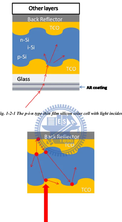
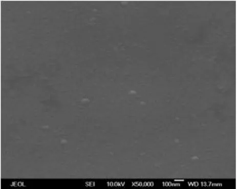
Fig. 1-2-1 and 1-2-2 show the diagrams, that light propagate in the solar cell. With the rough surface of the TCO layers, the sunlight is widely scattered and improving the absorption at the silicon layers which transverse the light energy to the electrical energy. And in the diagram, it also shows the benefit of the back reflector, which reflects the light to confine the propagating light. [13][14]
5
Fig. 1-2-1 The p-i-n type thin film silicon solar cell with light incident
TCO layers are used as a front electrode and as part of the back side reflector in the solar module. When it applied at the front side, there are few properties should followed:
(a.) High transparency ( in the spectral rang where solar cell is operating). (b.) High conductivity
(c.) Strong scattering of the incoming light into Si absorber layer.
(d.) To be favorable physical-chemical properties for the growth of the silicon.
ITO Film from NDL:
ITO thin films with thickness as followed, 961.6nm, 483.0nm, and 188.9nm, are prepared by NDL with the DC reactive magnetron sputtering. The growth conditions are shown below:
1. vacuum pressure: 6 m-torr 2. sputtering power: 300W
3. growth on fused silica, the substrate 4. substrate temperature: 250˚C
5. with O2 and Ar
By using the commercial machine, Ulvac DC sputter, with target compositions are 90 wt% In2O3 +10 wt% SnO2 and purity of it is 99.99 wt% manufactures the ITO thin
7
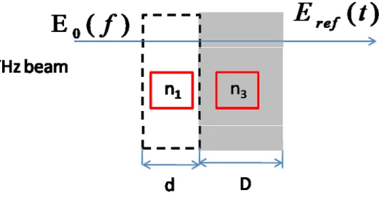
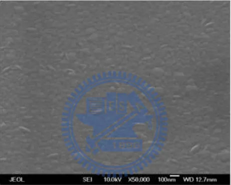
The morphology of the ITO thin film: (the surface roughness and the grain) Fig. 1-2-3 ~ 1-2-5 are shown in the SEM photography.
Fig. 1-2-3 Film with thickness 961.6(nm)
Fig. 1-2-5 Film with thickness 188.9(nm)
The Fig.1-2-3 to 1-2-5 show the top views of our ITO film samples. The magnification is ×50,000. The pictures with a scale 100nm make us find out the grain size of each sample. Therefore, we have the grain size, 30nm, 20nm, 10nm for the sample with thickness, 961.6nm, 483.0nm, 188.9nm, respectively.
9 ITO Nanocolumn from Prof. Yu
ITO nanoculumn with thickness 1µm is grown under the following conditions:
1. deposition angle: α~70˚ 2. vacuum pressure: 10-4 torr 3. growth on Si cell
4. substrate temperature: 240˚C 5. with N2
Using the commercial target compositions are 95 wt% In2O3 + 5 wt% SnO2.
The chamber diagrams are shown below: Fig.1-2-6 and Fig.1-2-7
Fig. 1-2-7 A cutaway view of the chamber
Fig. 1-2-8 SEM image of ITO nanocolumns deposited with obliquely incident with
Vacuum
pump
Normal
Line
ITOφ
C H A M B E R
Holder
θ
11
1-3 Motivation
The THz region is ideal for probing semiconductors because the frequency range closely matches typical carrier scattering rates of 1012 to 1014 (Hz).
Therefore, we introduce the optical characterization techniques including FTIR and THz-TDS to measure our samples, ITO thin films and ITO nanocolumn, prepared by NDL and Prof. Yu’s group, respectively. It is a non-contact probe method that could avoid destroying our sample surface. By optical analysis with Drude and Drude Smith model, we also could get the electric properties, such as DC mobility, DC conductivity and carrier concentration.
We will introduce the effective medium theory to the nanostructure sample. In the scale around the atom site, the localized field cannot be ignored. And it is a very interesting topic for the physical phenomenon.
Chapter 2 : Theoretical and experimental
methods
2-1 Analysis Models
Macroscopic Fields and Maxwell’s Equations:
The electromagnetic state of matter at a given point is described by four quantities:
(1). the volume density of electric charge ρ
(2). the volume density of electric dipoles, called the polarization P
(3). the volume of density of magnetic dipoles, called the magnetization M (4). the electric current per unit area, called the current density J
All of these quantities are considered to be macroscopically averaged to smooth out the microscopic variations due to the atomic makeup of all matter. The relations of the macroscopically averaged field E and H are described as following by Maxwell equations: z E= 0 H 0 M t t μ ∂ μ ∂ ∇× − − ∂ ∂ => E= B t ∂ ∇× − ∂ --- (2-1-1) z H= 0 E+ P+J t t ε ∂ ∂ ∇× ∂ ∂ => H= D J t ∂ ∇× + ∂ --- (2-1-2) z 0 0 1 E= P ρ ε ε ∇ • − ∇ • + => ∇ •D=ρ --- (2-1-3) z ∇ •H = −∇ •M => ∇ •B=0 --- (2-1-4)
13
0
D=ε E+P= Eε , called the electric displacement --- (2-1-5)
0( )= H
B=μ H+M μ , called the magnetic induction --- (2-1-6)
In our case, we separate bound charge and bound current from free charge and free current. This separation is more useful for calculations involving dielectric materials.
z E= B t ∂ ∇× − ∂ --- (2-1-7) z H= f D J t ∂ ∇× + ∂ --- (2-1-8) z ∇ •D=ρf --- (2-1-9) z ∇ •B=0 --- (2-1-10)
Propagation of Light in Isotropic Dielectrics: [16]
The electrons are permanently bound to the atoms comprising the medium of a non-conducting, isotropic medium. Assume that each electron, of charge -e, has a displaced distance r from its equilibrium position. The macroscopic polarization P of medium is given by P = -Ner, where N(tilted) is the number of electrons per unit volume. Apply a static electric field E, the restoring force of electron is –eE=κr. If the electric field varies with time, the motion of equation with the damping term is
. .. ; eE κr m rγ m r − − − = 2 ( + ) ; eE ω m i mω γ κ r ⇒ − = − − --- (2-1-11)
Consequently, the polarization is given by 2 2 2 2 2 0 / P=- erN Ne E Ne m E; mω i mω γ κ ω ω iωγ = = − − + − − 0 m κ ω = , --- (2-1-12)
where ω0 is the effective resonance frequency of bound electrons.
To show how the polarization affects the propagation of the light, we return the the general wave equation derived from Maxwell’s equation.
2 2 0 0 2 2 2 1 ( E)+ E P J , c t μ t μ t ∂ ∂ ∂ ∇× ∇× = − − ∂ ∂ ∂ --- (2-1-13) In the above wave equation, the polarization term is important for non-conductive medium. On the other hand, the conduction term dominates for the metals. Considering ▽•E=0 and equation 2-1-13, we have
2 2 2 2 2 2 2 0 0 1 1 (1 Ne ) E; E c mε ω ω iγω t ∂ ∇ = + − − ∂ --- (2-1-14)
To seek a solution of the form
( ) 0 i z t . E E e Κ −ω
⎡ = ⎤
⎣ ⎦
It’s called homogeneous plane harmonic waves. The possible solution is provided
2 2 2 2 2 0 0 1 ( ) (1 Ne ); c m i ω ε ω ω γω Κ = + − − c . ω ⎡Κ = Ν⎤ ⎢ ⎥ ⎣ ⎦ 2 2 2 2 0 0 1 (n i ) 1 Ne ( ). m i κ ε ω ω γω ⇒ Ν = + = + − − --- (2-1-15)
15
Propagation of Light in Conducting Media: (free electron gas) [16]
S
ince the conduction electrons are not bound, there is no elastic force involved. We only consider the electron scattering inside the motion of equation as the form:1 d v m m v eE dt τ − + = − ( mτ
-1 is the frictional dissipation constant ) --- (2-1-16)
The current density is J=-Nev, N is the number of conduction electrons per unit volume. The equation can be derived as followed:
2 1 d J Ne J E dt τ m − + = --- (2-1-17) (1.) Homogeneous solution: 1 0, d J J dt τ − + = The solution of it is:
/ 0 t
J =J e− τ, τ is called the relaxation time.
For a static electric field,
2 1 Ne J E m τ− = (J=σ 0E), 2 0 ; Ne m σ = τ --- (2-1-18)
(2.) With harmonic time variation field E (e-iωt):
2 1 1 0 (-i + )J Ne E E, m ω τ− = =τ σ−
From above equation we get the current density as the form:
0 , 1 J E i σ ωτ = −
Here we also introduce J=σE in our assumption. We have
0 ( )= ; 1 i σ σ ω ωτ
We also introduced the result to the general wave equation, and the equation is reduced to
--- (2-1-20)
We also take the simple homogeneous plane-wave solution as our trial solution.
( ) 0 i z t . E E e Κ −ω
⎡ = ⎤
⎣ ⎦
It is easily found that K must satisfy the relation
2 2 0 0 2 1 , i c i ωμ σ ω ωτ Κ = + − c . ω ⎡Κ = Ν⎤ ⎢ ⎥ ⎣ ⎦ --- (2-1-21)
In the condition of very low frequency, the formula is reduces to the approximate formula
2
0 0,
iωμ σ
Κ ≈ Κ ≈ iωμ σ0 0 = +(1 )i ωμ σ0 0 / 2; --- (2-1-22)
In the low frequency case, the real and imaginary parts of K are equal. (K=k+iα), k≈ ≈α ωμ σ0 0/ 2. --- (2-1-23)
Similarly, the real and imaginary parts of N are equal too. (N=n+iκ), n≈ ≈κ σ0/ 2ωε0 . --- (2-1-24)
Without the assumption, we drive the complex refraction index from the relation of K.
2 2 2 1 1 p , i ω ω ωτ− Ν = − + plasma frequency: 2 2 0 0 0 p c Ne m μ σ ω ε τ = = . --- (2-1-25) 2 2 0 0 2 2 1 ; 1 E E E c t i t μ σ ωτ ∂ ∂ ∇ = + ∂ − ∂
17 Drude Smith Model: [17]
While THz is widely used in Chemistry research and measurements of the conductivity of semiconductor, the flexibility Drude model have been invested in THz region. Better fits model are in the form of modified Lorentzians
0 1 ( )= , [1 (i ) ]α β σ σ ω ωτ − − --- (2-1-26)
where the exponents 1-αand βare treated as disposable parameters. With α=0 and β=1, we have the Drude result. With β=1 and α setting as variables is called the Cole-Cole(CC) model. With α=0 and varying the value of β, it is called the Cole-Davidson(CD) model. Some well-fit results were published in the past literature, such as:
On doped Si, Grischkowsky et al. report success with CD model and in transient photoconductivity measurements on GaAs, Schmuttenmaer et al. report success with keeping both α and β as varying parameters.
The formula with Lorentzian form requires that the frequency dependent conductivity should have the maximum at the zero frequency and then fall off. Departure phenomena have been observed, and we have to concern with those materials in which σ(ω) displays a minimum at zero frequency and a transfer of oscillator strength to higher frequencies in the form of an impulse response.
Let us introduced a simple impulse response approach to the optical conductivity, we have the initial current decays exponentially to its equilibrium value with a relaxation time τ as the form
( ) ( ) , (0) t j t e j τ − = --- (2-1-27)
and 2 1 ( )= ( ); 1 Ne m i τ σ ω ωτ − --- (2-1-28)
It is the form of Drude model. Then let us assume that an electron experiences collisions that are randomly distributed in time but with an average time interval τ between collision events. We have the resulting current response
( ) 1 ( ) ( ) [1 . ], (0) ! n t n n t j t e c j n τ ∞ τ − = = +
∑
--- (2-1-29) And 2 1 1 ( )= ( )[1 ]; 1 (1 ) n n n c Ne m i i τ σ ω ωτ ωτ ∞ = + −∑
− --- (2-1-30)This generalized Drude formula is called Drude Smith model following the name of the inventor, Smith. The coefficient cn represents the fraction of the electron’s original
velocity that is retained after the nth collision. In order to simplify our calculation, we
assume that the persistence of velocity is retained for only one collision (cn=0, for
n>1). We have the current response
( ) ( ) [1 ], (0) t j t ct e j τ τ − = + --- (2-1-31) and 2 1 ( )= ( )[1 ]; 1 1 Ne c m i i τ σ ω ωτ + ωτ − − --- (2-1-32)
For elastic collisions, c would be <cosθ> where θ is the scattering angle. The most important character of c is described as followed: When c is a negative value, it implies a predominance of backscattering.
19
2-2 The Method of Measurement and Data Analysis
Thin Film Sample (Transmission Type THz-TDS)
Considering a thin film with a thickness below 150µm, the time delay of it will be smaller than 1ps which is the duration of THz pulse. We cannot distinguish the second reflection from the main pulse. Therefore we introduce the multi-beam interference in our analysis as that to extract the information from the THz waveform by Fourier transform method (time domain to frequency domain). And then, we take the refraction index of substrate as a constant value to simplify the analysis method. (In practical, we use low absorption and constant refraction index material in THz range.)
Theoretical transmission formula
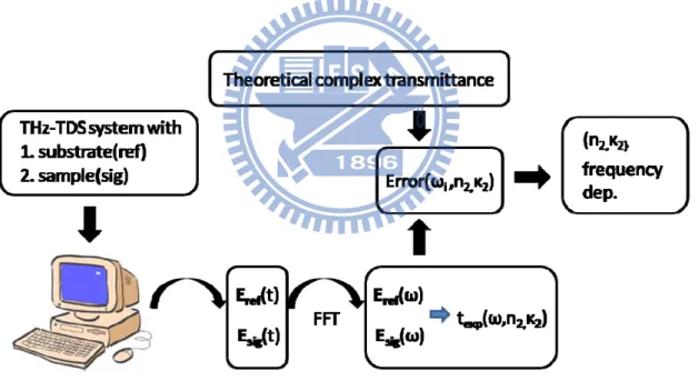
E0(ω) is the incident THz field, Eref(ω) is the reference electric field gone
through both the substrate ( the thickness is “D” ) and a bunch of air with thickness “d”, and Esig(ω) is the signal electric field transmitted through both the thin film ( the
thickness is “d” ) and the substrate ( the thickness is “D” ). We could write down the reference and signal field in the form of E0:
* 3 ( D) 13 31 0 ( ) ( ) ; n d i c ref E t t E e ω ω = ω + --- (2-2-1) * E ( ) 31 ( ) 3 ; n D i c sig t Efilm e ω ω = ω --- (2-2-2) With 2 2 2 2 3 5 2 2 0 12 23 0 12 23 21 23 0 12 23 21 23 (2 1) 0 12 23 21 23 E ( ) ( ) ( ) ( ) ( ) ; n d n d n d i i i c c c film q n d i q q c E t t e E t t r r e E t t r r e E t t r r e ω ω ω ω ω ω ω ω ω + = + + + + --- (2-2-3)
Fig. 2-2-1 The diagram of the reference
Fig. 2-2-2 The diagram of the sample
Fig. 2-2-1 and 2-2-2 are showing the basic diagrams of the light propagating
through the sample and the reference. The concept will be applied to the THz-TDS
21
Where q is the number of multiple reflections, and t12, t13, t31, t23, r21, and r23 are
Fresnel amplitude transmission and reflection coefficients in the condition of normal incidence which can be expressed by
2 i ij i j n t n n = + , ; j i ij i j n n r n n − = + --- (2-2-4)
By assuming the number of reflection is infinite (q → ∞), Efilm(ω) could be
simplified as 2 2 12 23 0 2 21 23 E ( ) ; 1 n d i c film n d i c t t e E r r e ω ω ω = − --- (2-2-5)
From the equation 2-2-1 and 2-2-2 by insert 2-2-5 into them, the theoretical complex
transmittance can be given by 2 2 ( 1) 12 23 2 13 21 23 ( ) t ( ) ; ( ) (1 ) n d i c sig the n d i ref c t t e E E t r r e ω ω ω ω ω − = = − --- (2-2-6) With 1 12 2 1 2 , n t n n = + 2 23 2 3 2 , n t n n = + 1 13 1 3 2 , n t n n = + 2 1 21 2 1 , n n r n n − = + 2 23 2 3 ; 3 n n r n n − = + --- (2-2-7)
The contents mentioned above where n1 is the refraction index of the air, n2is the
complex refraction index of the thin film, and n3 is the refraction index of the
substrate.
Refraction index extraction
Experimental data is collected from transmission type THz-TDS system with PC antenna as emitter and receiver. By means of the Fourier transform, the original time domain data is to be the frequency domain data. Therefore we have the experimental amplitude transmission in frequency domain by dividing the two spectrums, here we
given it by texp( , , )ω n2 κ2
.
In order to extract the parameters of the experimental data, we defined error function as below:
exp( , , )i 2 2 the( , , )i 2 2 ( , , );i 2 2
t ω n κ −t ω n κ =Error ω n κ
First, given a periodic set of n2 and κ2, we set { n2, 0, 200, 0.1 }, { κ2, 0, 200, 0.1 }. (It
means that an interval from 0 to 200 with spacing 0.1.) Then we can get a 2D-matrics of various n2 and κ2 at each ωi. With the sorting program, we find out the local
minimum of the 2D sets. Gathering all of the local minimums at each ωi, we make a
new set which is the refraction index extracting from the experimental data.
Fig.2-2-3 The flow chart of the n κ value extraction
Figure 2-2-3 demonstrates the flow chart of extracting the refractive index of the sample. First, we have the time domain waveforms, reference and signal, from the THz-TDS system. With the fast Fourier transform, we have the frequency domain spectrum. Then, we could get the experimental transmittance. Following, to calculate
23
experimental data. By calculating from computer program, we could extract the frequency dependent refractive index.
Optical conductivity
From above calculations, we have the complex refractive index, and we can use it to obtain the complex conductivity of a conductor. First, we start from the Maxwell equation assuming a simple conducting medium with a flowing current, J=σE, and the formula can be expressed by:
0 0 0 0 0 D H=J+ J [ ] , ; i E t i E i E i i ωε ε σ ωε ε ωε ε ωε σ ε ε ωε ∞ ∞ ∞ ∞ ∂ ∇× = − ∂ = − − = − ⇒ = + --- (2-2-8)
where ε∞is the contribution of the bound electrons and ε is the effective dielectric
constant. We can have ε from the refractive index via the relation of ε=(εr+iεi)=(n+iκ)2
and therefore the complex conductivity can be obtained from Eq.
0 0 0 ( ) ( ) ( ), , ( ); r i r i i r i i σ ω σ σ ωε ε ε σ ωε ε σ ωε ε ε ∞ ∞ = + = − = = − --- (2-2-9)
The conduction of electrons in simple metals can be describe by a classical simple Drude model [18] which treat the free carriers in a solid as classical point charges
subject to random collisions denoted as 2 0 2 0 2 2 2 2 0 2 2 ( )= , 1 ( ) , 1 ( ) ; 1 p r i p r p i i i ε ω τ σ ω σ σ ωτ ε ω τ σ ω ω τ ε ω τ σ ω ω ω τ + = − = + = + --- (2-2-10)
The plasma frequency is defined by ωp2 = Ne2/(εm*) where N is carrier concentration,
e is the electronic charge and m* is the effective carrier mass, and τ is the carrier
relaxation time. The DC conductivity is given by σDC = eNµ, where µ = eτ/m* is the
carrier mobility. The simple Drude model indicates that the velocity of carriers is damped with a time constant τ and is randomized following each collision event. The conduction properties of many semiconductors in the terahertz region have been justified to follow the simple Drude model, but some nanostructured materials show deviations from it. Recently, Smith proposed a modified Drude model, which can explain the deviations from the simple Drude model for the nanostuctured materials, particularly the negative values of imaginary part of conductivity. The complex conductivity in the Drude-Smith model [17] is given by
2 2 0 1 ( )= ( )[1 ]= [1 ]; 1 1 1 1 p Ne c c m i i i i ε ω τ τ σ ω ωτ + ωτ ωτ + ωτ − − − − --- (2-2-11)
where c is a parameter describing fraction of the electron’s original velocity after scattering and vary between -1 and 0. In the simple Drude model, the momentum of
25
carriers retain a fraction, c, of their initial velocity. In particular, c = 0 corresponds to the simple Drude conductivity
a
nd c = –1 means that carrier undergoes complete backscattering. The Drude-Smith model predicts a DC conductivity of σ = eNµ(1+c) and thus the reduced macroscopic DC mobility is given by µm = (1+c)µ. [17]Fig.2-2-4 The flow chart of the conductivity value extraction
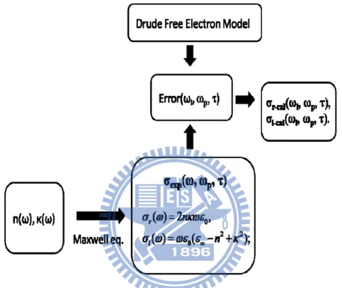
Figure 2-2-4 demonstrates the flow chart of the conductivity value extraction. It follows the steps as below. To get the experimental conductivity from the refractive index, we use the relations between the refractive index to the permittivity and the conductivity to the permittivity. The relations are derived from Maxwell equations. And then, we introduce Drude free electron model into the fitting process. With the experimental data and theoretical formula, we also define an error function to extract our parameters, ωp and τ.
2-3 Effective Medium Approximation:
If the body is neutral, the contribution to the average field may be expressed in terms of the sum of the fields of atomic dipoles. We define the average electric field E (r0) as the average field over the volume of the crystal cell that contains the lattice
point r0: 0 1 E(r )= ( ), c dV e r V
∫
⋅ --- (2-3-1)where e(r) is the microscopic electric field at the point r. Vc is the total volume of the
body. We called E the macroscopic electric field.
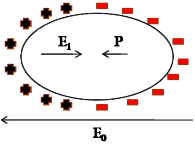
Depolarization Field: [19]
The geometry in many of our problems is such that the polarization is uniform within the body, and then the only contributions to the macroscopic field are from E0
and E1:
0 1;
E=E +E --- (2-3-2)
Here E0 is the applied field and E1 is the field due to the uniform polarization. The
field E1 is called the depolarization field, for within the body it tends to oppose the
27
Fig.2-3-1 Depolarization field E1 tends to oppose the applied field E0.
If Px, Py, Pz are the components of the polarization P referred to the principal axes
of an ellipsoid, then the components of the depolarization field are written (CGS) E1x = -NxPx; E1y = -NyPy; E1z = -NzPz; --- (2-3-3)
Nx, Ny, Nz are the depolarization factors and their values depend on the ratios of the principal axes of the ellipsoid.
Table 2-3-1 the depolarization factors for the body with different shapes
Shape Axis N(CGS) N(SI)
Sphere any 4π/3 1/3
Thin slab normal 4π 1
Thin slab in plane 0 0
Long circular cylinder longitudinal 0 0
Long circular cylinder transverse 2π 1/2
Local Electrical Field: [19]
The value of the local electric field that acts at the site of an atom is significantly different from the value of the macroscopic electric field. Now we consider the field
that acts on the atom at the center of the sphere. We write
Elocal = E0 + E1 + E2 + E3. --- (2-3-4)
Here
E0 = filed produced by fixed charges external to the body;
E1 = depolarization field, from a surface charge density n•P on the outer surface of
the specimen;
E2 = Lorentz cavity field: field from polarization charges on inside of a spherical
cavity cut out of the specimen with the reference atom as center.
E3 = field of atoms inside cavity.
Fig.2-3-2 Electric fields act on the center of the ellipsoid on the site of an atom.
The contribution E1 + E2 + E3 to the local field is the total field at one atom caused by
the dipole moments of all the other atoms in the specimen:
2 1 2 3 3( )5 E i i i i i, (CGS) i i p r r r p E E r − + + =
∑
i --- (2-3-5)The total local field at a cubic site is
0 1 4 4
E ;
3 3
29
macroscopic field E of equation 2-3-2 plus 4πP/3 from the polarization of the other atoms in the specimen where the Lorentz cavity is considering as the spherical shape.
2 2
0
4
( )(2 sin )( )( cos )(cos ) ;
3 E a a a d P P π π π θ θ θ θ − =
∫
⋅ ⋅ ⋅ = (CGS) --- (2-3-7)Fig.2-3-3 Calculation of the field in a spherical cavity in a uniformly polarized medium.
Clausius-Mossotti relation: [19]
The dielectric constant ε of an isotropic or cubic medium relative to vacuum is defined in terms of the macroscopic field E:
4 1 4 ; E P E π ε ≡ + = + πχ (CGS) --- (2-3-8)
The susceptibility in equation (2-3-7) is related to the dielectric constant by
P 1 = = . E 4 ε χ π − (CGS) --- (2-3-9)
The polarizability α of an atom is defined in terms of the local electric field at the atom:
p = α•Elocal , --- (2-3-10) where p is the dipole moment. The polarization of a
crystal may be expressed approximately as the product of the polarizabilities of the atoms times the local electric field:
( );
j j j j local
j j
P=
∑
N p =∑
N α E j (CGS) --- (2-3-11)where Nj is the concentration and αj is the polarizability of atoms j, and Elocal is the
local field at atom sites j. With Lorentz relation, then
4 ( )( ); 3 j j j P=
∑
N α E+ π P (CGS) --- (2-3-12) By solving equation 2-3-11, we find the susceptibilityP = = ; 4 E 1 3 j j j j j j N N α χ π α −
∑
∑
(CGS) --- (2-3-13)By definition ε = 1+4πχ in equation 2-3-7, we may rearrange 2-3-12 to obtain
1 4 ; 2 3 j j j N ε π α ε − = +
∑
(CGS) --- (2-3-14)This relation between the dielectric constant and the electric polarizability is called the Clausius-Mossotti relation.
Heterogeneous Dielectric and Effective-Midium Theory: [20]
31
Therefore the total polarization density from each quest phase contributes one such term to a sum of many is described in equation 2-3-11.
1 , K j j j P N p = =
∑
(CGS) --- (2-3-15)where Nj is the number density of the jth inclusion phase, and pj is the dipole moment
of a single inclusion of that phase. Here the number of different materials forming the mixture is K+1 because the environment material is not counted in the sum. With the Clausius-Mossotti relation, the final result for the effective permittivity is
1 4 1 ; 2 3 2 K K eff j j j j j j eff j N f ε π α ε ε ε − − = = +
∑
∑
+ (CGS) --- (2-3-16)where fj is the volume fraction of the inclusions of the jth phase in the mixture, αj is
the polarizability of such a sphere, and εj is its permittivity. As the result of the
definition for fj, =1; K j j f
∑
(2-3-17)Chapter 3 : ITO thin film characterization
3-1 Characters of Samples
ITO Thin Film (with O2 flux) shown in Fig. 3-1-1 to 3-1-3
Fig. 3-1-1 Film with thickness 961.6(nm)
The Fig.3-1-1 to 3-1-3 show the top views of our ITO film samples. The
magnification is ×50,000. The pictures with a scale 100nm make us find out the grain size of each sample. Therefore, we have the grain size, 30nm, 20nm, 10nm for the sample with thickness, 961.6nm, 483.0nm, 188.9nm, respectively.
33
Fig. 3-1-2 Film with thickness 483.0(nm)
Fig. 3-1-3 Film with thickness 188.9(nm)
In the SEM of ITO thin film, the grain size increasing is proportion to the film thickness. The value of the grain sizes are around several nm (30 nm to few nm). In the literature, the electron mean free path is below 5nm. [21] It means that the
dominate scattering mechanism of optical measurement is the same as the Hall measurement. In conclusion, we shall get a set of data by optical system being close to the hall measurement.
The cross diagram of ITO film with O2 flux has the geometry structure as below: in
Fig.3-1-4
Fig.3-1-4 The electron scattering at the grain boundary and the ionized impurity
[22]
There are many sources of electron scattering may influence the optical and electrical properties. The effects can separate between electron-defect scattering (i.e. grain boundaries and external surface, neutral and ionized point defects, dislocations, precipitations, and clusters), electron-lattice scattering (i.e. local deformation potentials), and electric-electron scattering. Original Drude model theory, without the damping term, is not sufficient for a quantitative model of the free electron properties in our sample. That is so because the damping term γ was introduced to our model.
35 Optical Spectroscopy of ITO Thin Film
The spectra of transmission type and reflection type spectrometer can distinguish the ITO film in different growth parameters, such as thickness [22], wt% of the target [23], and the flux of gas [24] et al.
In our case, all the conditions are fixed except the thickness of ITO films which are 961.6nm, 483.0nm, and 188.9nm. The thickness of ITO films are measured by “n & k-1500” at the center of our sample. The commercial “n & k 1500” are provided by NDL. The Fig.3-1-5 shows the plasma edge is increasing as the film thickness increasing. Around the plasma frequency, there is an important signature that is plasma edge where has the strong increase of absorption or reflection in the spectrum for transmission type or reflection type respectively. As the complex permittivity is describe by ε=εr+iεi, the plasma frequency Ωp is defined by εr(Ωp)=0.
We have to notice that Ωp is not equal to ωp, the Drude plasma frequency, mentioned
in chapter 2. They have the relationship
2 2 1 , p p ω ε∞ τ Ω = − --- (3-1-1) [22]
where τ is the scattering time and ε∞ is the relative permittivity at high frequency
range. In conclusion, the value of Ωp will smaller than the value ωp calculated from
Drude model.
Otherwise, we also can find out the energy band gap of the ITO is around 400nm ~ 3.1eV.
Fig.3-1-5 Spectra of JASCO: V-670 spectrometer (transmission type) for thin ITO films of the different thickness: 961.6nm, 483.0nm, and 188.9nm
In the Fig.3-1-5, we find out that as the thickness increasing the plasma edges are decreasing in the view of wavelength. The plasma edges are pointed by the arrow. [22]
Reflection Type Far Infrared Spectroscopy (R-FTIR)
The FTIR spectra were recorded using “Bomen da8.3” spectrometer by Instrument Center at National Tsing Hua University. The angle of incidence is 18˚ related to the sample normal. A ratio of the single beam spectra of ITO films to a single beam spectrum of a planar gold mirror was performed to obtain the reflectance spectra of ITO films with a 6mm hole to confine the detection range. The whole spectra cover from 0.6µm to 71.6µm (i.e. 15000cm-1 to 140cm-1).
37
Fig.3-1-6 FTIR of ITO film at short wavelength range with lower reflection part
Fig.3-1-7 FTIR of ITO film at long wavelength range with higher reflection part (The horizontal axis is in log scale.)
Similarly, we also can find out that the plasma edges are decreasing with the increasing of thickness (in the view of plasma wavelength). At the high frequency part, i.e. short wavelength part here, there are some vibrations which are the phenomena near the plasma edge. They also show strong thickness dependant that the thicker one has a high frequency variation in the part of short length edge, contrarily, for the thinner one. Both the transmission spectra and the reflection spectra have found the phenomena.
Hall Measurement
To act as a good electrode for solar cell, it should have both the good transparent property in solar range and low sheet resistivity (<10 Ω). [13] We have to deal our samples with optical measurement and electric measurement. The Hall measurement is used to get the electrical properties of the thin film samples. The model of the machine is “Ecopia HMS-3000”.
Table 3-1-1 ITO thin film electric properties measured by Hall measurement
By Hall (film on fused silica)
N (cm-3) µ (cm2V-1s-1) σ0 (Ω-1cm-1) ρ (Ω•cm) 188.9 (nm) -2.5×10²⁰ 38.4 1557 6×10⁻⁴ 483.0 (nm) -3.4×10²⁰ 38.0 2045 5×10⁻⁴ 961.6 (nm) -4.1×10²⁰ 34.3 2250 4×10⁻⁴
In the above table, carrier concentration is N, mobility is labeled by µ, DC conductivity is denoted by σ , and resistivity is given a symbol as ρ. With the Hall
39
measurement, we find out some characters of the thin film samples. The carrier concentrations and the DC conductivity increase as the thickness becoming larger. The Hall mobility of the thin films is close to each other.
Table 3-1-2 The sheet resistivity of Hall measurement compared with 4-point probe measurement
Hall v.s. 4-point probe (film on fused silica)
Sheet R (Ω/□)-Hall Sheet R (Ω/□)-NDL
188.9 (nm) 34.03 36.05
483.0 (nm) 10.1 10.48
961.6 (nm) 4.62 4.62
The sheet resistivity of Hall is closely to the 4-point probe method for the ITO film at each thickness. It is a recheck. With the growth of the sample thickness, the sheet resistivity becomes smaller. ITO thin film with thickness, 961.6nm, has the lowest sheet resistivity bellowing 10Ω/□. It means that it turns to be the crystalline structure. It will be proved in the spectrum of X-ray diffraction.
3-2 Reflection Type FTIR using Drude Model fitting
ITO thin films have been widely studied in the optoelectronic industry because they combine unique transparent and conducting properties. The optical research of ITO in FTIR is also well studied with Drude free electron model by different assumption details. There are some examples:
In earlier 1980s, they dealt the problem with simple optical reflection assumption, A=1-R-T, to extract ε(ω). A is the power absorption, R is the power reflection, and T
is the power transmission. [25] The group, D. Mergel et al, did it also with simple optical assumption. Otherwise, they modified the dielectric model to have more parameters as variables to well fit the curve of the ITO film FTIR spectrum. [26] FTIR spectra of ITO film with different angle incidence were fitted with two-phase Fresnel equations and three-phase Fresnel equations for Reflectance by the group, H. Scott et al. [27] Therefore, using the Drude model to extract the information of ITO thin film is a well known method.
Fitting Model and Reflectance FTIR Spectroscopy
The spectra of ITO film determined by NDL using a Bruker IFS66v/S spectrometer are used to do the following analysis. The spectra were obtained with incident angle 11˚ and a hole 7mm on the sample mount. Gold mirror was used as reference spectrum in the measurement. With a spectrum range, 400 cm-1 to 7500 cm-1, reflection type FTIR of ITO films were recorded.
5 10 15 20 25 0.0 0.4 0.8 R 1.33~25um film 961.6nm film 483.0nm film 188.9nm
41
The peaks around 25μm and 10μm are the phonon absorption. [21] With the thickness growth up, the reflection peaks will become smaller or undetermined. It could be modeling by introducing the damped Lorentz oscillators in infra-red range. But in our modeling, we neglect the phonon part to do the fitting process.
How to model the curvature of ITO FTIR spectra? The Drude free electron model is used to fit ITO film spectra.
2 2 1 ( )= p ; i ε ω ε ω ω ω τ ∞− +
where ε∞ is the high frequency dielectric constant, ωp is the Drude plasma frequency,
ω is the frequency, and τ is the electron scattering time.
The plasma frequency is defined by ωp2=Ne2/mε0, where N is the carrier concentration.
With the three-phase Fresnel equations for reflectance, we have
2 12 23 2 12 23 , 2 N cos . 1 i p p p i p p r r e d r r r e δ δ δ π λ + = = Θ
+ The subscript “p” means that in p – polarization and the basic diagram of the sample is “1/2/3 to air/ITO/glass (FS)”. δ is the path difference and N is the complex refraction index of ITO film.
With the two assumptions above, we can get the theoretical expression of reflection for ITO film. The diagram of flow chart as shown in next page: Fig.3-2-2
Fig.3-2-2 It shows how to get the plasma frequency, and carrier scattering time from FTIR spectra.
In the Fig.3-2-2, it is the flow chart of FTIR reflectance spectrum fitting. Bruker IFS66v/S spectrometer was used to get the spectrum with the x-axis is the wave number. Then we have to transverse the data to angular frequency dependent. With the theoretical formula and the experimental results, we can define a error function in our fitting process to extract the parameters, ωp and τ, the plasma frequency and the
carrier scattering time.
43
Fig.3-2-3 Fitting curve of ITO film with thickness 188.9nm
Table3-2-1 Fixed parameters
ε∞ nFS
4 1.4
Table3-2-2 Fitting parameters of ITO film 188.9nm
ωp(rad.THz) τ(fs) µ(cm 2
/Vs) N(cm-3)
Fig.3-2-4 Fitting curve of ITO film with thickness 483.0nm
Table3-2-1 Fixed parameters
ε∞ nFS
4 1.4
Table3-2-3 Fitting parameters of ITO film 188.9nm
ωp(rad.THz) τ(fs) µ(cm 2
/Vs) N(cm-3)
45
Fig.3-2-5 Fitting curve of ITO film with thickness 961.6nm Table3-2-1 Fixed parameters
ε∞ nFS
4 1.4
Table3-2-4 Fitting parameters of ITO film 961.6nm
ωp(rad.THz) τ(fs) µ(cm 2
/Vs) N(cm-3)
In the Table3-2-1, ε∞ is the high frequency dielectric constant. nFS is the refraction
index of fused silica in this spectral range.
In the Table3-2-2, 3-2-3, and 3-2-4, the mobility is calculated from µ=eτ/m*, where m* = 0.35 me [21] is the effective mass of ITO. N is the carrier concentration
that satisfied N= ωp2m*ε0/e2, where e is the electron charge with unit coulomb.
In Fig.3-2-3 to 3-2-5, we find out that there are two resonate peak in the period from 30 ~ 37.5THz (i.e. 8µm to 10µm). It is the signature of our ITO film [21], but we did the fitting without including these futures. In order to compare the reflection spectra with Drude formula, we neglected the phenomenon. And the fitting range is from 12 THz to 225 THz (i.e. 400 cm-1 to 7500 cm-1).
In summary, we get the results similar to the Hall measurement by Drude free electron model fitting. And Drude model works very well for the whole spectrum except the unknown resonance. In conclusions, the plasma frequency is increasing as the thickness increasing in the view of frequency (the unit of x-axis is Hz). The carrier concentration has the same behavior. And the mobility is in the range of Hall measurement. As result, the carrier scattering time is comparable to the literature [27].
47
Table3-2-5 Fitting parameters of ITO film, 961.6nm, 483.0nm, and 188.9nm compare with the Hall measurement.
FTIR ωp(THz) τ(fs) µ (cm2/Vs) N (cm-3) σ0 (Ω-1cm-1) Rs (Ω/□) Film: 188.9(nm) 1600 6.8 34.2 2.8×10 20 1532 34.6 Film: 483.0(nm) 1860 6.7 33.7 3.8×10²⁰ 2049 10.1 Film: 961.6(nm) 1950 6.4 32.2 4.2×10²⁰ 2164 4.8 Hall Film: 188.9(nm) 38.4 -2.5×10²⁰ 1557 34.03 Film: 483.0(nm) 38.0 -3.4×10 20 2045 10.1 Film: 961.6(nm) 34.3 -4.1×10 20 2250 4.62
In table 3-2-5, we also can find out that the DC conductivity and the sheet resistivity are comparable to the electrical measurement.
3-3 THz Time Domain Spectroscopy
System Set Up (Transmission Type)
Fig.3-3-1 Antenna THz time domain spectroscopy system
It is an optical pump probe system with the pulse duration, 50fs, the center wavelength, 800nm, and the repetition rate, 80MHz. The emitter and the receiver are composed by GaAs. And the THz pulse width was 1ps with a frequency domain spectrum 0.15 ~ 3THz. We purged the system with the nitrogen when we were measuring.
49
Data Analysis
Fig.3-3-2 THz waveform transmits through ITO film with thickness 188.9nm.
The lower one is the signal for ITO film, and the higher one is the reference for the fused silica. In the Fig.3-3-2, we find out that the peak positions are at the same delay time. That is because the sample is very thin. Therefore, in the time domain waveform, we cannot distinguish the reference peak position and the signal peak position with the delay resolution, 10μm. Note here: the delay stage of the system steps 1μm. The corresponded delay time to the time domain spectroscopy is 2μm.
Fig.3-3-3 THz frequency domain spectra of TO film with thickness 188.9nm
The lower one is the signal for ITO film, and the higher one is the reference for the fused silica. With the frequency domain spectroscopy, we could derive out the refractive index. It is because the absorption of the ITO thin film is very obvious. Note here: with the nitrogen purge, we have the frequency domain spectrum above. There are almost no water absorption peaks in the spectrum. It will make our analysis to be more convinced.
51
Fig.3-3-4 The refraction index of TO film with thickness 188.9nm.
κ value is larger than n value at the high frequency part, and they are going to become close at the low frequency part.
Fig.3-3-5 σ(ω) of TO film with thickness 188.9nm
It shows the Drude model like behavior. Therefore we fit the data with Drude free electron model.
Fig.3-3-6 THz waveform transmits through ITO film with thickness 483.0nm.
The lower one is the signal for ITO film, and the higher one is the reference for the fused silica. In the Fig.3-3-6, we can also find out that the peak positions are at the same delay time. That is because the sample too thin to distinguish the reference peak position and the signal peak position with the delay resolution, 10μm.
53
Fig.3-3-7 THz frequency domain spectra of TO film with thickness 483.0nm
The lower one is the signal for ITO film, and the higher one is the reference for the fused silica. With the frequency domain spectroscopy, we could derive out the refractive index. It is because the absorption of the ITO thin film is very obvious. Note here: with the nitrogen purge, we have the frequency domain spectrum above. There are almost no water absorption peaks in the spectrum. It will make our analysis to be more convinced.
Fig.3-3-8 The refraction index of TO film with thickness 483.0nm
κ value is larger than n value at the high frequency part, and they are going to become close at the low frequency part.
Fig.3-3-9 σ(ω) of TO film with thickness 483.0nm
55
Fig.3-3-10 THz waveform transmits through ITO film with thickness 961.6nm.
The lower one is the signal for ITO film, and the higher one is the reference for the fused silica. In the Fig.3-3-10, the peak positions of the reference and the signal are separated. It means that with the time resolution fixed at 10μm. We could distinguish the peak position of the reference and the signal as the thickness of ITO thin film up to 1μm. In the figure, we also can find out that the difference of them is only one step.
Fig.3-3-11 THz frequency domain spectra of TO film with thickness 961.6nm
The lower one is the signal for ITO film, and the higher one is the reference for the fused silica. With the frequency domain spectroscopy, we could derive out the refractive index. It is because the absorption of the ITO thin film is very obvious. Note here: with the nitrogen purge, we have the frequency domain spectrum above. There are almost no water absorption peaks in the spectrum. It will make our analysis to be more convinced. But in the high frequency range, the signal and noise ratio is smaller. Therefore, the analysis is limited by the SN ratio of the spectrum.
57
Fig.3-3-12 The refraction index of TO film with thickness 961.6nm
κ value is larger than n value at the high frequency part, and they are going to become close at the low frequency part.
Fig.3-3-13 σ(ω) of TO film with thickness 961.6nm
It shows the Drude model like behavior. Therefore we fit the data with Drude free electron model.
Fig.3-3-14 Compared the frequency domain spectra of the ITO thin films
Fig.3-3-15 Compared the refractive index of the ITO thin films
Fig.3-3-16 Compared the conductivity of the ITO thin films
From the left to the right, they are following the rule, 188.9nm, 483.0nm, and 961.6nm, respectively.
59
In the Fig.3-3-14, we find out the amplitude of the frequency domain spectra becoming lower as the thickness growing up. And it will cause the SN ratio to be bad. Therefore, the usage spectrum will become smaller with the sample thickness increasing.
In the Fig.3-3-15, we find that as the thickness increasing the refractive index is also increasing. But the value of the real part refractive index cannot be told from the time domain spectroscopy. It is because the signal is mixing so much frequency and it is the result of multibeam interference. We cannot tell the difference between the reference and the signal for the thin sample with the long time delay. And in the literature [28], the refractive index of ITO thin film at THz range is similar to our results.
In the Fig.3-3-16, the real part of the conductivity has become larger as the thickness of sample increasing. And we also find that as the SN ratio becoming badly, we cannot find a suitable result. Therefore, we introduce the parameters of FTIR into the THz-TDS analysis to recheck the data.
The plasma frequency of ITO film is far away from our light source spectrum. If there is a little vibration in σ(ω), it will mislead the fitting parameters that cannot extract the exact optical and electrical constants. Therefore, we introduce the plasma frequency calculated from FTIR into our conductivity fitting to recheck the optical measurement properties.