矽智產設計的功率估測方法之研究
120
0
0
全文
(2) 矽智產設計的功率估測方法之研究 學生:許智揚. 指導教授:周景揚 博士 劉建男 博士. 國立交通大學 電子工程學系. 摘. 電子研究所. 要. 在這篇論文中,我們針對組合邏輯電路的矽智產單元提出了一系列的功率消耗估測 方法及功率消耗模型。因為矽智產供應商為了保護他們的設計概念可能只提供矽智產使 用者有限的設計資訊,因此我們對應電晶體層級、閘層級以及功能層級之電路設計資訊 提出不同的功率消耗估測方法及功率消耗模型。 針對提供電晶體層級設計資訊的複雜數位電路,矽智產使用者可以採用電晶體層級 的模擬估測功率消耗,而圖樣壓縮法已經被採用來加速電晶體層級的功率消耗之估測。 在此,我們提出單一序列取樣法減少了傳統圖樣壓縮方法採用的隨機取樣法中無用的圖 樣轉換,達到改進傳統圖樣壓縮的效果。並更進一步提出多序列取樣法改善單一序列取 樣法過度取樣的缺點。 針對只提供閘層級設計資訊的電路,我們提出一個較小的功率消耗模型。這個功率 消耗模型只須要使用輸入信號轉換時電路的零延遲充電及放電電容值當索引就可對照. i.
(3) 出實際功率消耗的估測值。因此矽智產使用者只要使用閘層級模擬時得到的零延遲充電 及放電電容值就可以查表得到實際功率消耗的估測值。在這個方法中我們採用了分群的 方法減小對照表,並利用蒙地卡羅模擬法縮短了建立對照表的時間。根據實驗結果顯 示,這個功率模型針對不同的輸入信號序列依然具有高度的準確性。 如果矽智產供應商只願意提供功能層級的設計資訊,則矽智產使用者只能獲得電路 輸入及輸出的對應關係。我們針對這種應用提出一個採用類神經網路建立的全新功率消 耗模型。假如矽智產供應商提供這樣的功率消耗模型,則矽智產使用者只須要使用功能 層級模擬得到的電路輸入及輸出資訊就可以推估電路之功率消耗值。如同實驗結果所顯 示,這個功率消耗模型同時具有低複雜度及高準確度的優點。. ii.
(4) On Power Estimation Methods for Silicon Intellectual Properties Student: Chih-Yang Hsu. Advisor: Dr. Jing-Yang Jou Dr. Chien-Nan Liu. Department of Electronics Engineering Institute of Electronics National Chiao Tung University. Abstract In this dissertation, we develop several power estimation and power modeling methods for combinational IPs. Because IP vendors may release only limited design information to protect their knowledge, we propose corresponding methods for the designs with only transistor-level, gate-level and function-level design information. For complex digital circuits with transistor-level design information, users can estimation the power consumption of designs using transistor-level simulation. In order to reduce the simulation time on transistor-level simulation, we propose a single-sequence sampling approach to improve the performance of vector compaction techniques by reducing the useless transitions in random sampling techniques. A multi-sequence sampling approach is also proposed to improve the over sampling problem in the single-sequence sampling approach. iii.
(5) For the designs with only gate-level design information, we propose a smaller power model approach that only needs a 1-diemension lookup table for each design to map the zero-delay charging and discharging capacitance (CDC) during an input pattern transition to an estimative value of real power consumption. Therefore, IP users can estimate the power consumption according to the CDC values obtained from gate-level simulation. The dynamic grouping method is applied to reduce the size of lookup tables for circuits and Monte-Carlo simulation strategy is applied to reduce the characterization time. The experimental results show that our power model still has high accuracy for different input sequences. If IP vendors only provide the function-level design information, we propose a novel power model based on neural network that only requires the input and output information of each IP. If IP vendors provide such a power model, IP users can estimation the power consumption of IPs with only input and output information under a function-level simulation. As shown in the experimental results, our power model can have much smaller size with better accuracy.. iv.
(6) 誌謝 首先我要誠摯地感謝周景揚教授以及劉建男教授。沒有他們的鼓勵、督促及耐心的 指導,我不可能完成這篇論文。周老師不只在研究上給予我許多的指導,他也在日常的 學習及生活態度上給予我最好的典範。劉教授對於我研究上的指導不遺餘力,對於這篇 論文最後的撰寫也提供了他寶貴的意見。 我也要感謝我的另外一位指導教授沈文仁博士(1952~2002), 他在 1995 年到 2002 年期間一直擔任我的指導教授,雖然他無法親眼看到我的畢業論文,但是在我完成這篇 論文的同時,我也希望他能同感榮耀。 我也要感謝我的父母親及家人,沒有他們的支持,我不可能走過這條漫長的道路。 由於父母親全力的支持,我才能在攻讀學位期間沒有後顧之憂。由於兄姊對家中的照 顧,我才能在沒有家庭經濟壓力的情況下完成這項工作。我也要感謝我的女朋友馮麗 卿,在我攻讀博士學位期間漫長的等待與支持。 我同時也感謝實驗室許多學長姊及學弟妹們的幫助。感謝許文俊學長、林景源學 長、黃俊達學長、黃恆亮學長對於我研究及實驗室工作大力的幫忙,感謝中央大學電機 系薛文燦學弟在類神經功率模型上長期的投入並忍受長時間的奔波,更感謝許多曾經共 同與我在同一實驗室度過無數歲月的學弟妹們,他們都是我完成這篇論文的支持者。 謹將這篇論文獻給所有曾經對我的博士論文有過幫助或關心的人。. v.
(7) Contents I. 摘要 Abstract. III. 誌謝. V. Contents. VI. List of Tables. IX. List of Figures. X. Chapter 1 Introduction. 1. 1.1 Power Consumption…………………………………………………………. 3 1.2 Power Estimation……………………………………………………………. 6 1.2.1 Simulation-Based Methods………………………………………….. 7 1.2.2 Statistics-Based Methods…………………………………………… 11 1.3 Approaches for Different Design Information……………………………… 14 1.3.1 Power Estimation at Transistor Level………………………………. 14 1.3.2 Power Estimation at Gate Level…………………………………….. 15 1.3.3 Power Estimation at Behavior Level………………………………... 16 1.4 Organization………………………………………………………………… 18. Chapter 2 Improved Vector Compaction Methods. 19. 2.1 Vector Compaction Techniques…………………………………………….. 19 2.2 Useless Transitions…………………………………………………………. 22 2.3 Selection of Power Characteristics…………………………………………. 24. vi.
(8) 2.4 Grouping of Pattern Pairs………………………………………………….. 29 2.5 Consecutive Sampling Techniques…………………………………………. 34 2.5.1 Single-Sequence Approach………………………………………… 34 2.5.2 Multiple-Sequence Approach………………………………………. 39 2.6 Average Power Calculation…………………………………………………. 44 2.7 Experimental Results……………………………………………………….. 45 2.8 Summary……………………………………………………………………. 48. Chapter 3 Gate-Level Power Model with 1-D LUT. 50. 3.1 Power Model with Lookup Table…………………………………………... 50 3.2 Proposed Power Modeling Methodology………………………………….. 53 3.3 Dynamic Grouping…………………………………………………………. 54 3.4 Power Characterization…………………………………………………….. 58 3.5 Power Estimation with the Power Model…………………………………... 62 3.6 Experimental Results……………………………………………………….. 64 3.7 Summary……………………………………………………………………. 65. Chapter 4 High-Level Power Model with Neural Network. 67. 4.1 High-Level Power Modeling………………………………………………. 67 4.2 Background about Neural Networks…….………………………………… 71 4.2.1 Feedforward Neural Networks…………………………………….. 71 4.2.2 Training Process……………………………………………………. 73 4.2.3 Evaluating the Accuracy of a Trained Neural Network……………. 76 4.3 Power Model Construction with Neural Networks………………………… 77 vii.
(9) 4.3.1 Building Neural Network…………………………………………... 79 4.3.1.A Input Data Type and Transfer Function……………………. 79 4.3.1.B Number of Hidden Neurons……………………………….. 84 4.3.2 Design of Training Sets…………………………………………….. 86 4.4 Experimental Results………………………………………………………. 88 4.5 Summary…………………………………………………………………… 93. Chapter 5 Conclusions and Future Works. 94. Reference. 97. viii.
(10) List of Tables Table 2-1. Average normalized errors for three power characteristics……………… 29 Table 2-2. The relationship between compaction ratio, variance limitation and estimation error……………………………………………………………………... 33 Table 2-3. A comparison of random, single-sequence and multi-sequence techniques ……………………………………………………………………… 46 Table 2-4. Consecutive sampling techniques for LFSR input sequences…………… 47 Table 3-1. The distribution of the variance in the groups…………………………… 62 Table 3-2. The experimental results………………………………………………… 65 Table 4-1. Comparison of input data types vs. transfer functions………………….. 84 Table 4-2. The effects of the number of hidden neurons…….……………………... 85 Table 4-3. The effects of the size of training set…………………………………….. 87 Table 4-4. The comparison between traditional 3D LUT power model and our neural power model……………………………………………………………. 90. ix.
(11) List of Figures Figure 1-1. Dynamic transition current………………………………………………. 4 Figure 1-2. Short-circuit current……………………………………………………… 5 Figure 1-3. Leakage current………………………………………………………….. 5 Figure 1-4. Static current……………………………………………………………… 6 Figure 2-1. Random sampling with useless transition………………………………. 22 Figure 2-2. Consecutive sampling…………………………………………………… 23 Figure 2-3(a). The result of single-sequence approach……………………………… 24 Figure 2-3(b). The result of multi-sequence approach……………………………… 24 Figure 2-4. The effects of grouping…………………………………………………. 31 Figure 2-5. An example of grouping process (a). CDC distribution…………………………………………………………… 31 (b). Sorting and grouping……………………………………………………….. 31 Figure 2-6. The pseudo code of the grouping algorithm……………………………. 34 Figure 2-7. The pseudo code of the single-sequence algorithm…………………….. 37 Figure 2-8. An example of the shortest subsequence searching…………………….. 39 Figure 2-9. Transforming a X3C problem into a multi-sequence problem…………. 40 Figure 2-10. The pseudo code of the multi-sequence algorithm……………………. 42 Figure 2-11. An example of the multi-sequence algorithm……………………….… 43 Figure 3-1. The block diagram for building the power model………………………. 54 Figure 3-2(a). The dynamic grouping process after the first iteration………………. 56 Figure 3-2(b). The dynamic grouping process after the second iteration…………… 56 x.
(12) Figure 3-3. The pseudo code of dynamic grouping process………………………… 58 Figure 3-4. An illustration of the power characterization…………………………… 59 Figure 3-5. Block diagram of average power calculation…………………………… 63 Figure 4-1. Irregular power distribution and piece-wise approximation……………. 68 Figure 4-2. An artificial neuron……………………………………………………… 72 Figure 4-3. A fully connected 3-layer feedforward neural network…………………. 73 Figure 4-4. The workflow of building a neural power model……………………….. 78 Figure 4-5(a). An example of the bit-level statistics characterization………………. 81 Figure 4-5(b). Input data format with bit-level statistics……………………………. 81 Figure 4-5(c). An example of the word-level statistics characterization……………. 81 Figure 4-5(d). Input data format with word-level statistics…………………………. 81 Figure 4-6. Scatter plot of neural power model estimation versus PowerMill simulation in ISCAS’85 benchmarks……………………………………………. 91 Figure 4-7. Scatter plot of 3D-LUT estimation versus PowerMill simulation in ISCAS’85 benchmarks……………………………………………….. 91. xi.
(13) Chapter 1 Introduction With the advance of semiconductor technology, the size of devices and the minimal width of metal lines are decreasing rapidly. Therefore, IC designers could integrate many functions, even a whole system, into a single chip. In fact, System-on-a-chip (SoC) is a trend of system integration in recent years. Meanwhile, the operating frequency of designs also rapidly grows up when the semiconductor technology getting advances. Unfortunately, after more devices are integrated into a chip and the operation frequency is increased, the power consumption of a chip is also increasing rapidly. For SoC designs, most design teams will not design all circuit blocks in the system by themselves. Instead, they integrate many well-designed circuit blocks called intellectual properties (IPs) and some self-designed circuit blocks to build up the complex system in a short time. While designing such complex systems, power consumption is also a very important design issue because of the increasing requirement of portable devices. Traditionally, power estimation is often performed at transistor-level by SPICE-liked simulation. However, this approach is unpractical for SoC designs because the transistor-level description of the whole designs is often too large to be simulated and the IP venders may not provide such low-level description for an IP to protect their knowledge. For this application, the power estimation method should consider the design information of IPs that IP vendors want to explore to IP users. For example, if the 1.
(14) transistor-level descriptions of IPs are provided to IP users, IP users can estimate the power consumption with a transistor-level simulation. The only problem is the efficiency of the estimation. If the gate-level descriptions of IPs are the only design information provided to IP users, IP vendors should provide some information such that IP users can estimate the power consumption of IPs from some power characteristics, which can be calculated from a gate-level simulation. If IP vendors only want to provide the design information for function checking such that IP users can only get the primary input and primary output signals, IP vendors should provide a high-level power model in which IP users can estimate the power consumption of their designs using only the primary input and output information. In this dissertation, we develop several power estimation and power modeling methods according to the design information that IP vendors will provide to IP users. We divide the design information into three levels. The first level is transistor-level information. The second level is gate-level information. The third level is behavior-level information. For those three levels, we develop three corresponding power estimation methods. For the complex digital circuits with transistor-level and gate-level design information, we propose two consecutive sampling techniques to improve the losing of performance in those pattern compaction methods with random sampling techniques. IP users can apply our proposed pattern compaction method to reduce the simulation time on a transistor-level simulator with reasonable accuracy. For the IPs with only gate-level design information, we propose a power model in which a lookup table is built for each IP that maps the zero-delay charging and discharging capacitance during a input pattern transition to an estimative value of real power consumption. 2.
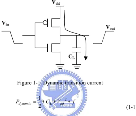
(15) Therefore, IP users can estimate the power consumption according to the zero-delay charging and discharging capacitance from gate-level simulation. The grouping method is applied to reduce the size of lookup tables for circuits and Monte-Carlo simulation strategy is applied to reduce the characterization time. If IP vendors only provide the behavior-level design information, we propose a power model based on neural network in which only the input and output information of an IP is required to obtain the estimated power. Therefore, IP users can estimation power consumption of IPs with the input and output information obtained from a function-level simulation. Compared to the state-of-the-art 4-D lookup table, our approach requires much less memory but still has competitive accuracy. Before discussing how the power estimation can be done, we would like to introduce the power consumption of CMOS digital circuits and the incurred problems by the increasing power consumption.. 1.1 Power Consumption The power consumption of a CMOS digital circuit comes from four major types of current, which are dynamic transition current, short-circuit current, leakage current and static current. We will briefly explain the four kinds of current resources in the following descriptions. The dynamic transition current is resulted from the charge and discharge of the node capacitance. In Figure 1-1, an inverter circuit is used to explain the dynamic transition current. The power consumption of dynamic transition current on output node is often formulated as 3.
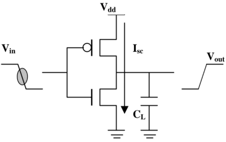
(16) Equation (1-1), when logical value of output node is changed from 0 to 1. The same power consumption will be consumed during the logical value of output node is discharged from 1 to 0. In Equation (1-1), f is the frequency of signal transition on output node. In general, the dynamic power is the largest part of the total power consumption in a circuit. Vdd. Vin. Vout. CL. Figure 1-1. Dynamic transition current. Pdynamic =. 1 ∗ C L ∗ Vdd 2 ∗ f 2. (1-1). The short-circuit current is the current from Vdd to ground at the period that both PMOS and NMOS transistors turn on together during the input signal transitions. As illustrated in Figure 1-2, both PMOS and NMOS transistors are turned on together during the gray circle period of input signal Vin, and the short-circuit current occurs at that moment. The power consumption of short-circuit current can be formulated as Equation (1-2), in which Isc is the mean value of short-circuit current. The short-circuit current could be minimized by matching the rise/fall times of the input and output signals.. 4.
(17) Vdd. Vin. Isc. Vout. CL. Figure 1-2. Short-circuit current Pshort −circuit = I sc ∗ Vdd. (1-2). The leakage current is the current from Vdd to ground even when the PMOS path or the NMOS path is “OFF”. It is often consisted of the leakage current in the reverse biased P-N junction diode between n-wall and substrate and the sub-threshold current from sub-threshold conduction, as illustrated in Figure 1-3. The leakage power consumption can be formulated as Equation (1-3), in which Ileakage is the mean value of leakage current. Vdd. Vin. Ileakage. Sub-threshold Current. Vout. Drain Junction Leakage. Figure 1-3. Leakage current. Pleakage = I leakage ∗ Vdd. 5. (1-3).
(18) Another power source is the static current that occurs in some special logic family, such as the pseudo-NMOS logic family. In such kind of circuits, there is always a constant current from the Vdd to ground, as illustrated in Figure 1-4. The static power consumption can be formulated as Equation (1-4), in which Istatic is the mean value of static current. Vdd. Istatic. Vout. Vin=”High”. Figure 1-4. Static current. Pstatic = I static ∗ Vdd. (1-4). 1.2 Power Estimation The demand of portable devices and the functions integrated in those devices are both dramatically. increasing. day-by-day.. However,. those. portable. devices. are. often. battery-operated. Increased power consumption means reduced operating time. In addition, increased power consumption also increases the heat generation of chip. In order to remove the extra heat to protect inner circuits, special packaging, cooling and fans are required, which lead to higher cost. Furthermore, larger power consumption may increase the current density of the metal lines in a chip and the temperature of the chip such that several silicon failures, such as electromigration, junction fatigue, and gate dielectric breakdown [1,2], may 6.
(19) become more likely to happen. Therefore, the power consumption has also become one of the most important design constraints beside timing and area constraints in present designs. At the design stage, various low-power design techniques have been proposed at each different level of abstraction, such as system-level, architecture-level, register-transfer level, gate-level and transistor-level. Many surveys on those low-power design techniques could be found in [3~9]. However, before using those low-power design techniques, we have to know the power consumption of current designs. Based on the power estimation results, designers can understand whether any low-power techniques are required and where to apply those low-power techniques to reduce the power consumption of the circuit. In the literature, many power estimation techniques have been proposed. They can be roughly categorized as simulation-based methods and statistics-based methods, according to the used information while calculating the final power consumption of circuits. In this section, we will introduce those two techniques briefly. Earlier surveys for those power estimation techniques could be found in [9~12].. 1.2.1 Simulation-Based Methods Basically, simulation-based techniques will use simulators to perform power estimation. In those techniques, the most straightforward method of power estimation is to perform circuit simulation to obtain the current information and the resulted power consumption. SPICE is the transistor-level simulator that can provide the most accurate estimation to date. It solves the combination of KVL and KCL equations for the voltages of all nodes and the currents of some certain branches. Although it can provide more accurate results, it will suffer. 7.
(20) from severe memory and execution time constrains, especially for large VLSI circuits. In order to alleviate the memory and speed issues for power estimation, PowerMill [13,14], which is a transistor-level power simulator for CMOS and BiCMOS VLSI designs, applies an event-driven simulation algorithm to increase the speed by two or three orders of magnitude over SPICE. Moreover, it uses a nonlinear device model instead of resistor model to model the transistors such that it can maintain the SPICE accuracy while increasing the simulation speed. Estimating power consumption at switch level is another idea to have faster simulation speed, such as the well-known tool IRSIM [15]. Because it only counts the switching power dissipation, which is the transition counts of the circuit nodes weighted by physical node capacitances, the simulation speed is often much faster than that of a transistor-level simulation. However, the estimation results of such tools may not as accurate as those of transistor-level tools. If the simulation can be done at higher level of abstraction, such as gate-level, the simulation speed could be improved much more. Therefore, many gate-level simulation techniques are proposed to estimate the power consumption of cell-based designs based on the characterization results of library cells. In general, the characterization results include the power model and delay model of basic cells. The power model could be a lookup table or an equation such that the power consumption of a circuit could be calculated by summarizing the power consumption of each basic gate in the circuit. In [16~20], the characterization flow for the cells in a cell library is proposed and the power consumption of circuits is calculated using a gate-level simulator according to the characterization result. The differences between those approaches are the accuracy of the delay model and power model of basic cells, or the 8.
(21) accuracy on estimating glitch power. For example, in [18], the authors include a glitch filter to reduce the over estimation on glitch power. In [21, 22], the basic unit of power characterization is extended to complex logic blocks or some functional units on datapath such that their performance is much more improved. Although the gate-level simulation speed is much faster, most of those techniques have to make a tradeoff between the accuracy and the storage complexity. Besides increasing the simulation speed, another approach is to reduce the number of input patterns for power estimation such that the transistor-level simulation time can also be reduced. Such kind of power estimation methods can be roughly divided into two directions: regeneration and sampling. Regeneration approach [23~30] is to generate a new input sequence that is shorter than the original input sequence but has the similar average power as that of the original one. Some characteristics of the original sequence, such as the pattern transition probabilities [23], the pattern transition probabilities of those input pins with higher power sensitivity values and the average transition probability of rest input pins [24], and the ratio of state transition number of each state [25,26], are preserved during the generation process. In order to reduce the complexity of the generation process, some approaches [27,28] only preserve the input characteristics between clustered inputs. There are also some methods trying to preserve the toggling behavior of the internal nodes [29~30] between the original input sequence and the regenerated input sequence. Instead of generating new input patterns, the sampling approach chooses some input patterns from the original sequence to estimate the average power. The Monte Carlo approach for power estimation is proposed in [31,32]. These methods estimate the average power by 9.
(22) sampling some input vectors with certain length l from the original sequence and feeding them into the simulator to derive a sample value of the average power. The average power consumption can be estimated with the average of several sample values. From Central Limit. Theorem [33~36], the sample values can be assumed as a normal distribution when l approaches infinity. The probability that the estimated mean value is within a certain error range of the real mean value can also be derived under this assumption. In [31], only combinational circuits are considered and sequential circuits are considered in [32]. Sampling techniques can be further optimized through stratification of the population. Proper stratification of the population can reduce the sample variance such that the number of sampled input vectors can be further reduced. In order to stratify the input vectors, various indicator functions are proposed to provide a rough estimation of the power consumption of each input vector. According to the results of indicator functions, we can put the input vectors with similar power consumption into the same group and sample only a few patterns from each group. Therefore, the key point of this approach is to choose a good indicator function. In [37], the power characteristic is chosen as the zero-delay switching activity multiplied by the loading capacitance of each node. Those power characteristics of input pattern pairs are used to divide input pattern pairs into clusters such that the Monte Carlo simulation [36] could randomly sample the same number of pattern pairs from each cluster. This stratified random sampling could improve the convergence speed of the Monte Carlo simulation. In [38], the transition numbers of primary inputs, primary outputs, latches and selective internal nodes are used as the indicator function. Only when the indicator function has enough value changes, this input pattern pair will be used in the transistor-level simulation to 10.
(23) plot the power waveform of the input sequence. In [39], the zero delay switching conditions at gate level is used as the indicator function and the modules in the design is also clustered to improved the performance again. In [40], a cycle-based characteristic, the real-delay charging and discharging capacitance, is used as the indicator. They divide all pattern pairs into groups and select only one pattern pair from each group. This approach may not suitable for the designs with very deep logic level because the small delay time error will cause large power variance due to glitch.. 1.2.2 Statistics-Based Methods Statistics-based techniques can be categorized into several different levels. Some of them use the entropy [41~45] for high-level power estimation and modeling because the required information in this approach is independent of the wire loading, transistor sizes, gate types or even circuit structure. Using the analytical results between entropy and real power, we can obtain rough power estimation using only high-level or behavior-level information. Since the simulation at such a high level can be completed very fast, we can have a quick indicator about power consumption in early design stages. However, the power estimation results of this approach will not be very accurate due to the lack of real circuit information. In [46], the entropy is also used to estimate gate counts or area of Boolean functions, and the power consumption of the design could be calculated from switching activity and loading capacitance of each node in the circuit. The basic entropy calculation of logic circuit could refer to [47]. If gate-level design information is available, many researches will calculate the signal. 11.
(24) transition density [48] or switching activity of each node in the circuit to estimate the power consumption. The estimation results can be more accurate because the power consumption of CMOS digital circuits are dominated by the currents that charge and discharge load capacitances and the short circuit currents. In early researches, gate-level power estimation focuses on combination circuits [49~51]. They assume that the primary inputs are spatially and temporally independent and the propagation delay of each gate is zero. In order to improve the accuracy of power estimation results, the spatial and temporal correlations are included for switching activity estimation in [52~54]. However, the computational complexity to consider spatial correlation may become too high to be adopted. In [55~59], they start to extend the gate-level power estimation to sequential circuits. In, [56, 57], the BDD (Binary Decision Diagram) is used for the switching activity estimation. In [58, 59], the OBDD (Ordered Binary Decision Diagram) is used for the switching activity estimation. However, the complexity of building BDD will grow exponentially when the number of primary inputs is increased. The work proposed in [60], which uses an ordered BDD method, can alleviate the complexity problem of those BDD-based approaches a little bit while estimating the switching activity. Another technique that uses the Bayesian networks is also proposed to calculate the switching activity of circuit [61]. In order to improve the accuracy of power estimation results, the idea of using transition density is proposed in [62]. It models the lag-1 temporal correlation about the density that an input makes a 0-to-1 or 1-to-0 transition. Based on the input probability and input transition density, a series of researches are conducted to study the sensitivity of the power consumption to the input probabilities and the input transition densities [63,64]. For most 12.
(25) combinational circuits, this approach can have more accurate estimation results. Since there are a lot of signal statistics values of inputs and outputs proposed to be the indicators of the power consumption at gate level, such as the input transition probability, input transition density, output transition density, and spatial correlation coefficient, some approaches use parts or all of the four mentioned indexes to form a look-up table of power consumption, which is often called the table-based power model [65~70]. In [68], the power model also considers the parameter of data width for arithmetic block and the process parameter of the technology. In [69,70], the power model is built based on the power sensitivity values of primary inputs. For each combination of those power indicators, there is a corresponding power value that is estimated in advance using many input sequences with similar indicator values. Therefore, once the values of those indicators for an input sequence are calculated, we can obtain a power estimation result directly from the table. In general, the accuracy of estimation results will increase when the dimensions of the lookup table are increased. However, the computation efforts for building the table will grow very fast when its dimensions are increased. The table size of the table-based power model is another important issue. A technique is proposed to reduce the table size of table-based power model in [71]. Another technique [72] can also reduce the table complexity by using neural networks to recognize the input pattern such that the power consumption of pattern pair could be estimated according to its class. Besides the table-based power models, some researches use equations to represent their power model [73~75]. In equation-based power models, the major work is to decide the format, variables and factors of the equation. For example, if the equation of power is a 13.
(26) quadratic function of 4 variables as in [73], there are 15 factors to be found out during the characterization process. Although the estimation results might be more accurate, the required characterization time is also much longer to find out those parameters.. 1.3 Approaches for Different Design Information In this section, we will discuss the useful power estimation techniques and relative power models at each level of abstraction for an IP. According to the commonly provided design information, the following discussion is made from three different levels, transistor level, gate level, and behavioral level. At each different design level, we also propose corresponding techniques to improve the traditional power estimation methods. Those improvements and their advantages will also be briefly introduced in this section.. 1.3.1 Power Estimation at Transistor Level If transistor-level design information of the IP is provided, the common approach is to perform a transistor-level simulation to estimate the power consumption of a circuit because of its high accuracy. Actually, in this case, almost all simulation-based techniques [13~32] [37~40] could be used for power estimation because it is very possible that gate-level and behavior-level design information is provided, too. Users can choose a technique from them that is most suitable to their applications. In simulation-based approaches, especially transistor-level simulation, the simulation time is the most critical concern. If we cannot improve the simulation speed too much, we can use another approach to reduce the number of input patterns for power estimation such 14.
(27) that the simulation time can also be reduced. In traditional vector compaction techniques, many useless transitions often exist in the compacted input sequence because they have to concatenate all selected input pattern pairs into a new input sequence. Therefore, we propose an improved vector compaction method with grouping and multiple-sequence consecutive sampling approach [76]. An algorithm to reduce the number of sequences is proposed such that the number of useless transitions and the length of the final compacted input sequence can be minimized together, thus greatly improving the efficiency and accuracy of traditional vector compaction approaches.. 1.3.2 Power Estimation at Gate Level If gate-level design information of the IP is provided, users can still use simulation-based approaches to estimate power consumption in gate-level simulation [16~20]. Although the simulation speed is much faster, those techniques often have worse accuracy because they cannot estimate leakage power and short-circuit power and cannot deal with glitch power accurately. Besides the simulation-based approaches, users can also use the statistics-based approaches that do not require transistor-level design information. In order to provide more accurate power estimation results to users without transistor-level information, IP vendors can provide corresponding gate-level power models in which those power characteristics can be obtained from gate-level simulation such as [65~68]. In those approaches, different lookup tables with 2 dimensions, 3 dimensions, and 4-dimensions are proposed. In general, the accuracy of estimation results will increase when the dimensions of the lookup table are increased. However, the characterization time to fill up. 15.
(28) the lookup tables will grow very fast when its dimensions are increased. Therefore, we propose a one-dimensional table-based power modeling method for combinational circuits [77] in which the table size is very small and almost independent to the number of primary inputs. Using this approach, designers can build the required power model more efficiently with little accuracy loss.. 1.3.3 Power Estimation at Behavior Level If only behavior-level design information of the IP is provided, users can see only input and output values during the simulation. Therefore, most of those simulation-based techniques cannot be used to estimate power consumption because there are no implementation details in behavior-level design information. In the literature, a number of high-level power estimation techniques [41~45] have been proposed to estimate the power consumption at a high level of abstraction, such as when the circuit is represented only by Boolean equations. This will provide more flexibility to explore design tradeoffs early in the design process and reduce the redesign cost and time to fix power problems. Those high-level techniques can be roughly divided into two categories: top-down and bottom-up. In the top-down techniques [41,42], a combinational circuit was specified only as a Boolean function without any information on the circuit implementation. Therefore, top-down techniques are useful when users are designing a logic block that is not previously designed because they can provide a rough measurement about the trend of power consumption before implemented. However, they may not have very good accuracy due to lack of implementation details.. 16.
(29) For SoC designs, bottom-up approaches [62~68] are more useful when one is reusing previously designed circuit blocks such as IPs. Since all internal structural details of the circuit are known, they can build a power model for this block to estimate its power consumption in the target system at function level. Building those power models often requires a power characterization process that uses low-level simulations of modules under their respective input sequences to record the relationship between high-level power characteristics and real power consumption. Because the power consumptions are measured in the low-level simulations with internal circuit information, the power models can provide more accurate estimations than those in the top-down approaches. After the characterization step, no more low-level simulations are required in the estimation step. Users can obtain the power consumption of the circuits by only providing the high-level power characteristics obtained in function-level simulations thus having a very fast estimation time. Different to the gate-level power models, behavioral-level power models can only use input and output information. In this case, the proposed 1-dimension lookup table power model cannot be used because it requires gate-level structure and node capacitance information. Although those table-based power models in [62~68] can still be used in behavioral level, the table size and the characterization time to fill the lookup table are still the issues that can be further improved. Therefore, we propose a neural-network-based power model [78] using only the statistic information of primary inputs and outputs. The size of the selected neural network is quite small and is almost independent to the number of input/output pins and the size of the circuit. With such a simple structure, we can still have similar accuracy compared to the results of the most complete 4-dimensional table-based 17.
(30) power model.. 1.4 Organization The remainder of this dissertation is organized as follows. First, the improved vector compaction method using sampling techniques is presented in Chapter 2. Both the single-sequence and multiple-sequence consecutive sampling techniques will be presented in this chapter. In Chapter 3, the gate-level power model using only 1-dimensional lookup-table will be presented. The proposed tableless power model using feed-forward neural network for behavioral-level simulation will be explained in Chapter 4. Finally, we will give our conclusions and make some discussions about the future works in Chapter 5 to complete this dissertation.. 18.
(31) Chapter 2 Improved Vector Compaction Methods 2.1 Vector Compaction Techniques Traditionally, power estimation is often performed at transistor-level by SPICE-liked simulation. However, it is impractical to simulate a complex design with a large number of test vectors by a transistor-level simulator because it may require too much simulation time. For efficiency consideration, many vector compaction techniques [23~32][37~40] have been proposed. The compacted input sequences are generated according to some characteristics of the original input sequences or the activity of the circuits while triggered by those input vectors. Therefore, the power characteristics can still be maintained because those statistics are carefully kept during the compaction process. Based on the vector compaction techniques, we can estimate the power consumption of a circuit with a much smaller input vector set thus reducing the power estimation time dramatically with little accuracy loss. The vector compaction techniques can be roughly classified into two categories. The regeneration approaches [23~30] generate a new input sequence that is shorter than the original input sequence but has the similar average power as that of the original one. In [23], the pairwise transition probabilities of inputs are used to approximate the joint transition probabilities of the primary inputs. Those probabilities in the original input sequences will be the target to be kept in the compacted sequence.. 19.
(32) In [24], the authors build an incomplete state transition graph, in which the primary inputs with higher power sensitivity are used as the state bits, to generate a smaller sequence after compacting the activity number of each edge in the state transition graph by the Eulerian walk algorithm. The average hamming distance of unselected primary inputs will also be considered when they regenerate the compacted sequence. Based on grouping and sampling techniques, the authors of [27] separate the primary inputs of the circuit into several groups according to their power sensitivity values. The input pattern pairs are also divided into several subsets such that they can generate a smaller input sequence by randomly sampling from each subset according to the size of each subset and the compaction ratio. In [24,27], the power sensitivity values of the inputs are obtained from a simulation. Those power sensitivity values may become inaccurate under different distribution of input signal probability and switching activity. In [25], the authors build a transition graph of the original input sequence to model the transitions between vectors. With the transition graph, they can obtain the active numbers of all edges and keep their ratios in the compacted input sequence. In [26], the authors analyze the input sequence with the Markov chain model and generate a smaller input vector set that keeps the characteristics on the Markov chain model. In [28], the spatial correlation of input bits is used to cluster the input pins and the compacted sequence can be generated more easily compact input sequence because those bit clusters are treated as independent. In [29], the authors generate a compacted sequence that has the similar transition profile on the internal signals. In [30], the authors separate the input vectors into several vector sets based on the transition counts of internal nodes and generate a smaller sequence according to the fractal 20.
(33) compaction algorithm. However, the backward weight propagation in [29] and the fractal algorithm in [30] have high computational overhead such that the speedup is limited. Another category of the vector compaction techniques is the sampling approaches [31,32][37~40]. The sampling approach chooses some input patterns from the original sequence to estimate the average power. The Monte Carlo simulation method is proposed in [31] and [32] for combinational circuits and sequence circuits. In [37], the stratified random sampling technique is used to improve the convergence speed of the Monte Carlo simulation method. In [38], the gate-level simulation is used to draw the waveform of the indicator function. The transistor-level simulation is used to estimate the pattern pair only when its power variation is large enough. Finally, the power waveform could be used to estimate the power consumption of the original input sequence. In [39], the sampling process is done for module groups with similar power behavior. In this case, the sample size of Monte Carlo simulation could be reduced and the performance could be improved. According to the cycle-based power information obtained from logic-level simulations, the authors of [40] separate input pattern pairs into to several groups and select the largest energy cycle per group to be simulated by a transistor-level simulator such as PowerMill. According to the power consumption of each sampled cycle and the size of each group, they can calculate the average power consumption of the circuit under the original input sequences. Because they select the largest energy cycle in each group as sampled cycle, those cycles might be randomly distributed in the original input sequence. Therefore, their method is called a random-liked sampling method.. 21.
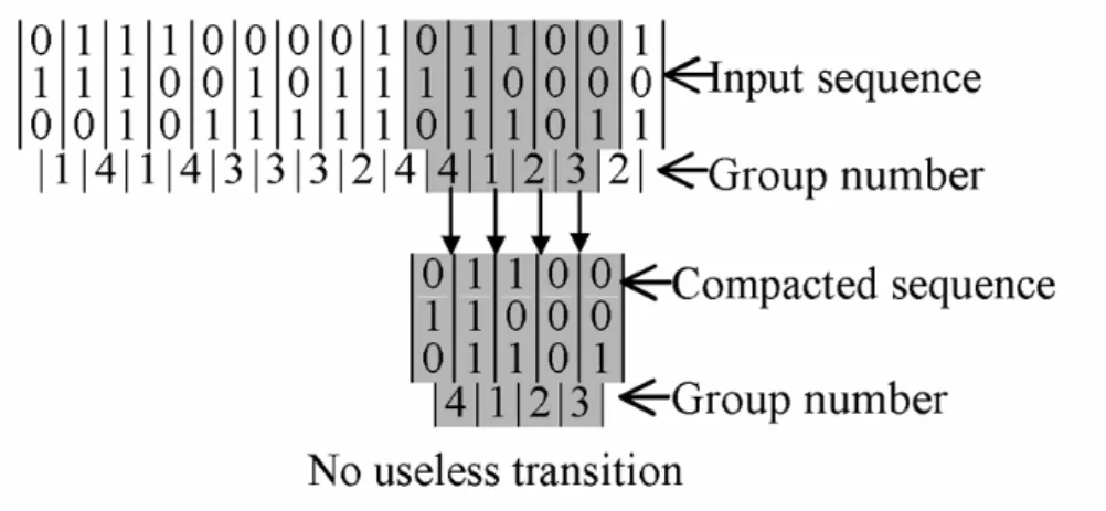
(34) 2.2 Useless Transitions For large circuits, vector compaction techniques could provide a faster solution for power estimation with reasonable accuracy. However, the random-liked sampling method may lose the compaction ratio and speedup as shown in Figure 2-1. Those group numbers in Figure 2-1 present different range of power characteristic values. After compaction, only 4 pattern pairs are randomly selected, one from each group. However, when those 4 pattern pairs are serially concatenated to be the compacted sequence, 7 pattern pairs will be found in the compacted sequence. That means the compaction ratio and speedup are lost because the compacted input sequence includes 3 useless transitions.. Figure 2-1. Random sampling with useless transition Therefore, we propose a single-sequence consecutive sampling technique to reduce those useless transitions. Using the single-sequence consecutive sampling technique as shown in Figure 2-2, we can sample a single period of patterns instead of individual pattern pairs to reduce the loss of compaction ratio caused by the useless transitions. Compared to the example shown in Figure 2-1, there is no useless transition in the compacted sequence so that we can keep the compaction ratio as desired and shorten the length of the sequence. 22.
(35) Figure 2-2. Consecutive sampling However, due to non-uniform distribution of pattern pairs in some groups, it is very possible that we cannot find a perfect consecutive sequence without any undesired transitions as shown in Figure 2-2. Using single-sequence consecutive sampling technique, we will over-sample some groups in such cases to find an intact single sequence that have enough samples for all groups. Therefore, the compaction ratio of the sequence length may not be improved too much. In those cases, if we can relax the limitation a little bit such that multiple consecutive sequences are allowed, we may generate a shorter sequence that still has the desired distribution. For example, if the desired distribution is G1:G2:G3:G4 = 3:1:2:2 for the input vectors shown in Figure 2-3, the compacted sequence found in single-sequence approach will include at least 11 transitions as shown in Figure 2-3(a). However, as shown in Figure 2-3(b), we can find two subsequences that also satisfy the requirements but the number of transitions is only 9 after concatenated. It implies that we can find better solutions for vector compaction problem if we minimize the number of sequences instead of setting the number to be one. Of course, the number of sequences could be one as handled in the original single-sequence approach, but it is just a special case in the multi-sequence approach. Therefore, in this work, we focus on discussing this new extension and perform some 23.
(36) experiments to show the improvements of this new approach.. Figure 2-3(a). The result of single-sequence approach. Figure 2-3(b). The result of multi-sequence approach In this work, our focus is to reduce useless transitions in random-liked sampling method for vector compaction. Although those vector compaction methods including previous approaches and the proposed approach only focus on combinational circuits, they can still be applied to sequential circuits with full scan. The only difference is that we have to record the internal states of all flip-flops (FFs) when we estimate logic-level power characteristics of each input transition. This FF information will then be used in the transistor-level simulation for the compacted input sequence to set the internal states at the beginning of each composing subsequence. Therefore, if the compacted input sequence is composed of only one subsequence, we only have to set the initial condition once, which requires very little overhead.. 2.3 Selection of Power Characteristics The power consumption of a CMOS digital circuit is often formulated as Equation (2-1). 24.
(37) The static power (Pstatic) is often much smaller than the dynamic power (Pdynamic). The Pdynamic is the summation of the functional transition power (Pfunc_trans), the glitch power (Pglitch) and the short-circuit power (Pshort-circuit), which is represented as Equation (2-2). The Pshort-circuit is consumed when short-circuit current flows from VDD to ground at the period that both PMOS and NMOS transistors turn on together during the signal transitions and is often smaller than the summation of the Pfunc_trans and the Pglitch. The proportion between Pfunc_trans and Pglitch depends on the circuit behavior and the design skill. Given a circuit with n nodes in its netlist, we could express the power consumptions of Pfunc_trans and Pglitch as Equation (2-3) and (2-4), where i denotes the index of each internal node, Ci is its load capacitance of node i, Vdd is supply voltage of the circuit, fi_func is the frequency of functional transition at node i and. fi_glitch is the frequency of glitch at node i. Note that a node in the netlist is defined as the input or output of a logic gate in the circuit. Generally speaking, a functional transition only considers the signal transition from 0 to 1 or 1 to 0. On the contrary, a glitch is the signal transition from 0 to 1 to 0 or 1 to 0 to 1 such that it is not multiplied by a factor 1/2. τi is the factor of the width of glitch to the glitch power and should be between 1 and 0.. P = Pstatic + Pdynamic. (2-1). Pdynamic = Pfunc _ trans + Pglitch + Pshort −circuit. (2-2). Pfunc _ trans =. 1 2 n ⋅ Vdd ⋅ ∑ Ci ⋅ f i _ func 2 i =1 n. (2-3). Pglitch = Vdd2 ∑ C i ⋅ f i _ glitch ⋅ τ i. (2-4). P = Pfunc _ trans + Pglitch + Pshort −circuit + Pstatic. (2-5). i =1. 25.
(38) n. In Equation (2-3), the term. ∑C ⋅ f i =1. i. i _ func. is often defined as the charging and. discharging capacitance (CDC) during an input transition, where fi_func =1 if node i has signal transition and fi_func =0 if node i has no signal transition. The Ci of node i is the summation of output capacitance for driving gate and the input capacitances of driven gates at node i. For commercial cell libraries, the vendors will provide the output loading capacitance and input loading capacitances of cells. If such loading information is not provided, users can easily characterize the loading capacitances by themselves using the characterization process proposed in [19]. Therefore, to calculate the CDC values of an input pattern pair only have to sum the loading capacitances of those nodes whose logic values are changed during the input transitions. Only a logic-level simulator is required to obtain the node transition information for calculating CDC values. In the simulation-based vector compaction approaches that consider the circuit structures or behaviors, they often classify the input pattern pairs according to some power characteristics of each pattern pair. In the literatures, many power characteristics have been proposed [23,24][27] [30]. For example, Hamming distance (HD) of pattern pairs is adopted in [23][27] which use the number of transition bits of the primary inputs to approximate the average power consumption. Switching count (SC) is used in [30] to approximate the power n. consumption of a pattern pair using the summation of. ∑f i =1. i _ func. . Charging and discharging. capacitance (CDC) is adopted in [40] to approximate the power consumption of a pattern pair. Power sensitivity is used in [24,27] as an estimation on the influence of an input to the overall power consumption. In the vector compaction approaches, the adopted power characteristics have large 26.
(39) impacts on the accuracy of the estimated power and the extra computation overhead for the compacted input sequences. In order to determine which power characteristic is most suitable for different circuits, we define the average normalized error of a power characteristic as below to make a fair comparison between them. An average normalized error (AVGNE) is the average error between the normalized power characteristics to the normalized real power of all combinations of input vectors. The normalized power characteristic is the power characteristic value divided by the average power characteristic value. The normalized real power is the power consumption divided by the average power. For a combinational circuit with n inputs, we can formulate the AVGNE of any power characteristic PC as Equation (2-6). In Equation (2-6), Pj,k is the power consumption of the transition from pattern j to pattern k, and PCj,k is the power characteristic value of that transition. Pavg is the average power consumption of all input pattern pairs and PCavg is the average power characteristic value of all input pattern pairs.. AVGNEPC =. 2n −1 2 n −1. 1 2. n+n. PCavg =. Pavg =. PC j ,k. ∑ ∑ | ( PC j =0 k =0. 1 2 n+ n 1 2 n+ n. avg. 2n −1 2n −1. ∑ ∑ PC j =0 k = 0. 2 n −1 2 n −1. ∑∑P j =0 k = 0. j ,k. j ,k. −. Pj ,k Pavg. )|. (2-6). (2-7). (2-8). The AVGNE of a power characteristic can make a fair comparison between the power characteristic value and the real power consumption. The power characteristic with smaller AVGNE is considered as much closer to the real power. Therefore, we make some 27.
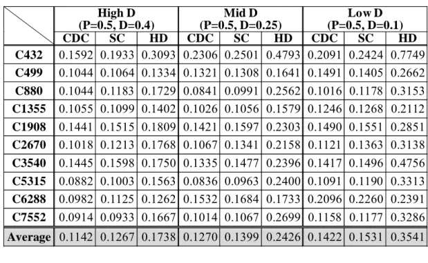
(40) experiments to evaluate the AVGNE of some popular power characteristics. In our previous work [79], we have compared the AVGNE of CDC and HD. In this work, we compare the AVGNE of three popular power characteristics, HD, zero-delay CDC and zero-delay SC. In our experiments, we evaluate the AVGNE by three input sequences with the same average input signal probability (P=0.5) but different average transition density (D) on several ISCAS’85 benchmark circuits. For the input sequence with high average transition density, D is set to 0.4. For the input sequence with middle average transition density, D is set to 0.25. For the input sequence with low average transition density, D is set to 0.1. For each test sequence, 500 pattern pairs are randomly generated according to the desired signal probability and transition density. Those patterns are then used in PowerMill to simulate their power consumptions. About the corresponding power characteristic values, the CDC and SC values are calculated by the Verilog-XL simulator, and the HD values is obtained by a simple self-developed C program. The comparison result is shown in Table 2-1. The AVGNEs of ISCAS’85 benchmark circuits are estimated by three test sequences and the overall average AVGNEs of CDC, SC and HD are 0.1278, 0.1399 and 0.2568 respectively. Therefore, we also choose CDC to be the power characteristic in this work.. 28.
(41) Table 2-1. Average normalized errors for three power characteristics. C432 C499 C880 C1355 C1908 C2670 C3540 C5315 C6288 C7552. High D (P=0.5, D=0.4) CDC SC HD 0.1592 0.1933 0.3093 0.1044 0.1064 0.1334 0.1044 0.1183 0.1729 0.1055 0.1099 0.1402 0.1441 0.1515 0.1809 0.1018 0.1213 0.1768 0.1445 0.1598 0.1750 0.0882 0.1003 0.1563 0.0982 0.1125 0.1262 0.0914 0.0933 0.1667. Mid D (P=0.5, D=0.25) CDC SC HD 0.2306 0.2501 0.4793 0.1321 0.1308 0.1641 0.0841 0.0991 0.2562 0.1026 0.1056 0.1579 0.1421 0.1597 0.2303 0.1067 0.1341 0.2158 0.1335 0.1477 0.2396 0.0836 0.0963 0.2400 0.1532 0.1684 0.1733 0.1014 0.1067 0.2699. Low D (P=0.5, D=0.1) CDC SC HD 0.2091 0.2424 0.7749 0.1491 0.1405 0.2662 0.1016 0.1178 0.3153 0.1246 0.1268 0.2112 0.1490 0.1551 0.2851 0.1121 0.1363 0.3138 0.1417 0.1496 0.4756 0.1091 0.1190 0.3313 0.2096 0.2260 0.2391 0.1158 0.1177 0.3286. Average 0.1142 0.1267 0.1738 0.1270 0.1399 0.2426 0.1422 0.1531 0.3541. 2.4 Grouping of Pattern Pairs If we have a power characteristic that is almost proportional to the real power consumption for all pattern pairs, we can easily generate a compacted input sequence for estimating the average power consumption of a circuit by a simple random selection. For example, if the original input sequence is L and the compacted sequence is C, the power consumption of the original input sequence PL can be calculated from PL=PC*(PCL/PCC), where PCL is the total power characteristic value of the original input sequence, PCC is the total power characteristic value of the compacted sequence, and PC is the power consumption of the compacted sequence. However, most of the power characteristics including CDC can only model the functional transition power. The glitch power is often not proportional to the functional transition power for all pattern pairs such that the power characteristic values may 29.
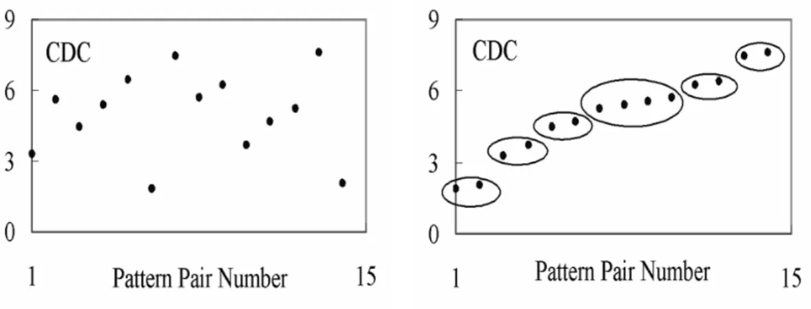
(42) not always be proportional to the real power consumption. Therefore, another solution is required instead of random selection to minimize the estimation errors. One popular approach is to separate the input pattern pairs into several groups according to their power characteristics and then sample pattern pairs from each group. This grouping method, which is also applied in this work, is widely used just like [40] with very low computation complexity. The variation caused by glitch power can be effectively reduced because the average value of each group is used to represent the power consumption of all pattern pairs that belong to this group such that the variation can be compensated. In order to demonstrate the grouping effects, we perform a simple experiment on C1355 in ISCAS’85 benchmark circuits with 5,000 random input pattern pairs. The variance limitation of each group is set as ±2.5%. The experimental results are illustrated in Figure 2-4 to show the estimation error between normalized CDC values and normalized real power values of all pattern pairs. The estimation error of each pattern pair is defined as Equation (2-9), where NCDCi is the normalized CDC value of pattern pair i, and NPi is the normalized power consumption of pattern pair i. Without grouping, all pattern pairs are treated as a single group with group number 0 in Figure 2-4. We can see that there is a large error distributed from 20% to -60%. After divided those pattern pairs into 24 groups with group number 1 to 24 in Figure 2-4, we can see that the error distribution range of each group is significantly reduced if the average value is used to represent the real power value of each pattern pair in the same group. Errori =. NCDCi − NPi × 100 NPi. 30. (2-9).
(43) Figure 2-4. The effects of grouping Figure 2-5 shows an example of the grouping process. Figure 2-5(a) is the distribution of the CDC values of 15 pattern pairs. After sorting and grouping, those pattern pairs with similar CDC values will be put together into a group as shown in Figure 2-5(b). In this example, there are six groups for the input pattern pairs. The group size and the number of groups is determined by a user-defined variance limitation, which is the range of CDC values in a group from the average CDC value to its maximum or minimum value.. (a). CDC distribution. (b). Sorting and grouping. Figure 2-5. An example of grouping process. 31.
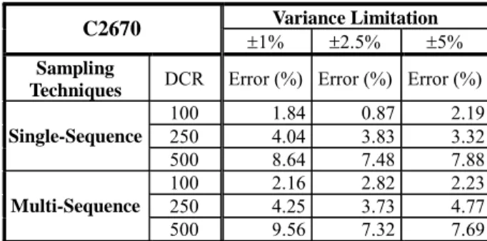
(44) Our experience shows that the best variance limitation falls between ±2.5% to ±5%. If the variance limitation is smaller than ±2.5%, the number of groups is increased and the group sizes are decreased. In this case, it is hard to obtain a high compaction ratio because many groups are too small to provide enough samples. If the variance limitation is larger than ±5%, the grouping process will cause larger errors because the glitch power may be quite different between those pattern pairs in a group. Therefore, there is a trade-off between the compaction ratio, the estimation error, and the variance limitation, which can only be decided according to the characteristics of the circuits. In order to demonstrate these effects, we use 50,000 pseudo random vectors to test C2670 in ISCAS’85 benchmark circuits with different variance limitation and compression ratio by using the two different vector compaction approaches that will be introduced in Section 2.5. The experimental results are shown in Table 2-2. In Table 2-2, DCR is the abbreviation of desired compaction ratio. From the results, we can see that the estimation errors will increase in both approaches when the compression ratio is increased. If we set the variance limitation to a smaller value (1%), we can see that the estimation errors are getting worst especially for high compression ratio because many groups are too small to provide enough samples. When the variance limitation is set to a larger value (5%), the estimation error will also increase because the variation in a group is increased.. 32.
(45) Table 2-2. The relationship between compaction ratio, variance limitation and estimation error Variance Limitation ±1% ±2.5% ±5%. C2670 Sampling Techniques Single-Sequence. Multi-Sequence. DCR. Error (%) Error (%) Error (%). 100 250 500 100 250 500. 1.84 4.04 8.64 2.16 4.25 9.56. 0.87 3.83 7.48 2.82 3.73 7.32. 2.19 3.32 7.88 2.23 4.77 7.69. The pseudo code of the grouping process is shown in Figure 2-6. The subroutine QuickSort() sorts all pattern pairs according to their CDC values. When we try to merge a pattern pair into the current group, the subroutine cal_group_avg_cdc() calculates the average CDC value of this group. And the subroutine violate_var_limit() will test whether the variance limitation is violated due to the added pattern pair. If this group will not violate the variance limitation with the added pattern pair, this pattern pair will be merged into the current group. Otherwise, a new group will be built in which this pattern pair is the first member. The grouping information will be recorded in a data structure group[] and the total number of groups will be returned after the whole process is finished.. 33.
(46) Grouping(pattern_pair[],N, var_limit,group[]) { QuickSort(pattern_pair[],N); group_num = 1; g_h=g_t=N; while(g_h > 0) { group_avg_cdc=cal_group_avg_cdc(pattern_pair[],g_h,g_t); if (violate_var_limit(group_avg_cdc,pattern_pair[g_h].cdc, pattern_pair[g_t].cdc,var_limit)) { group[group_num].size=g_t-g_h; group_num++; g_t=g_h; group_avg = pattern_pair[g_h].cdc; pattern_pair[g_h].group_num=group_num; } pattern_pair[g_h].group_num=group_num; g_h--; } return(group_num); }. Figure 2-6. The pseudo code of the grouping algorithm. 2.5 Consecutive Sampling techniques 2.5.1 Single-Sequence Approach After grouping, we can sample a number of pattern pairs from each group according to the size of the group divided by a user-defined compaction ratio. It is often called the proportional sampling strategy [27]. Instead, we can sample a single pattern pair from each group, which is called single sampling strategy [40]. The single sampling strategy can only be used if the power characteristic is a very precise approximation of the real power. However, it can achieve a very high compaction ratio. The proportional sampling strategy can be used. 34.
(47) without a very precise power characteristic but the compaction ratio may not be as high as the single sampling strategy. In traditional sampling methods, people sample some independent pattern pairs from each group and concatenate them into a continuous sequence for simulation. Therefore, the sequence will include about half useless transitions as shown in Figure 2-1. Using a state transition graph and selecting the Euler trails on it with enough samples could be an approach to reduce useless transitions. However, it can only be used when most of states and transitions have passed many times. In typical cases, not all parts of the state transition graphs will be visited many times such that we are hard to obtain enough samples. Therefore, in order to reduce the useless transitions in most cases, we propose a single-sequence algorithm to sample a sequence of consecutive pattern pairs from the original input sequence with the desired distribution and compaction ratio. The single sequence algorithm can be formulated as below. Problem formulation: Given a sequence S of length N with entries in a set G={g1,g2,…,gm},. where gi∈Z+ (1,2,…) for 1 ≤ i ≤ m, and a set T={t1,t2,…,tm} with ti∈ Z 0+ (0,1,2,…) for 1 ≤ i ≤ m and ti ≤ s(gi) for 1 ≤ i ≤ m, where s(gi) represents how many times that gi appears in S, find the shortest subsequence S’ in S such that all gi∈G can be found in S’ at least ti times. Solution: According to the problem formulation, we can see that the shortest subsequence. that satisfies the requirements will also satisfy the following two conditions. The first condition is that the corresponding group of the start point in the shortest subsequence must exactly appear as the requirement in T. If the corresponding group of the start point is larger. 35.
數據


+7


相關文件
In this chapter, a dynamic voltage communication scheduling technique (DVC) is proposed to provide efficient schedules and better power consumption for GEN_BLOCK
To reduce the leakage current related higher power consumption in highly integrated circuit and overcome the physical thickness limitation of silicon dioxide, the conventional SiO
To reduce the leakage current related higher power consumption in highly integrated circuit and overcome the physical thickness limitation of silicon dioxide, the conventional SiO 2
“Reliability-Constrained Area Optimization of VLSI Power/Ground Network Via Sequence of Linear Programming “, Design Automation Conference, pp.156 161, 1999. Shi, “Fast
A segmented current steering architecture is used with optimized performance for speed, resolution, power consumption and area with TSMC 0.18μm process.. The DAC can be operated up
The gain-tilt optical amplifier is used to increase the signal powers of short wavelength channels and decrease the signal powers of long wavelength channels so that the
The major task of the research is to provide a sort of automatic system solution for producing the RF Power module in fast and accuracy by several core module from
7.7 Representation of Functions by Power Series 7.8 Taylor and Maclaurin Series... Thm 7.4 (Absolute Value Thoerem) Let {a n } be a sequence of
