247
Structural and optical properties of ZnO films grown on silicon and
their applications in MOS devices in conjunction with ZrO
2as a gate
dielectric
S K NANDI†, S CHAKRABORTY, M K BERA and C K MAITI*
Department of Electronics and ECE, Indian Institute of Technology, Kharagpur 721 302, India
†Department of Electronics Engineering and Institute of Electronics, National Chiao Tung University,
Hsinchu 300, Taiwan, R.O.C.
MS received 3 July 2006; revised 20 April 2007
Abstract. Photoluminescence (PL) properties of undoped ZnO thin films grown by rf magnetron sputtering on silicon substrates have been investigated. ZnO/Si substrates are characterized by Rutherford backscat-tering (RBS), X-ray diffraction (XRD), Fourier transform infrared (FTIR), and X-ray photoelectron spectro-scopy (XPS). ZrO2 thin films have been deposited on ZnO using microwave plasma enhanced chemical vapour deposition at a low temperature (150°C). Using metal insulator semiconductor (MIS) capacitor structures, the re-liability and the leakage current characteristics of ZrO2 films have been studied both at room and high tem-peratures. Schottky conduction mechanism is found to dominate the current conduction at a high tempe-rature. Good electrical and reliability properties suggest the suitability of deposited ZrO2 thin films as an alter-native as gate dielectric on ZnO/n-Si heterostructure for future device applications.
Keywords. ZnO; ZrO2; PECVD; high-k gate dielectric; conduction mechanism. 1. Introduction
Now a days, ZnO film is receiving increased attention for various microelectronic applications. It has potential uses in photo detectors (Liu et al 2000), solar cells, and light emitting diodes (LEDs) (Jeong et al 2006). ZnO is a II– VI compound n-type semiconductor with a wide direct band of 3⋅3 eV (at room temperature) (Tang et al 2006) and has a hexagonal quartzite structure with space group P63mc,
and cell parameters of a = 0⋅3250 nm, c = 0⋅5206 nm (Kubo et al 2000). It has a large exciton binding energy of 60 meV (Marotti et al 2004) which indicates that ZnO is the material with most potential to realize the next gene-ration UV semiconductor laser. Silicon is not only of in-terest for the integration of optoelectronic devices but is also cheaper and easier to cleave in comparison with sap-phire, which is widely used as substrate in the deposition of ZnO film (Xu et al 2005).
The current trends in silicon metal–oxide–semiconductor field effect transistors (MOSFETs) scaling have indicated that new generation of devices are necessary beyond 2010 or so. As the device dimensions are scaled down, the gate dielectric thickness needs to be scaled and a 15 Å thick SiO2 will be necessary soon. However, due to high direct
tunneling current and reliability concerns, conventional
thermally grown silicon dioxide (SiO2) cannot be used as the
gate dielectric and an alternative is being researched into. High dielectric constant (high-k) gate dielectrics are needed to replace SiO2 by providing a physically thicker layer
and still maintain the same gate capacitance, while reducing the tunneling current.
Alternative high-k materials such as HfO2, Ta2O5, ZrO2,
TiO2 etc are currently under intense investigation. Among
them ZrO2 is a promising candidate for replacement of
SiO2 because it is a very promising material for optical
(for its high reflective index, low absorption coefficient, etc) and mechanical (for its hardness, durability, and low chemical reactivity) applications (Balog et al 1977; Rus-sak et al 1989; Khawaja et al 1993; Kralik et al 1998; Cameron and George 1999). In fact, ZrO2 has some very
attractive properties for microelectronics applications. It has a wide band gap of 5⋅16–7⋅1 eV (Balog et al 1977; French et al 1994); this wide band gap could result in high barrier height for tunneling and hence reduces the leakage current. It has a dielectric constant in the range 15–22, which is high enough to achieve lower equivalent oxide thickness (EOT).
To produce the electronic devices using ZnO films, it is essential to study the electrical and other properties such as structural reactions with high-k gate dielectrics deposited on it. Usually, the metal insulator semiconductor (MIS) structures are used for this purpose. For the realization of electronic devices, it is also important to understand the *Author for correspondence ([email protected])
stability, formation kinetics of the dielectric films and also their reliability on thin ZnO films. However, very little is known about the interfacial properties of gate dielectrics deposited on thin ZnO films. Chemical vapour deposition (CVD) techniques are commonly used to deposit dielectric films due to their superior step coverage over physical vapour deposition processes. The plasma enhanced CVD (PECVD) process has a distinct advantage over other thermal CVD methods in which a high deposition rate can be achieved at a low substrate temperature (Ray et al 1996; Raoux et al 1997).
In the present study, ZnO films were deposited by the conventional rf magnetron sputtering on silicon substrates, and the ZnO/Si structures are characterized by RBS, XRD, PL and FTIR. To the best of our knowledge, there has been no report on the electrical and interfacial properties of ZrO2/ZnO/n-Si structures. In this paper, we report on
the deposition of thin high-k ZrO2 films at a low temperature
on ZnO/n-Si substrates and the electrical properties of thin ZrO2 films as a gate dielectric both at room and high
temperatures. 2. Experimental
In this study, undoped ZnO (100 nm thick) thin films were grown on n-Si (100) at 450°C by rf magnetron sputtering of sintered commercial 2-inch ZnO targets (purity, ∼ 99⋅99%). Ar was introduced as a plasma gas and working pressure was 10 mTorr. After standard cleaning (RCA) of the ZnO/ n-type Si substrates followed by a dip in 1% HF, ZrO2
films were deposited by microwave (700 watt, 2⋅45 GHz) plasma cavity discharge system at a pressure of 500 mTorr and temperature of 150°C. For ZrO2 films deposition,
metalorganic zirconium tetratert butoxide [Zr(OC(CH3)3)4]
compound and O2were used as the source materials. The
thickness of ZrO2films (15 nm) was determined using a
single wavelength (632⋅8 nm) ellipsometer (Model: Gaertner L-117). The electrical properties of the deposited films were studied using Al/ZrO2/ZnO/n-Si MIS capacitors
with an Al gate (area: 1⋅96 × 10–3 cm2). The capacitance– voltage (C–V), conductance–voltage (G–V), and current– voltage (I–V) were measured using HP-4061A semiconductor test system and HP-4145B DC parameter analyser, respec-tively.
3. Results and discussion
Rutherford backscattering (RBS) analysis was carried out to estimate the composition and thickness of the films. 2 MeV He+2 beams, attained through a charge exchange process with a stripper nitrogen gas, is normally used for the RBS and channeling measurements. The energy momen-tum of the beam is gained from a 90° analysing magnet and the beam is directed to the scattering chamber through a switching magnet. The beam is collimated by a
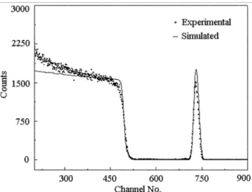
pair of collimators of diameter, 1 mm, separated by a dis-tance of about half a meter. This is done to reduce the divergence of the beam, which is important for channeling measurements. The surface barrier detector (SBD) (resolu-tion, 25 keV) can detect scattered particles over a scattering range of 0–170°. The solid angle subtended by SBD is maintained around 2 × 10⁻³ steradian with the target. The beam current is in the range 5–20 nA. The sample position with respect to the beam can be varied vertically without breaking the vacuum. The data are collected by a MCDWIN (Version-1.0) multichannel analyser attached to a data acquisition computer. Figure 1 shows a typical RBS spec-trum of ZnO/Si sample as described above. The scattered He+2 from the ZnO layer appears at higher energies (channel nos. 715–750) while those from the bulk Si sub-strate appear at lower energies (channel nos. 500–525). The experimental spectra were simulated using GISA 3.99. The thickness of ZnO layer was estimated to be 100⋅5 nm.
Figure 1. 2 MeV 4He2+ Rutherford backscattering spectra of ZnO/Si sample: (+++) experimental and (---) simulation.
Figure 2. X-ray diffraction pattern of the as-grown ZnO thin film at 450°C and rf power, 100 W.
ZnO films usually exhibit (002) orientation with c-axis perpendicular to the substrate due to the lowest surface free energy for (002) plane. Another preferred orientation, however, is difficult to form, but is of interest. It is seen that ZnO films with (103) orientations are deposited by rf magnetron sputtering as shown in figure 2. The angular peak position of deposited films with (002) orientation is located at 2θ = 34⋅1° (Nandi et al 2002). From XRD study it is clear that the deposited ZnO film is polycrystalline in nature. Now one can easily estimate the average crystallite size using the Scherrer’s equation:
. 0 9 cos D λ β θ = ,
Figure 3. Emission PL spectra of ZnO films at different tempe-ratures.
Figure 4. Integrated intensities of 380 nm and 502 nm emi-ssion peaks at different temperatures.
where λ is the wavelength of radiation used in XRD study, β the FWHM of the peak corresponding to (hkl) plane and θ the Bragg angle at peak position. Using the above relation the average crystallite size for (103) plane was estimated to be ~19⋅2 Ǻ.
To investigate the optical properties of films, photolumi-nescence (PL) measurements were performed. Although there are many reports concerning the luminescence properties of ZnO, for bulk samples and powder phos-phors, usually pressed in pellets and sintered at high tempe-rature (Vanheusden et al 1996), there are only a few reports concerning PL of ZnO films. Recently, ZnO films have attracted much interest because of its potential commercial application in ultraviolet (UV) laser since its optically pumped UV lasing was found at room tempera-ture (Bagnall et al 1997) and the PL properties of ZnO films have been studied widely. However, the excitation mechanism is not yet clear because a laser is usually used as the exciting source in most PL studies. Here, we ob-served the emission and excitation spectra of ZnO film using 325 nm HeCd laser as the exciting source with energy, 20 mW.
Under the 325 nm excitation, the PL emission spectra of a ZnO film at different temperatures are shown in figure 3. From the emission spectra, it is clearly found that there are two emission bands which peaked at 380 nm (UV band) and 502 nm (green band) for all. The origins of the 380 nm and 502 nm bands have been ascribed to the band edge radiative recombination and intrinsic defects (mostly O vacancy) of ZnO, respectively and many workers have reported similar results (Tanaka et al 1995; Gorla et al 1999; Shi et al 1999). From figure 3, it can be seen that the intensity of 380 nm and 502 nm emission decreases when the sample temperature is increased. When the temperature is above 100 K, the 502 nm emission disappears. Also, the intensity of 380 nm increases as the sample temperature increases until it reaches 200 K and then decreases. The
Figure 5. FTIR spectrum of ZnO film deposited on silicon substrate at 450°C.
integrated intensities of 380 and 502 nm emission peaks at different temperatures are shown in figure 4, which were
Figure 6. (a) Broad scan XPS spectrum of ZrO2/ZnO/Si film showing characteristic peaks of Zn, O, C, Zr and Si, (b) decon-voluted O1 s and (c) typical Zr 3d spectra of ZrO2/ZnO/Si film.
calculated from the area under the curves of related emission peaks in figure 3.
Fourier transform infrared spectrum is the characteristic of a particular compound providing information about its functional groups, molecular geometry and inter/intra-molecular interactions. The infrared spectrophotometer provides a record of the infrared absorbency or transmit-tance of a sample as a function of wave number. The fre-quencies at which absorption occurs may indicate the type of functional groups present in the substance. Fourier transform infrared spectroscopic (FTIR) measurements in the wave number range between 400 and 1000 cm–1 were carried out using Nicolet Magana IR750, FTIR spectrome-ter. In this spectrum (shown in figure 5), the absorbance band is situated at 411⋅5 cm–1. This band corresponded to the Zn–O stretching vibration for a tetrahedral surrounding of the zinc atoms (Bachari et al 2001).
XPS study was carried out using a model ESCALAB MKII high vacuum system equipped with a concentric hemispherical analyser (VG Microtech) with a residual gas pressure of ~1 × 10⁻⁸ Pa. MgKα X-ray (hν = 1253⋅6 eV)
radiation was used to excite the photoelectrons at an an-gle of 30° between the analyser axis and the sample nor-mal. All spectra were taken at 300 K (room temperature). The broad energy XPS spectra of the films are shown in fig-ure 6(a). It is observed that peaks are found to be at 100 eV for Si 2p, 149 eV for Si 2s, 182 eV for Zr 3d, 284 eV for C 1s, 532 eV for O 1s, 1022 eV for Zn 2p3/2
and 1045 eV for Zn 2p1/2. Figures 6(b) and (c) show the
high-resolution XPS spectra of O 1s and Zr 3d, respecti-vely. Figure 6(b) shows the measured O 1s peak, which can be deconvoluted into two sub peaks at 531⋅8 eV and 529⋅7 eV, assigned to –OH and Zn–O bonding, respecti-vely (Ayouchi et al 2003). Figure 6(c) shows the core-level spectrum of Zr 3d at binding energies, 182⋅3 eV for Zr 3d5/2 and 184⋅6 eV for Zr 3d3/2. The peak of Zr 3d5/2 at
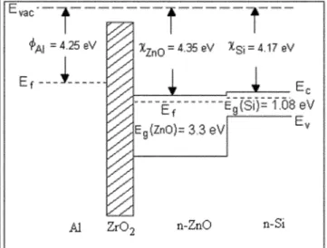
Figure 7. Energy band alignment in Al/ZrO2/ZnO/n-Si MIS capacitor.
182⋅3 eV is a typical characteristic of the Zr4+ in ZrO2
(Sun et al 2000).
The high frequency C–V characteristics of Al/ZrO2/ZnO/
n-Si in figure 8 (in inset) can be explained from the band diagram as shown in figure 7. From the band diagram it can be shown that the MIS capacitor will be in the inversion region at zero gate bias due to the favourable work func-tion difference between the Al gate and ZnO. Interface trap density distribution throughout the band gap is evaluated by a high frequency method developed by Terman (1962). This method relies on capacitance–voltage measurement at a high frequency where interface traps are assumed not to respond to the a.c. signal but do respond to the varying d.c. voltages, and cause the C–V curve to stretch out along the voltage axis. This stretch-out effect produces a non-parallel shift of the C–V curve.
The interface trap density (Dit) is determined from the
difference between the ideal and experimental ψs vs Vg
curves by g ox it s ( ) , d V C D q dψ Δ = (1)
where ΔVg is the voltage shift of the experimental curve
with respect to ideal behaviour at each value of C, Cox the
oxide areal capacitance, ψs the surface potential, and q
the electronic charge. An interface trap density of 2⋅4 × 1011 cm–2 eV–1 was calculated for the sample at midgap as shown in figure 8.
From the high frequency (1 MHz) capacitance–voltage characteristics presented in figure 8 (in inset), the depletion depth (XdHF) and apparent doping (NappHF) as a function of
applied gate potential (VG) are obtained as (Voinigescu et
al 1994)
Figure 8. Energy distribution of density of interface states of Al/ZrO2/ZnO/n-Si MIS capacitor (inset: high frequency C–V
characteristics). dHF G ZnO HF G ox 1 1 ( ) , ( ) X V C V C ε ⎛ ⎞ = ⋅⎜ − ⎟ ⎝ ⎠ (2) 2 H F G ZnO appH F G G 1 ( ) 1 , ( ) 2 C V q N V V δ ε δ ⎛ ⎞ ⎜ ⎟ ⎜ ⎟ ⎝ ⎠ = ⋅ (3)
where εZnO is the ZnO permittivity, 9 (Sze 1979). Cox is
the gate oxide capacitance per unit area, CHF(VG) the voltage
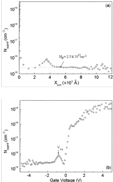
dependent capacitance per unit area of the heterostruc-ture, and q the electronic charge. The approximate sub-strate doping concentration (NB) of ≈ 2⋅5 × 1015 cm–3 is
obtained from a plot of NappHF vs XdHF as shown in figure
9(a). The threshold voltage of the ZnO/Si interface (VTH)
has been extracted from the C–V characteristics (figure 9(a)) and from the plot of NappHF vs V (figure 9 (b)). The
measured value of Vth is found to be –0⋅8 V.
Figure 9. (a) Experimental apparent doping concentration vs distance from the ZnO/Si interface and (b) apparent doping vs gate voltage characteristics from the ZnO/Si interface.
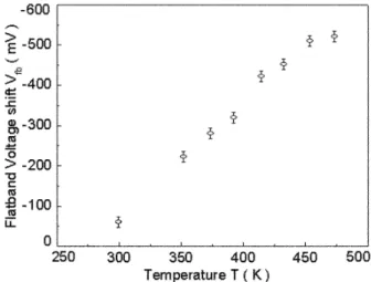
To study the thermal stability of the dielectrics, high frequency (1 MHz) C–V and G–V were performed in the temperature range 27–200°C and the results are shown in figure 10. It is observed that the C–V and G–V curves shift towards the left as the device temperature is increased from 27–200°C. The flat band voltage (Vfb) is found to
increase (more negative) with increasing device tempera-ture as shown in figure 11, which indicates the generation of positive charges in the oxide. This may be due to the presence of hole trapping centres in the films.
The gate current density (J) as a function of voltage across the gate (V) for the ZrO2/ZnO/n-Si layer is shown
in figure 12(a), from room temperature up to 200°C. It is observed that the current density of the films is strongly temperature dependent at low field, i.e. for E < 1 MV/cm, while its temperature dependence is much weaker at higher voltage. In figure 12(b), we show the temperature depend-ence of the conductance current at two electric fields,
Figure 10. High temperature measurement of (a) normalized capacitance and (b) conductance for MOS capacitors on ZnO films.
0⋅4 MV/cm and 2⋅7 MV/cm (Yassine et al 1999), respec-tively. This is also known as Arrhenius plot. The Schottky
Figure 11. Flat band voltage shift vs temperature characteristics.
Figure 12. Current density, J, as a function of electric field across the gate dielectric of Al–ZrO2–ZnO/n-Si MOS capa-citors: (a) recorded at room temperature to 200°C and (b) cur-rent density, J vs inverse of temperature for fixed applied electric fields, E, of 0⋅4 MV/cm and 2⋅7 MV/cm, respectively.
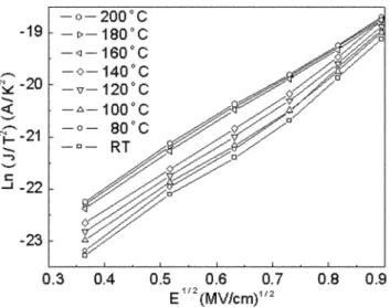
Figure 13. The ln J/T2 vs E1/2 plot for a MIS capacitor at dif-ferent temperatures showing Schottky conduction.
Figure 14. The ln(J/E) vs E1/2 is plotted for the MIS capa-citor. The straight line characteristic at relatively high electric field (≤ 1⋅1 MV/cm) indicates Poole–Frenkel conduction.
emission (SE), Poole–Frenkel (PF) emission, FN tunnel-ing, direct tunneling and space-charged limited mecha-nism are used to explain the basic conduction process in insulators. The SE process is due to the thermionic emis-sions across the metal–insulator-interface, which is res-ponsible for carrier transport.
The thermionic emission models range in various levels of physical complexity. The Schottky–Richardson relation is given for the J–E relation for Schottky emission,
2 b RD exp q exp E , J C T kT kT β ⎡ ⎤ − Φ ⋅ ⎡ ⎤ = ⋅ ⋅ ⎢ ⎥⋅ ⎢ ⎥ ⎣ ⎦ ⎣ ⎦ (4)
where β= q3/ 4πε ε0 i and CRD the Richardson constant.
Equation (4) can be written as
2 b RD ln( /J T ) ln(C ) q E. kT kT β Φ ⋅ = − + (5)
The plot of ln(J/T2) vs E is a straight line with a slope, β/kT. From figure 13, one can observe that the experi-mental plot of ln(J/T2) vs E with temperature as a para-meter is a straight line, which follows the SE mechanism at low electric field (≤ 0⋅65 MV/cm). The conduction properties of these films were further studied by plotting the data in terms of PF mechanism (Sze 1979) at higher electric fields. When the top electrode (gate) is positively biased, i.e. the holes are injected from the gate, the leakage current in the films can be well fitted by ln(J/E) vs E1/2 plot, indicating that the conduction is PF mechanism in the high field range (1⋅10–1⋅60 MV/cm) as shown in figure 14.
4. Conclusions
In summary, undoped polycrystalline ZnO (100 nm) thin films were deposited on n-Si (100) at 450°C by rf magne-tron sputtering. It is shown that the low temperature micro-wave PECVD techniques are useful for the deposition of good quality high-k ZrO2 gate dielectric directly on ZnO/
n-Si for future MIS applications. High temperature con-duction mechanism is found to be dominated by Schottky emission at low electric field while the Poole–Frenkel emission takes over at high electric field.
Acknowledgement
The ZnO/Si samples were prepared by Dr S Maikap. References
Ayouchi R, Leinen D, Martin F, Gabas M, Dalchiele E and Barrado J R R 2003 Thin Solid Films 426 68
Bachari E M, Amor S B, Baud G and Jacquet M 2001 Mater. Sci. Eng. B79 165
Bagnall D M, Chen Y F, Zhu Z, Yao T, Koyama S, Shen M Y and Goto T 1997 Appl. Phys. Lett. 70 2230
Balog M, Schieber M, Michman M and Patai S 1977 Thin Solid Films 47 109
Cameron M A and George S M 1999 Thin Solid Films 348 90 French R H, Glass S J, Ohuchi F S, Xu Y N and Ching W Y
1994 Phys. Rev. B49 5133
Gorla C R, Emanetoglu N W, Liang S, Mayo W E, Lu Y, Wra-back M and Shen H 1999 J. Appl. Phys. 85 2595
Jeong W J, Kim S K and Park G C 2006 Thin Solid Films 506– 507 180
Khawaja E E, Bouamrane F, Hallak A B, Daous M A and Salim M A 1993 J. Vac. Sci. & Technol. A11 580
Kralik B, Chang E K and Louie S G 1998 Phys. Rev. B57 7027 Kubo M, Oumi Y, Takaba H, Chatterjee A, Miyamoto A, Kawa-saki M, Yoshimoto M and Koinuma H 2000 Phys. Rev. B61 16187
Liu Y, Gorla C R, Liang S, Emanetoglu N, Lu Y, Shen H and Wraback M 2000 J. Electron. Mater. 29 60
Marotti R E, Guerra D N, Bello C, Machado G and Dalchiele E A 2004 Sol. Energy Mater. & Sol. Cell 82 85
Nandi S K et al 2002 Electron. Lett. 38 1390
Raoux S, Cheung D, Fodor M, Taylor W N and Fairbairn K 1997 Plasma Sources Sci. Technol. 6 405
Ray S K, Maiti C K, Lahiri S K and Chakrabarti N B 1996 Adv. Mater. Opt. Electron. 6 73
Russak M A, Jahnes C V and Katz E P 1989 J. Vac. Sci. & Technol. A7 1248
Shi C, Fu Z, Guo C, Ye X, Wei Y, Deng J, Shi J and Zhang G 1999 J. Electron. Spectrosc. & Rel. Phenom. 101–103 629 Sun Y M, Lozano J, Ho H, Park H J, Veldman S and White J M
2000 Appl. Surf. Sci. 61 115
Sze S M 1979 Physics of semiconductor devices (Wiley Eastern Limited)
Tanaka S, Takahashi K, Sekiguchi T, Sumino K and Tanaka J 1995 J. Appl. Phys. 77 4021
Tang Z K, Kawasaki M, Ohtomo A, Koinuma H and Segawa Y 2006 J. Cryst. Growth 287 169
Terman L M 1962 Solid State Electron. 5 285
Vanheusden K, Warren W L, Seager C H, Tallant D R, Voigt J A and Gnade B E 1996 J. Appl. Phys. 79 7983
Voinigescu S P, Iniewski K, Lisak R, Salama C A T, Noel J P and Houghton D C 1994 Solid State Electron. 37 1491 Xu W, Ye Z, Zhu L, Zeng Y, Jiang L and Zhao B 2005 J. Cryst.
Growth 277 490
Yassine A, Nariman H E and Olasupo K 1999 IEEE Electron. Dev. Lett. 20 390