國 立 交 通 大 學
光電工程研究所
博 士 論 文
主動顯示器用低溫多晶矽薄膜電晶體之元件特性
與補償電路研究
Study on Characterization and Compensation Circuits of
Low-Temperature Polycrystalline Silicon Thin-film
Transistor for Active Matrix Displays
研 究 生:盧皓彥
指導教授:祁 甡 教授
張鼎張 教授
主動顯示器用低溫多晶矽薄膜電晶體之元件特性
與補償電路研究
Study on Characterization and Compensation Circuits of
Low-Temperature Polycrystalline Silicon Thin-film
Transistor for Active Matrix Displays
研 究 生: 盧皓彥
Student: Hau-Yan Lu
指導教授: 祁 甡 博士
Advisor: Dr. Sien Chi
張 鼎 張 博士
Dr.Ting-Chang Chang
國 立 交 通 大 學
光電工程研究所
博 士 論 文
A Dissertation
Submitted to Institute of Electro-Optical Engineering
College of Electrical and Computer Engineering
National Chiao Tung University
In Partial Fulfillment of the Requirements
For the Degree of
Doctor of Philosophy
In Electro-Optical Engineering
June 2008
Hsin-chu, Taiwan
i
主動顯示器用低溫多晶矽薄膜電晶體之元件特
性與補償電路研究
研 究 生: 盧皓彥
指導教授: 祁 甡 博士
張 鼎 張 博士
國 立 交 通 大 學
光電工程研究所
摘要
本論文首先提出一種具有金屬遮光層(Metal shielding layer)的新穎低溫多晶 矽薄膜電晶體元件結構。於玻璃基板上先沉積一層金屬薄膜,並依序沉積緩衝層 (Buffer layer)與非晶矽薄膜,再利用主動層之光罩進行一次蝕刻,如此並不會增 加光罩數,此遮光層可以阻擋背光照射到多晶矽層,完全消除光漏電與次臨界擺 幅(Sub-threshold swing)於背光環境下之劣化,然而,此新式結構低溫多晶矽薄膜 電晶體之臨界電壓於暗態下會隨著汲極電壓而飄動,由於金屬遮光層與汲極電極 互相重疊,形成一寄生電容,汲極電壓會經由此寄生電容耦合至金屬遮光層中, 造成一電壓分佈於其中,進而影響元件之臨界電壓;為了消除此一問題,我們將 金屬遮光層利用額外一道光罩來定義其圖案,並研究此部分金屬遮光層位於通道 中央或接面區之元件特性,具有部分金屬遮光層之元件,無論遮光層位於哪一區,
ii 其臨界電壓皆不再隨汲極電壓而改變,此外,當部分金屬遮光層位於汲極接面區 時,能夠有效的抑制光漏電流之大小,反之,置於源極接面區或中央通道區之部 分遮光層皆無降低光漏電流之功效,然而,一旦施加大的汲極電壓,位於汲極接 面之金屬遮光層其遮光效果便會減弱,我們亦根據所獲得之實驗數據提出了一合 理模型來解釋此現象。 此外,我們亦嘗試對緩衝層之成分與其表面進行調變來抑制光電流的產生, 本論文提出了一種可吸收光源之介電層作為緩衝層,可將大部份之背光吸收,所 以多晶矽層所吸收的光強度便會減少,進而達到降低光漏電的效果,此光吸收緩 衝層主要為富含矽(Si-rich)之二氧化矽層或是矽化氮層,實驗發現,富含矽介電 層之光吸收能力與其薄膜厚度成正比,不論是使用富含矽之二氧化矽層或是矽化 氮層來製作元件,皆可達到30%~50%的光漏電流改善。此外,本論文亦對 一般緩衝層之表面進行氨電漿(NH3 plasma)處理,利用氨電漿對緩衝層表面進行 轟擊(Bombardment),使其表面裂化以產生大量之介面缺陷,此製程不僅不需要 增加額外的光罩數,且可以完全相容於一般標準製程,而緩衝層表面電漿處理過 之元件其基本特性與主要參數皆與標準元件相同,沒有金屬遮光層結構臨界電壓 飄移的問題,如此一來,光激發出的電子-電洞隊將可透過多晶矽薄膜與緩衝層 介面之缺陷密度進行複合,可有效降低光漏電與改善照光下之元件次臨界擺幅。 本論文也研究探討多晶矽薄膜電晶體元件於照光下之光漏電與次臨界擺幅 增加的物理機制,首先將緩衝層利用氬離子(Argon)佈植進行表面轟擊,使多晶 矽薄膜與緩衝層介面產生許多缺陷密度,我們發現經由緩衝層表面轟擊之元件, 其光漏電與照光下次臨界擺幅特性具有顯著的改善,由於多晶矽薄膜吸收被光後 會產生許多電子-電洞對,透過引入之缺陷密度可減少光致電子與電洞,因而造 成較低的光漏電流與較佳的次臨界擺幅,此外,一種新式的測式結構亦在本論文 中被提出,利用圖案化之金屬遮光層結構,我們可定義照光區於汲極或源極接面 區,其中當照光區位於源極接面且施加大汲極電壓時,照光下次臨界擺幅有著顯 著的上升,因此,根據此實驗結果,可推論次臨界擺幅於照光下之機制並於本論 文中提出物理模型與能帶圖以解釋之。
iii 由於多晶矽薄膜電晶體能夠整合週邊驅動電路進而由於多晶矽元件應用於 面板週邊驅動邏輯電路時,需要考量到多晶矽元件可靠度的問題,本論文中亦以 電容-電壓法(Capacitance-Voltage measurement)來研究低溫多晶矽薄膜電晶體於 交流操作下之可靠度,研究中發現交流訊號測試會造成元件導通電流嚴重的下降, 但其起始電壓變化並不大,同時汲/源極寄生電阻的也急劇增加,此外,元件劣 化後之低頻電容電壓曲線無明顯變化,但高頻下之電容電壓曲線卻隨著閘極正電 壓而變化,說明了多晶矽薄膜電晶體於交流操作下之劣化機制主要為淺態能階 (Tail state)的增加而深態能階(Deep state)密度並無太大變化,同時透過電容電壓 曲線,我們也發現交流訊號所產生之淺態能階為對稱分佈於源極與汲極。此外, 具有橫向結晶之低溫多晶矽元件於交流訊號下之可靠度亦在此論文中被研究,我 們可以將橫向結晶晶晶界(Grain boundary)分為主晶界(main-GB)與次晶界 (sub-GB),主晶界的特徵在於其分布方向垂直元件通道,並且為一突起(Protrusion) 結構;次晶界則是平行通道方向且較平坦,論文中挑選兩種較明顯對比之電晶體 進行分析,GB-TFT 為一含有主晶界在通道中央,NGB-TFT 中則僅有次晶界存 在,經過施加交流訊號測試,發現 GB-TFT 之劣化情形較 NGB-TFT 嚴重,我們 量測了此兩種元件之電容電壓曲線並進行通道電場電腦模擬,發顯 GB-TFT 之突 起結構將會造成尖端電場效應,使得此區聚集的載子較多,進而在源極與汲極兩 端之高電場下造成元件的劣化。 本論文也提出了一種用於有機電激發光顯示器(AMOLED)之補償畫素電路 設計,此電路設計包含了五顆低溫多晶矽薄膜電晶體與一儲存電容結構,由於低 溫多晶矽薄膜電晶體其均勻度受到結晶晶界的影響,畫素之間的元件特性皆不相 同,使得各畫素輸出亮度會友不均勻的情形,同時,由於金屬導線之電阻效應會 造成電壓供應端(VDD)經過長距離導線時產生一電壓下降的現象,此現象亦會造 成有一電激發光顯示器畫面亮度有沿著某方向遞減的情形,本論文所提出的畫素 電路與新補償方法可在一次操作中同時消除元件臨界電壓飄移與電壓源下降所 導致之輸出電流變動,經由 HSPICE 軟體的驗證,此電路設計可用於高解析度與
iv 大尺寸之有機電激發光顯示器中。 本論文最後研究提出一種利用非晶矽薄膜電晶體之有機電激發光顯示器畫 素設計,由於非晶矽薄膜電晶體具有良好的元件均勻度與相當低的製造成本,非 常適合做為有機電激發光顯示器之背板(Backplane),然而非晶矽薄膜電晶體之臨 界電壓會隨著操作時間而上升,且有機電激發光二極體之起始電壓亦有隨著使用 時間增加的趨勢,造成輸出亮度之下降,此新式非晶矽薄膜電晶體畫素設計利用 源極隨耦器(Source follower)之概念,不僅結構與補償步驟簡單,並可同時補償元 件臨界電壓與有機電激發光二極體起始電壓的影響,可應用於大尺寸有機電激發 光顯示器。
v
Study on Characterization and Compensation
Circuits of Low-Temperature Polycrystalline
Silicon Thin-film Transistor for Active Matrix
Displays
Student: Hau-Yan Lu
Advisor: Dr. Sien Chi
Dr. Ting-Chang Chang
Department of Photonics & Institute of Electro-Optical Engineering
College of Electrical and Computer Engineering
National Chiao Tung University
Abstract
A novel technology to eliminate the photo leakage current of poly-silicon thin film transistor (poly-Si TFT) with top gate is developed. A thin metal film is formed on the glass substrate to be used as light-shielding layer. The light-shielding layer, buffer layer and active island are patterned by employing the same mask. The leakage current and the variation of sub-threshold swing in the proposed devices are suppressed completely under illumination. Owing to the parasitic capacitance in the overlap region between the drain side and the metal shielding layer, a floating voltage coupled from drain bias would influence the threshold voltage of the proposed poly-Si TFTs. In order to solve this issue, a partial metal shielding structure for poly-Si TFT is
vi
studied. The metal shielding layer is formed and etched to be located in the channel region and junction regions. According to this structure, the shift of threshold voltage with increasing drain bias is entirely eliminated. Furthermore, the photo leakage current of poly-Si TFT with partial metal shielding layer located in the drain junction is suppressed. However, the shielding effect is vanished as the drain voltage is high. Based on these data, this study also proposes a model to explain the mechanism of partial metal shielding layer located at drain side for lowing photo leakage current.
In addition, poly-Si TFT with light absorption structure is proposed to lower the photo leakage. No need of adding process steps or number of masks, the oxide film or SiNX film of buffer layer is replaced by Si-rich dielectric films. By this method, the
photo leakage can be markedly lowered and the degradation of sub-threshold swing is also reduced. It is observed that the light absorption capacity of Si-rich dielectric material is strongly proportional to the film thickness. In addition, the technology of poly-Si TFTs with low photo leakage current is developed in this work. The electrical characteristics of poly-Si TFT under illumination were significantly improved employing the NH3 plasma treatment on the buffer layer, no need for complicate
device structure and additional masks. The generation of trap states originated from the plasma bombardment on the interface between poly-Si layer and buffer oxide can effectively recombine the light-induced electron-hole pairs. The fewer residual electron-hole pairs in the bottom of poly-Si layer leads to the lower photo leakage current and improved sub-threshold swing, as well as also maintain the good electrical characteristics in the dark sate.
Next, poly-Si TFTs with different process flows are used to investigate the electrical characteristics under illumination. First, the surface of buffer layer of poly-si TFT is degraded by Argon ion implant to generate plenty of trap densities on the interface of poly-Si layer and buffer layer. The photo leakage current and the
vii
degradation of sub-threshold swing are improved substantially, compared to the conventional poly-Si TFT. It is attributed to that the light induced electron-hole in the bottom of poly-Si film may be recombined directly via the surface state densities. Therefore, the fewer electrons and holes lead to the lower photo leakage current and less increase of sub-threshold swing, respectively. Moreover, The electrical characteristics of poly-Si TFTs with patterned metal shielding layer under illumination are investigated in this study. The location of the exposure region in poly-Si layer is well defined by employing the proposed structure. The photo leakage current increases obviously as the exposure region is located in drain junction. Therefore, the drain junction under light exposure is effective region to induce the photo leakage current. However, the sub-threshold swing of TFT under illumination is significantly degraded while the exposure region is located in source junction with high drain voltage. It is indicated that the key factors to affect the sub-threshold swing is the residual excess holes accumulated in source junction. From the results of poly-Si TFT with degraded buffer layer and partial metal shielding layer, the model for mechanism of increased sub-threshold swing under illumination is proposed.
The electrical degradation of n-channel poly-Si TFT has been investigated under dynamic voltage stress by capacitance-voltage (C-V) measurement. In C-V measurements, the fixed charges in the gate oxide film of TFTs are not affected by the applied small signal, whereas the trap states in the band gap would respond to the applied frequency, so that the dominant degradation mechanism of poly-Si TFTs can be evaluated. Our experimental results show that the degradation of n-type TFTs is caused by additional trap states located at the drain and the source junction in the poly-Si thin film. Furthermore, through the experimental results of the C-V characteristics measured at 10 kHz and 1 MHz, we can infer that the tail states produced by the strained bounding in poly-Si film are mostly responsible for the
viii
electrical degradation of n-channel poly-Si TFTs after dynamic stress. In addition, this
work also studies the electrical degradation of laterally grown poly-Si TFTs under
dynamic voltage stress. The experimental results show the severity of the degradation
of poly-Si TFTs with a protruding grain boundary. The concentration of the electric
field in the protrusion region was verified by capacitance-voltage measurements and
simulation of the device characteristics. These results reveal that more electrons are
induced at the grain boundary of the poly-Si channel because of the relatively high
electric field in the protrusion region. Based on these data, this study proposes a
model to explain the enhanced electrical degradation of poly-Si TFTs with a
protruding grain boundary, generated by laser-crystallized lateral growth technique.
A new pixel design and driving method for active-matrix organic light emitting diode (AMOLED) display using poly-Si TFT is proposed. The new circuit consists of five TFTs and one capacitor to eliminate the variation in the threshold voltage of the TFTs, and the drop in the supply voltage in a single frame operation. The proposed pixel circuit has been verified to realize uniform output current by the simulation work using HSPICE software. The simulated error rate of the output current is also discussed in this paper. The novel pixel design has great potential for use in large size and high resolution AMOLED displays. Finally, this work also presents a new a-Si:H pixel circuit with source-follower type compensation method for large-size AMOLED displays. The proposed pixel circuit consists of five TFTs and one capacitor to compensate the shift in the threshold voltage of the driving TFT and OLED used in AMOLED and the compensation process is simplified by the proposed driving scheme. The high immunity to degradation of TFT and OLED in proposed pixel has been verified by the simulation work using HSPICE software. The novel pixel design has great potential for use in large-size AMOLED displays.
ix
誌 謝
蟬聲唧唧,又是一個雨後的夏夜,數不清已度過多少個這樣的夜晚,但我知 道,求學之路即將前往一個終站,心中百感交集,有著說不完的感激與溫暖,腦 海裡盡是一路走來所收藏的珍貴回憶,許許多多的人事物,與我交織出一幕幕精 彩豐富的瞬間,如幻燈片般歷歷在目,一切彷彿昨日般鮮明,轉眼間卻離我十分 遙遠,降落在最深層的思緒當中。在交大博士班修業的這些年裡,首先要特別感 謝兩位指導教授-祁甡教授與張鼎張教授,在兩位老師孜孜不倦的教誨與鼓勵下, 使我能夠不斷成長並得以一窺知識的殿堂,進而完成論文。祁教授時常的關心與 照顧,讓我備感窩心,給予學生莫大的空間進行學術研究,讓我得以發揮所長, 是一個祥和博學的長者。張鼎張教授多年來不辭辛勞的指導我論文研究,每當思 路遇到瓶頸,張教授總能指引學生一條饒富創意與邏輯的康莊大道,使我豁然開 朗,而張教授積極的態度與研究的熱忱,亦讓學生獲益匪淺。能夠於兩位師長的 指導下完成論文,實在是無比榮幸。 再者,由衷感謝劉柏村教授這些日子以來對於論文寫作與答辯技巧的指導, 劉老師總能提出學生思慮不周之處並耐心指正,並不厭其煩的與學生討論,著實 讓我的腳步站得更快更穩。在埋首於課業的這些寒暑中,一路上皆有許多幫助我 的人,特別感謝陳紀文學長,引領我進入這浩瀚學海,並不吝於與我分享討論, 學長圓融的處事與樂觀進取的人生觀,讓我十分欽佩,此外,陳宏澤學長適時的 提出寶貴的建議與想法,十分熱心,這份亦師亦友的情誼,我也感念在心頭。也 要感謝友達光電提供實驗上的協助,讓我的論文更加充實與順暢。 在實驗室與許多夥伴努力奮鬥的回憶永難忘懷,非常感謝這些學長、弟妹們: 永俊、峻豪、世青、敏全、大山、承丘、宏光、育德、威廷、超駿、晉瑋、宛芳、 子怡、建名,有了你們的幫忙與扶持,讓論文順利完成,另外,也要感謝正在與 實驗奮鬥的夥伴們:泓緯、興華、士哲、彥甫、立偉、一德、昭正、志瑋與其他 所有的碩士班學弟妹,有了你們的陪伴,讓我在平日的研究生活中,增添一抹歡x 笑的色彩,謝謝你們,要感謝的人實在太多,還有一些好朋友們,在這段日子裡 與我分享喜怒哀樂,感謝你們在背後默默的支持。 能夠走到這裡,我要感謝對我全心全意、默默付出的父親母親,盧士輪先生與 曹足女士,特別是我的母親,付出了一輩子的辛勞,只願讓我無後顧之憂的完成 學業,對我無微不至的照顧,在此特別獻上這本論文,希望能讓她心中感到無比 的驕傲與喜悅,而親愛的姐姐,我也要感謝你的愛護與叮嚀,十分溫暖。 感謝上天,在我求學生涯即將結束之時,讓女朋友曙如悄然降臨在我的身邊, 為原本靜謐黑暗的夜晚,綻放出五彩繽紛的火花,使我的生活多采多姿,煥然一 新,心靈更加祥和安定,感謝我最愛的曙如,有妳的支持,讓我的腳步更加堅定。 這個夏天依舊炎熱,電資大樓前的荷花依舊盛開,而我即將離開這充滿著回憶 的交大,再會了我的朋友。 僅將此文獻給所有我愛的師長、家人與朋友 盧 皓 彥 誌於風城交大 2008 年 仲夏
xi
Contents
Chinese Abstract --- i
English Abstract --- v
Contents ---xi
Figure Captions ---xiii
Chapter 1
Introduction
1.1 General Background---
11.2 Motivation --- 3
1.3 Thesis Organization --- 6
Chapter 2
Polycrystalline Thin Film Transistor with Metal Shielding
Layer
2.1 Introduction --- 132.2 Full Metal Shielding Layer Structure --- 14
2.3 Partial Metal Shielding Layer Structure --- 18
2.4 Conclusion --- 21
Chapter 3 Improvement of Electrical Characteristics of Poly-Si TFT
under Illumination Using Modified Buffer Layer
3.1 Introduction --- 343.2 Poly-Si TFT with Si-rich Buffer layer --- 36
3.3 Poly-Si TFT with Treated Buffer Layer--- 38
3.4 Conclusion --- 41
Chapter 4 Study on Electrical Characteristics of Poly-Si TFT under
Illumination
4.1 Introduction --- 544.2 Experimental Procedure --- 55
4.3 Conclusion --- 61
xii
Chapter 5 Study on Characteristics in Poly-Silicon Thin Film
Transistors under Dynamic Stress
5.1 Introduction --- 73
5.2 Poly-Si TFT under Dynamic Stress by C-V Measurement --- 74
5.3 Laterally Grown Poly-Si TFT under Dynamic Stress --- 78
5.4 Conclusion--- 81
Chapter 6 Compensation Pixel Circuits for AMOLED Displays
6.1 General Background ---94
6.2 Proposed Poly-Si TFT Pixel Structure and Driving method ---96
6.3 Simulation results of Proposed Poly-Si TFT Pixel Design ---98
6.4 Proposed a-Si:H TFT Pixel Structure and Driving Method ---100
6.5 Simulation results of Proposed a-Si:H TFT Pixel Design---102
6.6 Conclusion ---104
Chapter 7 Conclusions Remarks -
--- 123
References
---126Vita
---141xiii
Figure Captions
Chapter 1:
Fig. 1-1 Four device structures for a-Si:H TFTs.---9 Fig. 1-2 (a) Model for the crystal structure of polysilicon films. (b) The charge
distribution within the crystallite and at the grain boundary. (c) The energy band structure of the polysilicon crystallites.---10 Fig. 1-3 Three possible mechanisms of leakage current in poly-Si TFTs, including
thermionic emission, thermionic field emission and pure tunneling.---11 Fig. 1-4 Conventional 2T1C pixel structure for AMOLED displays.---12
Chapter 2:
Fig. 2-1 (a) Conventional top gate structure of poly-Si TFT. (b) The new structure of proposed Poly-Si TFT. A metal film is located under the active island to be a light-shielding layer.---23 Fig. 2-2 The SEM image of metal shielding layer, buffer layer and Poly-Si layer
after etching process using the same mask.---24 Fig. 2-3 ID-VG curves of the conventional poly-Si TFT operated in the linear region
under illumination and dark states. A significantly increase of leakage current was found. ---25 Fig. 2-4 ID-VG curves of proposed Poly-Si TFT under illumination and dark states.
The photo leakage current and the variation of sub-threshold swing under illumination are eliminated entirely.---26 Fig. 2-5 (a) ID-VG curves of proposed Poly-Si TFT as VD is set as -0.1, -4.5 and -9V.
It is found that the threshold voltage shifts with the increasing drain voltage. (b) ID-VD curves of Poly-Si TFT with full metal shielding layer as VG is
xiv
varied. It shows that the drain current is strongly dependent of the applied drain voltage.---27 Fig. 2-6 (a) Proposed Poly-Si TFT with partial metal shielding layer which is
located in the junction region. (b) Proposed Poly-Si TFT with partial metal shielding layer which is located in the central channel region.---28 Fig. 2-7 The transfer curves of poly-Si TFT with partial metal shielding layer located in channel region (Channel-shielding TFT) and drain junction region (Drain-shielding TFT) as drain voltage is varied at dark state.---29 Fig. 2-8 (a) Photo leakage current of poly-Si TFT with partial metal shielding layer
located in varied regions as increasing brightness and VD is 0.1V. (b) Photo
leakage current of poly-Si TFT operated in saturation region with partial metal shielding layer located in varied regions as increasing brightness.---30 Fig. 2-9 Band diagram for generation of photo leakage current of poly-Si TFT with partial metal shielding layer located in source side.---31 Fig. 2-10 Band diagram for poly-Si TFT with partial metal shielding layer located in
drain side under illumination.---32 Fig. 2-11 Proposed model to explain that the shielding effect would be suppressed
under high drain bias.---33
Chapter 3:
Fig. 3-1 (a) Conventional buffer layer structure.(b) Si-rich oxide buffer layer: the conventional oxide layer is replaced by Si-rich oxide film (c) Si-rich SiNX
buffer layer: the conventional SiNX layer is replaced by Si-rich SiNX.----43
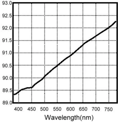
Fig. 3-2 The transmittance of conventional buffer layer within visual light range of human.---44
xv
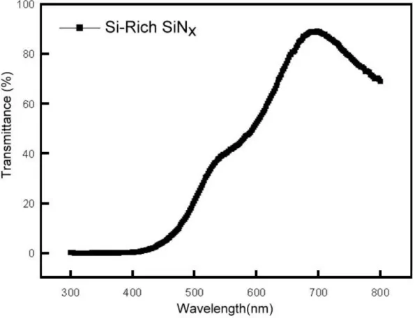
Fig. 3-3 The transmittance of Si-rich SiNX buffer layer as the wavelength sis varied
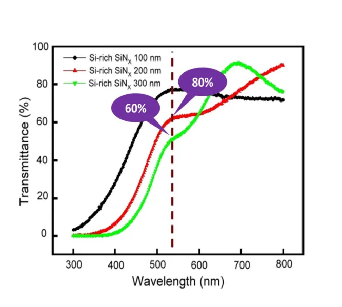
from 300nm to 800nm.---45 Fig. 3-4 The comparison in transmittance of Si-rich SiNX buffer layer as the film
thickness is 100nm, 200nm and 300nm.---46 Fig. 3-5 (a)The results of photo leakage current in poly-Si TFT with conventional
buffer layer, Si-rich oxide buffer layer and Si-rich SiNX buffer layer as VD
is -0.1V. (b)The results of photo leakage current in poly-Si TFT with conventional buffer layer, Si-rich oxide buffer layer and Si-rich SiNX
buffer layer as VD is -9v.---47
Fig. 3-6 The comparison of variation in sub-threshold swing of poly-Si TFT with conventional buffer layer, Si-rich oxide buffer layer and Si-rich SiNX
buffer layer under illumination as VD is -0.1v.---48
Fig. 3-7 The proposed process diagram for treating the surface of buffer layer using NH3 plasma bombardment. Numerous state densities are generated to be
taken as the recombination center for light-induced electron-hole pairs.--49 Fig. 3-8 The comparison of electrical characteristics in conventional and proposed
poly-Si TFT under dark state.---50 Fig. 3-9 As the brightness of back-light is set as 2160, 3100, 4110 and 5620 nit, the
comparison in photo leakage current of conventional and proposed devices. The remarkable reduction of photo leakage current in proposed TFT is observed.---51 Fig. 3-10 As the brightness of back-light is set as 2160, 3100, 4110 and 5620 nit, the
sub-threshold swing of conventional and proposed devices. As the brightness of back-light is 5610 nit, the maximum ΔS.S of conventional and proposed TFT are 46.4% and 85.3%---52
xvi
Chapter 4:
Fig. 4-1 The key process diagram for treating the surface of buffer layer using Ar ion implant bombardment. Numerous state densities are generated to be used as the recombination center for light-induced electron-hole pairs.---63 Fig. 4-2 The proposed poly-Si TFT with patterned metal shielding layer. The width of exposure region is 3μm.---64 Fig. 4-3 ID-VG curves of the conventional poly-Si TFT operated in the linear region
under illumination and dark states. A significantly increase in leakage current and sub-threshold swing was observed.---65 Fig. 4-4 The ID-VG characteristics in treated TFTs under dark state and photo
state.---66 Fig. 4-5 Explanation of current flow of poly-Si under illumination.---67 Fig.4-6 ID-VG characteristics of proposed TFT operated with low and high drain
voltage in forward and reverse modes at dark.---68 Fig. 4-7 ID-VG curves of poly-Si TFT in forward measurement as drain bias is 0.1V
and 9V. A high photo leakage current and almost unchanged sub-threshold swing are observed.---69 Fig. 4-8 ID-VG curves of poly-Si TFT in reverse measurement as drain bias is 0.1V
and 9V. With the low drain bias, the photo leakage current is lower than that in forward mode and the sub-threshold swing is also nearly unchanged. However, S.S is degraded markedly with high drain voltage.---70 Fig. 4-9 The diagrams of proposed model for electrical characteristics of poly-Si
TFT with patterned metal shielding layer under back light in forward and reverse modes, respectively.---71 Fig. 4-10 Proposed band diagram to explain the degradation of sub-threshold swing in
xvii
Chapter 5:
Fig. 5-1 The stress pulses were conducted on the gate electrode as the dynamic stress and source/drain were grounded. The rectangular pulse with amplifier of ±15V and frequency of 500kHz. Both the rising time (Tr) and falling time (Tf) were 100 ns.---82 Fig. 5-2 The ID-VG relationships of n-channel poly-Si TFT (L=9μm) with the
dynamic stress times for 10 to 1000 seconds.---83 Fig. 5-3 The ID-VD characteristics of the TFT with the dynamic stress times.---84
Fig. 5-4 The initial CGD of n-channel poly-Si TFTs curves at the different
measurement frequency.---85 Fig. 5-5 C–V curves of an n-channel TFT after dynamic stress for 1000s. (a)
Gate-to-drain capacitance. (b) Gate-to-source capacitance.---86 Fig. 5-6 C–V curves of an n-channel TFT after dynamic stress. (a) Gate-to-drain
capacitance at 10 kHz. (b) Gate-to-drain capacitance at 1MHz.---87 Fig. 5-7 The process flow of two shot SLS crystallization technology.---88 Fig. 5-8 (a) The top view of a high-resolution scanning electron microscopy (SEM) image of laser-crystallized laterally grown poly-Si film. (c) The orientation of main-GB and sub-GB is perpendicular and parallel to channel direction of the TFTs we utilized, respectively. (b) The AFM image of laser-crystallized laterally grown poly-Si film.---89 Fig. 5-9 The ID-VG curves of NGB and GB TFTs under the dynamic stress times for
10 to 1000 s. The degradation in GB TFTs is more severe.---90 Fig. 5-10 The C–V curves of NGB and GB TFTs. It is shows that the gate oxide
capacitance in GB TFTs is higher than the one in NGB TFTs.---91 Fig. 5-11 The simulation result of the electric filed distribution in the protrusion
xviii
Fig.5-12 The degradation model which considers the effect of protrusion grain boundaries as TFTs is operated under dynamic stress.---93
Chapter 6:
Fig. 6-1 The distribution of the threshold voltage among 600 TFTs and the maximum shift of the threshold voltage are about 0.2V.---106 Fig. 6-2 Circuit scheme of conventional pixel circuit (2T1C) and the voltage drop
caused by the intrinsic parasitic resistance (R) at Vdd supply power line.---107 Fig. 6-3 The proposed pixel design and timing scheme of the signal line.---108 Fig. 6-4 The equivalent circuit at each stage in operation.---109 Fig. 6-5 The transient simulation results for the conventional 2T1C pixel structure
with the variation in the threshold voltage of DTFT.---110 Fig. 6-6 The gate voltage stored in the capacitor with varied threshold voltages of
DTFT.---111 Fig. 6-7 (a) The transient simulation results for the proposed pixel structure. With
the threshold voltage shift of DTFT set as 0.3V, the variation of output current is about 1.01~0.99 μA. (b) The transient simulation results for the proposed pixel structure. The deviation of IOLED in the proposed pixel
structure is less than 2.5% in the degradation of the supply voltage on panel is 0.5V.---112 Fig. 6-8 Comparison of non-uniformity of output current between the conventional
pixel structure (2T1C) and the proposed one (5T1C), caused by the drop in supply voltage with increasing number of scan lines (240, 480, 600, 768).---113
xix
Fig. 6-9 Error rate of output current in our proposed pixel circuit due to the threshold voltage variation. The error rate of output current with the proposed design is all less than 2.5% as input data voltage ranges 1–5
V.---114
Fig. 6-10 The proposed pixel design and its timing scheme of the signal line.---115
Fig. 6-11 The equivalent circuit at each stage in operation.---116
Fig. 6-12 The transient simulation result of proposed pixel design.---117
Fig. 6-13 (a) Simulation result of the conventional 2T1C pixel circuit. The variation range of IOLED in 2T1C pixel is about 1.04 to 0.68 μA. (b) Simulation result of the conventional 2T1C pixel circuit as the threshold voltage shift in DTFT is set to 1.2V.---118
Fig. 6-14 (a) Simulation result of the conventional 2T1C pixel circuit. The degradation of IOLED in 2T1C pixel is about 1.04 to 0.76 μA. (b) Simulation result of the conventional 2T1C pixel circuit as the threshold voltage in OLED is set to 0.7V.---119
Fig. 6-15 The simulation result of driving current of proposed pixel circuit with increasing threshold voltage shift.---120
Fig. 6-16 Threshold voltage shift versus stress time. The straight lines are from the plots of threshold voltage shift against stress duration.---121
Fig. 6-17 The simulated result about the lifetime of 2T1C and proposed pixel. Considering the degradation of TFT and OLED with time, the proposed circuit exhibits only 10% current degradation at 5000H.---122
1
Chapter 1
Introduction
1.1 General Background
Thin film transistor (TFT) is a metal-oxide-silicon field effect transistor (MOSFET) fabricated on an insulator substrate by employing all thin film constituents. Thin film transistors have been widely used as switching devices in flat panel display, such as active-matrix liquid crystal display (AMLCD) [1.1-1.5] and active-matrix organic light emitting diode (AMOLED) display [1.6-1.10]. The active layers of thin film transistors can be mainly divided into two types, amorphous silicon (a-Si) and poly-crystalline silicon (poly-Si), according to the crystallization status. The hydrogenated a-Si (a-Si:H) TFT is commonly applied in large size active matrix displays (AMDS) due to its highly mature process, low manufacturing cost and good device uniformity. However, the threshold voltage of a-Si:H TFT would increase with long time operation. Therefore, the poor stability limits the application of a-Si TFT in AMDs. On the contrary, poly-Si TFT is suitable for the high-resolution, compact size active matrix display in mobile electrical products. Since mobility and stability of poly-Si TFT is higher than a-Si TFT, it offers a promising solution to realize the “System on Panel” technology. The high driving capability and existence of complementary devices lead to integrate functional and driver circuits on the glass substrate. The improvement of electrical characteristics and understanding of degraded mechanism of poly-Si TFTs is important for development of advanced mobile display technology. In addition, AMLCD requires back-light source to display
2
input image. However, poly-Si TFT operated in illumination environment exhibits an undesired high leakage current to affect the function of pixel switch [1.11].
Furthermore, AMOLED technology with high brightness, high color saturation and fast response time has attracted more and more attention worldwide. Since the brightness of OLED is strongly dependent of driving current, it needs a well-controlled current source to provide the uniform brightness among numerous pixels. Since the main backplane technologies of AMLCD, a-Si TFT and ploy-Si TFT have been developed in the past 20 years, they can be directly taken as the pixel switch and the driving current source for AMOLED. Using excimer laser to re-crystalline a-Si active layer, poly-Si TFT can offer very high current capability. However, the laser re-crystallization process also generates plenty of the grain boundaries in poly-Si TFT, leading to poor uniformity and very huge variation due to the narrow laser process windows for producing large grain size poly-Si TFT. The fluctuation of pulse-to-pulse laser energy and non-uniform laser beam profile make laser energy density hard to hit the super lateral regime everywhere. The random grain boundaries and traps exist in the channel region [1.12-1.14]. This will cause serious non-uniformity of brightness in AMOLED panel. Since the device-to-device uniformity is hard to control, it is essential to develop circuits to compensate the variation. Another one of promising approaching for AMOLED backplane is to use a-Si TFT because of its many advantages, including simple manufacturing process low-cost in large size panel and good device uniformity. However, it had been reported that the threshold voltage of a-Si TFT would shift during operation with increasing time [1.15-1.16]. The increasing threshold voltage of a-Si TFT would reduce the current driving capability to result in the lower brightness of OLED after long time operation. In addition, the threshold voltage of OLED is also shifted with
3
time. Therefore, the current originated from a-Si TFT would be very sensitive to the OLED degradation.
1.2 Motivation
Hydrogenated amorphous silicon (a-Si:H) technology is quite attractive in AMDs due to its low processing temperature and low manufacture cost. The bottom gate inverted-staggered back-channel-etched (BCE) type of a-Si:H TFT shown in Fig 1.1 has been widely used as a switching element to control the gray level in AMLCD and to drive AMOLED. AMLCD panels are usually used in an illumination environment such as under the back-light. Therefore, the leakage current of TFT under back-light illumination in TFT-LCD displays should be reduced to avoid losing the storage charges in the pixel. Although photo leakage current of inverted staggered a-Si:H TFT was also a serious problem, it had been solved by light-shielding structure proposed by Akiyama et al.
Compared with a-Si:H TFT technology, the poly-Si TFT technology has some distinct advantages but its manufacture is more complex and high cost. The major advantage of poly-Si TFT is the higher field effective mobility than that of the amorphous silicon (a-Si) based devices. The high carrier mobility and the existence of complementary pairs permit the integration of drive circuits and the smaller area of pixel transistor. The integration of drive circuits could reduce manufacturing costs, and increase the functionality of large-area microelectronics [1.17-1.18]. The smaller area of pixel transistor leads to a larger aperture ratio for a given pixel size, or enables a high resolution display for a given aperture ratio, resulting in fine image quality for mobile display. Recently, the demand of high-end mobile electronic products such as
4
cell phone, digital camera, GPS, mobile TV and so on is continuing to grow, so that the development of mobile displays with high resolution and high image quality is inevitable. Since most of people would like to use mobile electronic products outdoors under the sunlight, the readability in ambient illumination is a critical issue for mobile displays. To meet the requirement of superior readability under sunlight, the brightness of backlight becomes higher and higher. However, poly-Si TFTs operated in the high illumination environment exhibit substantial photo leakage current and degraded sub-threshold-swing (S.S), leading to the errors of gray level and difficulty in pixel design.
In addition, the application of circuit integration using poly-Si TFT continuously grow up as device characteristics improve further. Enlarging the grains in poly-silicon layers is an effective approach for improving TFT performance. Several poly-Si re-crystallization methods based on laterally grown grains have been proposed to enlarge the grains and control the location of the grain boundaries [1.19-1.20]. In poly-Si TFT devices, however, the status of defect states at grain boundaries plays a crucial role for electrical characteristics, as shown in Fig. 1.2 and Fig. 1.3. The stability of poly-Si TFT is one of the important issues for poly-Si technology. Recently, the researches about the stabilities of conventional excimer laser-crystallized (ELC) poly-Si TFTs have been reported. The creation of trap states at poly-Si/gate dielectric interface or the charge trapping in the gate insulator is responsible for the degradation in electrical characteristics of poly-Si TFTs. Since TFT devices in driving circuits are frequently subjected to high-frequency voltage pulses, the degradation behavior under dynamic stress is a critical issue for integrated peripheral circuits.
5
efficiency, fast response time and wide viewing angle. Although poly-Si TFT is considered as the main backplane technology for AMOLED, the device variation is still a most critical issue to implant AMOLED panel with good image quality. The conventional 2T1C pixel shown in Fig. 1.4 directly suffers from the non-uniformity of brightness among pixels. For the demand of large size AMOLED panel, this problem will become more and more serious. To solve this issue, several methods have been proposed to compensate for the variation in poly-Si TFT characteristics. The pixel circuit of AMOLED displays can be divided into two catalogs, including voltage driving and current driving methods [1-21-1.22]. The current driving method can provide an excellent uniformity of brightness. However, it need a long time to driving panel for high resolution displays. The voltage driving method can compensate for the variation of the threshold voltage and is easy to integrate poly-Si TFT drivers on the glass substrate. Therefore, the voltage driving method would be considered as a great potential solution for eliminate the variation of poly-Si devices.
In addition, recently, a-Si:H TFT attract much attention to be taken as pixel element for large size and low cost panels in AMOLED display because of its good uniformity and simple fabrication process [1.23-1.24]. However, the threshold voltage shift of a-Si:H TFT over time under operation is another critical issue to degrade the image quality on AMOLED panels [1.25]. Moreover, since OLED is placed on the source node of a-Si:H TFT in the conventional pixel circuit and IOLED is determined by VGS of
the driving TFT, the threshold voltage shift in OLED raise the source voltage of the driving TFT to decrease the driving current..
In this thesis, the electrical characteristics of poly-Si under illumination are studied in detail. In order to solve the photo leakage current problem, a metal shielding layer structure for poly-Si TFT is used for top gate poly-Si TFT structure. From the SEM
6
image and transfer curves of poly-Si TFT with metal shielding layer, the elimination of photo leakage current and increase in S.S are confirmed. However, VTH of poly-Si
TFT with metal shielding layer would shift with the drain bias. Therefore, a simple method to improve the electrical characteristics of poly-Si TFT under illumination and maintain the original key parameters is proposed. In addition, the behavior of S.S under illumination is also discussed based on the result of proposed test devices. An energy band diagram is proposed to explain the degradation of S.S under light exposure. Furthermore, the mechanism of conventional ELC poly-Si TFT under dynamic stress is investigated by voltage-capacitance measurement. We also proposed a model to describe the degradation of laser-crystallized laterally grown poly-Si under dynamic stress. For the application of poly-Si TFT in AMOLED, a 5T1C design is proposed to eliminate the VTH variation of poly-Si TFT and the voltage drop of supply
power in one time operation. Additionally, a simple pixel circuit composed of 4T1C with source follower type compensation is presented to release the issue of degradation in a-Si TFT and OLED.
1.3 Thesis Organization
In this thesis, novel methods to lower the leakage current and improve the sub-threshold swing of low-temperature polycrystalline silicon thin film transistors (poly-Si TFT) under illumination were proposed. Furthermore, the models of electrical characteristics of poly-Si TFT under illumination were investigated and established in detail. In addition, the new compensation pixel circuits and driving schemes for AMOLED employing poly-Si TFT and a-Si:H TFT were developed in this work. The dissertation is organized in to the following chapters:
7
In chapter 1, a brief overview of TFT technology and the pixel circuit for AMOLED displays are introduced. We describe the trend and issues of poly-Si TFT development and the problems of TFT applied for the element device of AMOLED pixel circuits. Then, the outline throughout the dissertation is discussed here.
In chapter 2, a new structure of top gate poly-Si TFT to eliminate the photo leakage was first proposed. By this structure, the photo leakage and degradation of sub-threshold swing in poly-Si TFT under illumination are totally eliminated. However, the threshold voltage of device with this structure would shift as drain bias is increasing. Therefore, a modified shielding structure of poly-Si TFT with low photo leakage current is developed to release this issue.
In chapter 3, the buffer layer is modified to improve the electrical characteristics of poly-Si TFT under illumination. A Si-rich dielectric film is taken as the buffer layer to absorb the backlight. Therefore, the light absorbed by poly-Si layer is reduced to lower photo leakage current and sun-threshold swing. Furthermore, the state densities in the interface of poly-Si film and buffer layer are induced by NH3 plasma treatment
on the surface of buffer layer. The light-excited electrons and holes would recombine directly via the extra state densities. The fewer excess electron-hole pairs lead to the less photo leakage current and sub-threshold swing.
In chapter 4, the mechanism of photo leakage current and the increase of sub-threshold swing in poly-Si TFT under illumination are studied in detail. By the results of treated poly-Si TFT, the excess electron-hole pairs in the bottom of poly-Si film are the main factor to influence the electrical characteristics of device operated in the backlight environment. Furthermore, the patterned metal shielding layer is used to control the light exposure region in the source or drain junction. Based on the experimental results, the effective factors to degrade the sub-threshold swing and raise
8
the photo leakage current are verified.
In chapter 5, the AC stress effect of poly-Si TFT with excimer laser crystallization (ELC) and laser-crystallized laterally grown grain is studied. The generated tail state densities in the source and drain junction in confirmed by capacitance-voltage (C-V) measurement. In addition, the grain boundary effect in reliability of poly-Si TFT under AC stress is investigated.
In chapter 6, a novel poly-Si TFT pixel circuit and driving scheme is proposed. It is composed of five poly-Si TFT and one capacitor. The control line is two lines, including [n]scan and [n]EM. The function of this design is verified by simulation work using HSPICE software. Furthermore,a simple pixel a-Si:H TFT circuit and driving scheme is proposed. It is composed of five a-Si:H TFT and one capacitor to compensate for the shift in the threshold voltage of driving TFT and OLED at one time operation. The function of this design is verified by simulation work using HSPICE software.
9
10
Figure 1-2 (a) Model for the crystal structure of polysilicon films. (b) The charge distribution within the crystallite and at the grain boundary. (c) The energy band structure of the polysilicon crystallites
11
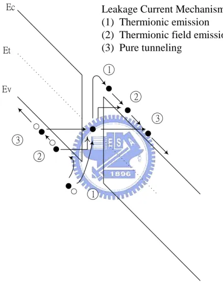
Fig. 1-3 Three possible mechanisms of leakage current in poly-Si TFTs, including thermionic emission, thermionic field emission and pure tunneling.
1 2 3 2 1 3 Ec Ev Et
Leakage Current Mechanism
(1) Thermionic emission
(2) Thermionic field emission
(3) Pure tunneling
12
Fig. 1-4 Diagram of conventional 2T1C pixel structure for AMOLED displays
Scan line
D
a
ta
l
in
e
DTFT
TFT1
C
ST
VDD
OLED
13
Chapter 2
Polycrystalline Thin Film Transistor with Metal Shielding Layer
2.1 Introduction
Low-temperature polycrystalline-silicon thin film transistors (poly-Si TFTs) have been widely investigated for flat-panel applications such as active matrix liquid crystal display (AMLCD) and active matrix organic light-emitting diode display (AMOLED) [2.1-2.3]. Recently, the demand of high-end mobile electronic products such as cell phone, digital camera, GPS, mobile TV and so on is continuing to grow rapidly, so that the development of mobile displays with high resolution and high image quality is inevitable. Since most of people would like to use high-end mobile electronic products outdoors under the sunlight, the readability in ambient illumination is a critical issue for mobile displays [2.4-2.5]. To meet the requirement of superior readability under sunlight, the brightness of backlight becomes higher and higher. However, poly-Si TFTs operated in the high illumination environment exhibit substantial photo leakage current (IPLC). The leakage current of TFT under back-light
illumination in AMLCD displays should be reduced to avoid losing the storage charges in the pixel. Therefore, the voltages that are held across the pixel electrodes would be diminished to affect the gray level controlling, which in turn, would cause a low contrast ratio and error color display. Although IPLC of inverted staggered a-Si:H
TFT was also a serious problem, it had been solved by light-shielding structure proposed by Akiyama et al [2.6]. Since the gate metal is normally under a-Si:H layer for inverted staggered structure, the light-shielding structure can be performed easily
14
by patterning a-Si:H layer to be located totally inside the gate metal. Figure 2.1(a) shows the conventional poly-Si TFT structure. It is a top gate structure, indicating the gate metal is on the top of active layer, so that light form back-light directly emit into poly-Si film to be absorbed, generating IPLC and increasing sub-threshold swing (S.S).
However, the studies for lowering IPLC in poly-Si TFTs with top gate structure are
very few [2.7-2.8].
In this chapter, we propose a new light-shielding structure for poly-Si TFT with top gate to eliminate the IPLC originated from the illumination of back-light. The IPLC and
the S.S variation of proposed TFTs are entirely cancelled by the light-shielding layer. In addition, the electrical characteristics of poly-Si TFTs with light-shielding layer are investigated first. As drain bias changes, the shift of threshold voltage (VTH) of
poly-Si TFT with metal shielding layer is observed, inducing the un-saturation phenomenon of ID-VD characteristics. Therefore, the VTH of poly-Si TFT is affected by
the insert metal shielding layer. In order to solve the variation of VTH with drain bias,
the metal shielding layer is patterned to be partially under poly-Si layer. The location of partial metal shielding layer is designed to be channel or close to junction region. The relationship between location of partial metal shielding layer and effect of lowering IPLC is discussed as device is operated in linear and saturation regions.
2.2 Full Metal Shielding Layer Structure
2.2.1 Experimental Procedure
The poly-Si TFTs with top gate p-channel and lightly doped drain (LDD) structure were fabricated on Corning1737 glass substrate. First of all, an 80nm thick molybdenum film was sputtered to be a shielding layer on the glass substrate. The buffer layer and a thin 50 nm-thick un-doped amorphous-Si (a-Si) film were
15
sequentially deposited by plasma enhanced chemical vapor deposition (PECVD) at 380℃, followed by dehydrogenated via furnace annealing process at 450℃. Then the a-Si films were crystallized by 308nm XeCl excimer laser with the line-shaped beam power of 350mJ/cm2. The active island, the buffer and the light-shielding layers were patterned using the same mask by plasma dry etching. The 100nm thickness gate insulator was deposited by tetraethyl orthosilicate base (TEOS) oxide. The source/drain regions were defined by a mask and formed by the mass-separated ion implanter technique. Then, MoW was sputtered and patterned as a gate metal. Following, implantation for LDD region is preformed on overall device after the S/D photo resistor is removed. The doping activation was performed by RTA irradiation. The dimensions of TFTs in this work were L = 6 μm, W = 6 μm and the LDD length is 1.25 μm. The brightness of back-light for photo state measurement is set as 3000nits. In the manufacture process, the number of masks is equal to the conventional poly-Si TFT procedure.
2.2.2 Results and Discussion
The cross-sectional view of proposed TFT is illustrated in Fig. 2.1(b). A thin metal film is deposited on the glass substrate to block the light emitted into poly-Si thin film. For the AMLCD application, most pixel regions should be allowed light to pass through so that the metal shielding layer must be patterned to be an opaque area only for the poly-Si active island. To simplify the manufacture process, the metal shielding layer, buffer layer and active island layer are patterned in the same mask employing plasma dry etching process. Therefore, the process of the proposed structure is compatible with conventional one. Figure 2.2 shows the SEM image of poly-Si TFT
16
with the light-shielding layer. After one time etching process, the triple layers, including metal film, buffer oxide and poly-Si film, show a taper-like shape and the area of metal layer is larger than that of the active layer. Since the poly-Si island is completely located inside the coverage of metal shielding layer, the result confirms that the proposed device exhibits a strong immunity to high brightness illumination.
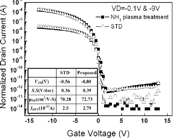
Figure 2.3 shows the ID-VG transfer curves of standard poly-Si TFT at the linear
operation under the dark and photo states. The leakage current of poly-Si TFTs in the dark was around 10-13 A as the gate bias is varied from 0 to -12 V. With the same range of gate bias, the leakage current of poly-Si TFTs under illumination is as high as two orders of magnitude, about 10-11A. It is clearly observed that the on/off current ratio of poly-Si TFTs was substantially decreased to seriously affect the function of TFTs used as the pixel switch under illumination environment. In addition, the sub-threshold swing is increased under illumination, about 0.49 V/decade, as the initial value in dark is 0.28 V/decade. The variation of sub-threshold swing is about 75%. Since the light from back-light is mainly absorbed at the interface of poly-Si and the glass substrate, plenty of light-induced electron-hole pairs are accumulated in the bottom of poly-Si film to generate the IPLC [2.9].
To solve this issue, the poly-Si TFT with full metal shielding structure was proposed. The ID-VG transfer curves of proposed poly-Si TFT under the dark and
photo states are shown in Fig. 2.4. It is clearly observed that the IPLC is entirely
eliminated in the proposed poly-Si TFT and the shielding effect is independent of drain bias. The leakage current is about 10-13 A under illumination at the linear operation, as same as that in the dark state. The sub-threshold slope is also unchanged absolutely under illumination by the light-shielding structure. Figure 2.5(a) plots the ID-VG curves of the poly-Si TFT with increasing drain bias under dark. As the drain
17
voltages are -4.5V and -9V, the negative shifts of VTH are 1.08V and 2.07V,
respectively. It indicates that the proposed TFTs are easier to be turned on by the high drain voltage. However, the VTH of conventional poly-Si TFT slightly shifts under
high drain voltage operation at dark and photo states. In addition, from the result shown in Fig. 2.5(b), the un-saturation phenomenon of ID-VD of poly-Si TFT with full
metal shielding layer is found clearly. The VTH of proposed TFT is dependent of drain
voltage so that the drain current would increase with drain bias.
Since the metal film is located under the poly-Si active layer, a parasitic capacitance in the overlap of source and drain side is generated. The negative voltage at drain side would lead to a negative potential distribution, VM, in the metal film
owing to the coupling effect. VM is regarded as the substrate bias to affect the
threshold voltage of the proposed poly-Si TFTs [2.10]. Therefore, the threshold voltage shifts in positive are explained by the negative VM coupled from the applied
drain bias. In practical application of TFT-LCD, the range of gate voltage applied to pixel switch is from -10V to 6 V for p-channel device and the input range of data signal is from 0V to 5V. It means that the TFT used as pixel switch is operated at the linear region. Considering the advantages of proposed TFT such as high on/off ratio and unchanged sub-threshold swing due to the elimination of IPLC under illumination,
the slight shift of threshold voltage is acceptable. However, poly-Si TFT is taken not only as switch device in pixel but also component for integration of peripheral driving circuits. The shift in VTH with drain voltage is a rather serious issue for circuits design.
Therefore, the partial metal shielding structure for poly-Si TFT is proposed and discussed in the next section.
18
2.3 Partial Metal Shielding Layer Structure
2.3.1 Experimental Procedure
The n-channel poly-Si TFTs with LDD structure were fabricated on Corning1737 glass substrate. First of all, a 50nm thick molybdenum film was sputtered and was patterned using additional mask to be a shielding layer on the glass substrate. The buffer layer and a thin 50 nm-thick undoped a-Si film were sequentially deposited by PECVD at 380℃, followed by dehydrogenated via furnace annealing process at 450 ℃. Then the a-Si films were crystallized by 308nm XeCl excimer laser with the line-shaped beam power of 350mJ/cm2. The 100nm thickness gate insulator was deposited by TEOS oxide. The source/drain regions were defined by a mask and formed by the mass-separated ion implanter technique. Then, MoW was sputtered and patterned as a gate metal. Following, implantation for LDD region is preformed on overall device after the S/D photo resistor is removed. The doping activation was performed by RTA irradiation. The dimensions of TFTs in this work were L = 18 μm, W = 18 μm and the LDD length is 1.25 μm.
2.3.2 Results and Discussion
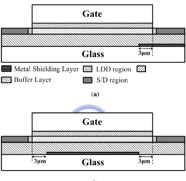
The partial metal shielding layer is located junction in and channel region as shown in Fig.2.6(a) and 2.6(b), respectively. As the shielding metal is located in the channel and shorter than the gate metal shown in Fig. 2.6(b), the space between the edge of shielding metal and the gate metal is set to 3μm. Figure 2.6(a) plots the poly-Si TFT with shielding metal remained to be located in junction side. Similarly, the overlap region between the edge of shielding metal and the gate metal is 3μm. Therefore, the
19
effect of location for IPLC is investigated employing the two types of poly-Si TFT with
different partial metal shielding structure.
Figure 2.7 plots the ID-VG relationships of poly-Si TFT with partial metal shielding
layer located in channel region (Channel-shielding TFT) and drain junction region (Drain-shielding TFT) as drain voltage is varied at dark state. It is clearly found that the VTH of poly-Si TFT with partial metal shielding layer is independent of drain bias
and the location of shielding metal. As shielding metal is located in junction region, the parasitic capacitance is performed in the overlap region between drain side and shielding metal. However, the floating potential, VM, induced by drain voltage is
distributed in the shielding metal region located only in drain side. The channel region would not be affected by VM to induce the back channel in the bottom of poly-Si layer.
Therefore, VTH of Drain-shielding TFT is unchanged with increasing drain bias. By
contrast, the shielding metal is completely located inside the coverage of gate metal so that the parasitic capacitance originated from overlap region between shielding metal and drain side is vanished. Therefore, the increasing drain voltage of Channel-shielding TFT could not induce VM to attribute to the shift of VTH.
Figure 2.8(a) reveals the comparison of IPLC which is extracted at a voltage
|VG-VTH| of 7V as VD is 0.1V for TFT with partial metal shielding layer located in
channel region (Channel-shielding TFT), drain side (Drain-shielding TFT) and source side (Source-shielding TFT) as brightness of back-light is in Channel creased (2160, 3100, 4110, 5620 nits). The IPLC of Drain-shielding TFT is much lower than that of
Channel-shielding TFT and Source-shielding TFT. The maximum values of IPLC of
Drain-shielding TFT, Channel-shielding TFT and Source-shielding TFT are 4.1, 19.2 and 24.5 pA. In addition, the IPLC of Drain-shielding TFT exhibits a weak dependence
20
dominant region for IPLC of poly-Si TFT operated in linear region. Figure 2.8(b)
shows the IPLC of Drain-shielding TFT, Channel-shielding TFT and Source-shielding
TFT as drain voltage is 9V. It is observed the shielding effect of Drain-shielding TFT is reduced markedly even if the IPLC of Drain-shielding TFT is still less than that of
Channel-shielding TFT and Source-shielding TFT.
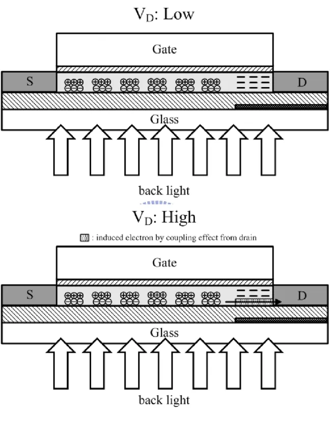
While poly-Si TFT is exposure to back-light, the excess electron-hole pairs are generated. The regions generating photo-induced electron-hole pairs can be divided into two parts. One is drain junction region and another is channel region. The excess electron-hole pairs generated in drain junction would be separated due to the electric field and the excess electrons could flow to drain to become leakage current. By contrast, since Si is an indirect band gap material, photo-induced electron-hole pairs in channel region could not be recombined directly. Therefore, the excess electrons in channel region would diffuse to drain to form current. It is inferred that the IPLC is
attributed to the diffusion current and drift current from channel region and drain junction, respectively. As shown in Fig. 2.9, the band diagram to explain the generation of IPLC for Source-shielding TFT is proposed. Since the shielding metal is
located in source side, the excess electrons generated at channel and junction region flow to drain by diffusion and drift, leading to the high IPLC. Figure 2.10 shows the
band diagram of Drain-shielding TFT under illumination. As the shielding metal is located in drain side, light emitting to the junction region is blocked to eliminate the junction part of IPLC. In addition, the electrons induced by light outside the shielding
metal are difficult to diffuse to drain since the excess electrons must to pass through an intrinsic poly-Si region, while drain voltage is 0.1V. Hence, Drain-shielding TFT operated in linear region exhibits a highest immunity to illumination environment compared to Source-shielding TFT and Channel-shielding TFT. However, as the high
21
voltage is applied at drain, a positive potential distribution, VM, in the shielding metal
of Drain-shielding TFT owing to the coupling effect is generated due to the parasitic capacitance in the overlap of drain and shielding metal. Hence, electrons induced by VM gather to form the back channel near drain in the bottom of poly-Si layer, as
illustrated in Fig. 2.11. So that excess electrons at channel region would flow to drain through the back channel under high drain bias, generating IPLC. Therefore, the
shielding effect of Drain-shielding TFT under illumination would be suppressed by applied high drain voltage.
2.4 Conclusions
We have demonstrated a new and simple method to fabricate the top gate poly-Si TFT with the light-shielding structure first. The proposed full metal shielding TFT is free of photo leakage current under illumination for high image quality AMLCD application. The process of the proposed structure without adding the number of masks is compatible with the conventional poly-Si TFTs. In addition, the shift in threshold voltage of the proposed TFTs with the increasing drain bias in dark state is explained by the coupling effect. In order to overcome this issue and investigate the generation mechanism of IPLC, poly-Si TFT with the partial shielding metal located in
junction and channel region is fabricated. It is shown that VTH of poly-Si TFT with
partial metal shielding layer is independent of increasing drain bias. Furthermore, the Drain-shielding TFT exhibits impressively low IPLC and the shielding effect of the
Source-shielding TFT and Channel-shielding TFT are rather poor. The IPLC of
Drain-shielding TFT, Channel-shielding TFT and Source-shielding TFT are 4.1, 19.2 and 24.5 pA as brightness of back-light is 5610 nits. From the comparison of IPLC of
22
Drain-shielding TFT, Source-shielding TFT and Channel-shielding TFT, the band diagram of poly-Si TFT under illumination is proposed. In addition, the shielding effect of Drain-shielding TFT would be suppressed as the high drain voltage.
23
Fig. 2-1 (a) Conventional top gate structure of poly-Si TFT. (b) The new structure of proposed Poly-Si TFT. A metal film is located under the active island to be a light-shielding layer.
24
Fig. 2-2 The SEM image of metal shielding layer, buffer layer and Poly-Si layer after etching process using the same mask.
25
Fig. 2-3 ID-VG curves of the conventional poly-Si TFT operated in the linear region
under illumination and dark states. A significantly increase of leakage current was found.
26
Fig. 2-4 ID-VG curves of proposed Poly-Si TFT under illumination and dark states.
The photo leakage current and the variation of sub-threshold swing under illumination are eliminated entirely.
27
Fig. 2-5 (a) ID-VG curves of proposed Poly-Si TFT as VD is set as -0.1, -4.5 and -9V. It
is found that the threshold voltage shifts with the increasing drain voltage. (b) ID-VD
curves of Poly-Si TFT with full metal shielding layer as VG is varied. It shows that the
drain current is strongly dependent of the applied drain voltage.
(a)
-15 -12 -9 -6 -3 0 0.0 5.0x10⁻⁵ 1.0x10⁻⁴ 1.5x10⁻⁴ 2.0x10⁻⁴ 2.5x10⁻⁴D
ra
in
C
u
rr
e
n
t (A
)
Drain Voltage
VG= -3V VG= -6V VG= -9V VG= -12V VG= -15V(b)
28
Fig. 2-6 (a) Proposed Poly-Si TFT with partial metal shielding layer which is located in the junction region. (b) Proposed Poly-Si TFT with partial metal shielding layer which is located in the central channel region.
(a)
29
Fig. 2-7 the transfer curves of poly-Si TFT with partial metal shielding layer located in channel region (Channel-shielding TFT) and drain junction region (Drain-shielding TFT) as drain voltage is varied at dark state.
-15 -10 -5 0 5 10 15 10-14 10-13 10-12 10-11 10-10 10-9 10-8 10-7 10-6 10-5 10-4 10-3 VD= 0.1V V D= 5V V D= 9V