IEEE ELECTRON DEVICE LETTERS, VOL. 33, NO. 3, MARCH 2012 393
Three-Transistor AMOLED Pixel Circuit With
Threshold Voltage Compensation Function
Using Dual-Gate IGZO TFT
Ya-Hsiang Tai, Lu-Sheng Chou, Hao-Lin Chiu, and Bo-Cheng Chen
Abstract—In addition to the gate electrode at the bottom, a dual-gate amorphous InGaZnO4 thin-film transistor (TFT) has a secondary gate electrode on the top. The threshold voltage (Vth) of the TFT using the bottom gate in its normal operation can be controlled by the top gate. Based on this phenomenon, a simple circuit of active-matrix organic light-emitting diode using the top gate to compensate threshold voltage variation is proposed. This new pixel circuit uses only three TFTs and two capacitors. The validity of Vth compensation is verified experimentally.
Index Terms—Active-matrix organic light-emitting diode (AMOLED), dual-gate amorphous InGaZnO4 (a-IGZO) thin-film transistor (TFT), threshold voltage (Vth) compensation circuit.
I. INTRODUCTION
M
ANY pixel circuits of active-matrix organic light-emitting diode (AMOLED) were proposed to compen-sate the threshold voltage (Vth) of the thin-film transistor (TFT) for the good display quality since the Vth shift issue in the AMOLED circuit is very critical [1], [2]. Usually, it takes many TFTs to implement the circuit, which can lower the aperture of the display pixel [3]–[9]. To make the aperture large while keeping the Vth compensation function, several pixel circuits composed of fewer transistors were proposed [10]– [15]. However, some of the published circuits have drawbacks such as the current driving scheme [12], the need of both n-and p-type TFTs [13], individual driving of the anode n-and the cathode of OLED [14], or indirect voltage driving through capacitive coupling[15]. Taking the advantage of the fact that the Vth of dual-gate amorphous InGaZnO4 (a-IGZO) TFT can be controlled by the second gate of the TFT [16], [17], Jankovic and Brajovic proposed a pixel circuit [18], but it is based on a premise that the effect of the second gate on the Vth of the dual-gate TFT is constant, which is not necessarily true.Manuscript received November 8, 2011; accepted December 3, 2011. Date of publication January 10, 2012; date of current version February 23, 2012. This work was supported by the National Science Council of the Republic of China under NSC100-2628-E-009-021-MY3 and Frontier Photonics Research Center of the Republic of China under 100W959. The review of this letter was arranged by Editor A. Nathan.
Y.-H. Tai is with the Department of Photonics and Display Institute, National Chiao Tung University, Hsinchu 30010, Taiwan (e-mail: yhtai@ mail.nctu.edu.tw).
L.-S. Chou, H.-L. Chiu, and B.-C. Chen are with the Department of Photonics and Institute of Electro-Optical Engineering, National Chiao Tung University, Hsinchu 30010, Taiwan (e-mail: [email protected]; [email protected]; [email protected]).
Color versions of one or more of the figures in this letter are available online at http://ieeexplore.ieee.org.
Digital Object Identifier 10.1109/LED.2011.2179282
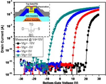
Fig. 1 Curves of drain current (Id) versus bottom-gate voltage (Vbg) for the dual-gate IGZO TFT at different top-gate voltages (Vtg).
In this letter, we propose a new AMOLED pixel circuit based on the concept of using the top gate of the dual-gate IGZO TFT to compensate the Vth difference. It consists of only three TFTs and two capacitors. The function of Vth compensation for this circuit is experimentally verified.
II. DEVICECHARACTERISTICS
Fig. 1 shows the curves of drain current (Id) versus bottom-gate voltage (Vbg) for the dual-bottom-gate IGZO TFT at different top-gate voltages (Vtg), with the schematic cross section and circuit symbol of the device in the inset. These transfer curves exhibit parallel shifts with respect to different Vtg values. This phenomenon is attributed to the attraction and expelling of free carriers in the active layer by the top gate. It implies that, using the bottom gate of the dual-gate a-IGZO TFT as the primary gate, Vth can be controlled by the top gate. This gives us a new idea of using it for the Vth compensation in the circuits. When the Vth of the Id–Vbg curve is positively shifted, a negative Vtg can move it back and vice versa. In other words, by appropriately setting the voltage on the top gate, the circuit of the TFT using the bottom gate can get rid of the problem of the Vth shift.
III. PROPOSEDCIRCUIT
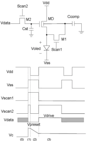
Fig. 2 shows the proposed AMOLED pixel circuit and its driving scheme. In the circuit, a dual-gate IGZO TFT is used as
394 IEEE ELECTRON DEVICE LETTERS, VOL. 33, NO. 3, MARCH 2012
Fig. 2 Proposed AMOLED pixel circuit and its driving scheme.
the driving TFT (MD), and two other conventional single-gate IGZO TFTs (M1 and M2) are used as switches. Two capacitors, namely, the storage capacitor Cst and the compensating capaci-tor Ccomp, are used to scapaci-tore the information of data voltage and Vth compensation, respectively. In addition, two control lines are needed to operate the pixel circuit.
Referring to Fig. 2, the operation of the pixel circuit is described in the following steps.
(0) Previous driving: For almost a frame time, M1 and M2 are off. The voltage stored in Cst sets the bottom gate of MD and thus determines the current and the illumination of the OLED.
(1) Precharge: M1 is turned on by Scan1 while Vdd and Vss are both at the high voltages so that Ccomp is charged to Vdd through MD and M1. Because of the same value of Vdd and Vss, there is no current through OLED during this period to minimize the unwanted illumination of the OLED.
(2) Compensation: Before the real data voltage (Vdrive) coming in, M2 is turned on by Scan2, and Vdata is kept at the preset voltage for compensation. Meanwhile, Vdd is converted to ground, and M1 keeps on. In such a case, Vc is discharged through M1 and MD and thus raises the Vth of MD. This discharge current stops when Vc comes to a voltage that changes the Vth of MD to match the preset voltage at the bottom gate to turn off the transistor. Therefore, the Vth of MD can be set at a predetermined value by the voltage at its top gate. During this period, OLED is in reverse bias to avoid the unwanted illumination of the OLED.
(3) Driving: After the compensation step, M1 is turned off by Scan1. Meanwhile, Vdd is converted to high voltage, and
Fig. 3 Measured waveforms of the proposed circuit.
Vss is toggled to ground. Vdrive is fed to the bottom gate of MD through M2 and stored in Cst to drive the OLED for a frame time.
IV. EXPERIMENTALRESULTS ANDDISCUSSION
Owing to the lack of device model for the simulation of the dual-gate TFT, the proposed AMOLED pixel circuit is veri-fied experimentally. The pixel circuit is composed of discrete components, where MD is a dual-gate IGZO TFT with 500-μm width and 10-μm length, M1 is a single-gate IGZO TFT with 500-μm width and 10-μm length, a single-gate a-Si TFT with 100-μm width and 10-μm length is used in place of OLED, and Ccomp is 10 pF. In the experiments, Vdata is fed directly to the bottom gate of MD instead of being driven through M2 and stored in Cst for simplification. Since the threshold voltage of IGZO TFT is usually smaller than 0 V, a diode-connected a-Si TFT substitutes for OLED to simulate the OLED func-tions. The off and on voltages for Vscan1 are −5 and 15 V. Furthermore, Vdata is modified to simulate the Vth variation from various devices. The positive and negative Vdata change is corresponding to negative and positive threshold voltage shift, respectively. For example, the preset voltage Vpreset of−6 V for compensation and driving voltage Vdrive of 12 V are synchronously increased or decreased 0.5 V to imitate that the Vth shifts negatively or positively for the same amount.
The experimental result for the proposed circuit is shown in Fig. 3. As can be seen, it is distinguishable in Vc that different sets of Vdata correspond to different discharge curves. For the lower Vdata input simulating the higher Vth, Vc is discharged to the higher value to compensate the Vth shift
TAI et al.: AMOLED PIXEL CIRCUIT WITH THRESHOLD VOLTAGE COMPENSATION FUNCTION 395
Fig. 4 Voled variation at different Vdata sets for the circuits with and without Vth compensation.
of MD. In such a case, the output voltage Voled converges to almost the same value. Namely, the compensation mecha-nism reduces the Vdata variation range of 2 V to only about 0.06-V difference in Voled, which verifies the circuits ability of Vth compensation. For a further issue, the top gate of MD can cause the threshold voltage shift during circuit operation. How-ever, in our compensation circuit, the top-gate voltage of the TFT is preset at a high voltage in advance and then discharged to a proper voltage in which the current flowing through the dual-gate TFT is extremely small. Therefore, although the top-gate field effect shifts with time, the compensation function can be still executed.
Fig. 4 compares the experimental results for the circuit with and without Vth compensation. The case without compensation is measured by disconnecting M1 and Ccomp to exclude the effect of the top-gate electrode, and the top gate of MD is grounded. The variation of Voled owing to the Vth shift of 2 V is up to about 0.4 V. According to the test results, the per-formance of compensation is obvious in the proposed circuit.
It is our intention to introduce the new concept of de-signing a circuit of dual-gate IGZO TFT with its bottom gate as the main gate electrode while using the top gate for Vth compensation. The application of the new concept is not limited to AMOLED circuits. It can be applied to other cir-cuits with the requirement of Vth compensation in the similar manner.
V. CONCLUSION
A voltage-driven AMOLED pixel circuit using the concept of the top gate of the dual-gate IGZO TFT to compensate the Vth variation is proposed. It uses only three n-type TFTs and two capacitors so that the aperture ratio of the display pixel can be large. The validity of the Vth compensation is experimentally verified.
ACKNOWLEDGMENT
The authors would like to thank AU Optronics Corporation for providing the dual-gate IGZO TFT device samples, through which the proposed circuit can be verified.
REFERENCES
[1] R. G. Stewart, “Active matrix OLED pixel design,” in Proc. SID Dig. Tech.
Papers, 2010, pp. 790–793.
[2] Y. J. Park, M. H. Jung, S. H. Park, and O. Kim, “Voltage-programming-based pixel circuit to compensate for threshold voltage and mobility using natural capacitance of organic light-emitting diode,” Jpn. J. Appl. Phys., vol. 49, no. 3, p. 03C D01, 2010.
[3] J. H. Lee, B. H. You, C. W. Han, K. S. Shin, and M. K. Han, “A new a-Si:H TFT pixel circuit suppressing OLED current error caused by the hysteresis and threshold voltage shift for active matrix organic light emitting diode,” in Proc. SID Dig. Tech. Papers, 2005, pp. 228–231.
[4] S. H. Jung, H. K. Lee, S. J. Park, T. J. Ahn, S. W. Lee, J. S. Yoo, S. Y. Yoon, C. D. Kim, and I. B. Kang, “A new AMOLED pixel com-pensating the combination of n-type TFT and normal OLED device,” in
Proc. SID Dig. Tech. Papers, 2009, pp. 1–4.
[5] S. H. Jung, H. S. Shin, J. H. Lee, and M. K. Han, “An AMOLED pixel for the VT compensation of TFT and a p-type LTPS shift register by employing 1 phase clock signal,” in SID Dig. Tech. Papers, 2005, pp. 300–303.
[6] H. S. Shin, J. H. Lee, J. H. Park, S. H. Choi, and M. K. Han, “Novel a-Si:H TFT Vth compensation pixel circuit for AMOLED,” in Proc.
ASID, 2006, pp. 466–469.
[7] M. K. Han, J. H. Lee, and W. J. Nam, “Thin film transistor (TFT) pixel design for AMOLED,” in Proc. IMID/IDMC Dig., 2006, pp. 413–418.
[8] D. Z. Peng, S. C. Chang, and Y. M. Tsai, “Novel pixel compensation circuit for AMOLED display,” in Proc. SID Dig. Tech. Papers, 2005, pp. 814–817.
[9] S. M. Choi, O. K. Kwon, N. Komiya, and H. K. Chung, “A self-compensated voltage programming pixel structure for active-matrix organic light emitting diodes,” in Proc. IDW Dig., 2003, vol. 10, pp. 535–538.
[10] G. R. Chaji and A. Nathan, “A stable voltage-programmed pixel circuit for a-Si:H AMOLED displays,” J. Display Technol., vol. 2, no. 4, pp. 347– 358, Dec. 2006.
[11] J. L. Sanford and F. R. Libsch, “TFT AMOLED pixel circuits and driving methods,” in Proc. SID Dig. Tech. Papers, 2003, pp. 10–13.
[12] S. J. Ashtiani, P. Servati, D. Striakhilev, and A. Nathan, “A 3-TFT current-programmed pixel circuit for AMOLEDs,” IEEE Trans. Electron Devices, vol. 52, no. 7, pp. 1514–1518, Jul. 2005.
[13] S. Ono, K. Miwa, Y. Maekawa, and T. Tsujimura, “VT compensation circuit for AM OLED displays composed of two TFTs and one ca-pacitor,” IEEE Trans. Electron Devices, vol. 54, no. 3, pp. 462–467, Mar. 2007.
[14] C. L. Lin and C. D. Tu, “Pixel circuit with high immunity to the degradation of TFTs and OLED for AMOLED displays,” in Proc.
IMID/IDMC/ASIA Display, 2008, pp. 473–476.
[15] B. W. Lee, I. H. Ji, S. M. Han, S. D. Sung, K. S. Shin, J. D. Lee, B. H. Kim, B. H. Berkeley, and S. S. Kim, “Novel simultaneous emission driving scheme for crosstalk-free 3D AMOLED TV,” in Proc. SID Dig.
Tech. Papers, 2010, pp. 758–761.
[16] K.-S. Son, J.-S. Jung, K.-H. Lee, T.-S. Kim, J.-S. Park, Y.-H. Choi, K. C. Park, J.-Y. Kwon, B. Koo, and S.-Y. Lee, “Characteristics of double-gate Ga–In–Zn–O thin-film transistor,” IEEE Electron Device
Lett., vol. 31, no. 3, pp. 219–221, Mar. 2010.
[17] K.-S. Son, J.-S. Jung, K.-H. Lee, T.-S. Kim, J.-S. Park, K. C. Park, J.-Y. Kwon, B. Koo, and S.-Y. Lee, “Highly stable double-gate Ga–In–Zn–O thin-film transistor,” IEEE Electron Device Lett., vol. 31, no. 8, pp. 812–814, Aug. 2010.
[18] N. D. Jankovic and V. Brajovic, “Vth compensated AMOLED pixel
employing dual-gate TFT driver,” Electron. Lett., vol. 47, no. 7, pp. 456– 457, Mar. 2011.