國 立 交 通 大 學
電信工程學系
博 士 論 文
使用標準矽製程整合 90°和 180°分合波器之
吉伯特微混頻器
Gilbert Micromixer with Integrated 90°/180°
Hybrids in Standard Si IC Process
研究生:曾聖哲
指導教授:孟慶宗
使用標準矽製程整合 90°和 180°分合波器之吉伯特
微混頻器
Gilbert Micromixer with Integrated 90°/180° Hybrids
in Standard Si IC Process
研究生:曾聖哲
Student:
Sheng-Che
Tseng
指導教授:孟慶宗 博士 Advisor:
Dr.
Chinchun
Meng
國立交通大學
電信工程學系
博士論文
A Dissertation
Submitted to Institute of Communication Engineering
College of Electrical Engineering
National Chiao Tung University
in Partial Fulfillment of the Requirements
for the Degree of Doctor of Philosophy
in
Communication Engineering
Hsinchu, Taiwan
使用標準矽製程整合 90°和 180°分合波器之吉伯
特微混頻器
學生:曾聖哲
指導教授:孟慶宗博士
Abstract (Chinese)
國立交通大學
電信工程學系博士班
摘
要
此論文中,以 0.35 毫米矽鍺雙載子互補式金氧半導體製程展示單端輸入輸 出吉伯特微混頻器。因應寬頻操作,在微混頻器中頻級使用電阻回授式轉阻放大 器,而在本地震盪級使用寬頻巴倫或是鼠徑耦合器來產生寬頻差動訊號。在研究 中,這些微波被動元件儘管實作在具損耗、低阻抗(~10 歐姆·公分)的矽基板上, 仍可產生很平衡的訊號。在第二章中,提出系統化的量測方式來評量混頻器每一 級的頻率響應。 第三章中提出可調式、電抗式正交相位產生器,其具有定值阻抗、低損耗、 雙頻帶實作和高正交相位精確度的特性。在所有頻率中,皆可達成正交相位輸出 與輸入匹配;而在設計的兩個頻段中,達成相同振幅輸出。實作的 2.4/5.2 GHz 正交相位降頻器之輸出振幅差小於 1 %、相位差小於 1;而實作的 2.4/5.7 GHz 單端頻譜升頻器具有高達 50 dB 單端頻譜抑制比。 第四章中,使用標準矽製程實作一個具有相位反轉器之寬頻鼠徑耦合器,並 詳細地分析損耗狀態下的耦合器。將相位反轉器應用在鼠徑耦合器,不僅能增加 頻寬,亦可提供等損耗的輸出路徑,以保持輸出平衡;而對稱式螺旋形共平面帶 狀傳輸線不僅可以縮小耦合器大小,還可利於建造相位反轉器於其中一個螺旋形 共平面帶狀傳輸線上。無失真具損耗的共平面帶狀傳輸線具有實數特性阻抗,使Abstract (Chinese) ii 得耦合器在中心頻率可達成匹配。此外,展示了應用此型態鼠徑耦合器之 2.5 到 13 GHz 寬頻微混頻器。 第五章中,實現整合本地震盪器級馬爾尚巴倫之寬頻混頻器,具有 15 dB 轉換增益,操作頻率在 3.5 到 14.5 GHz,此外,縮小化成塊元件馬爾尚之降頻 器展示於超寬頻系統中,具有 15.5 dB 轉換增益。而第六章中,以耦合指數和特 性阻抗來分析與設計傳統平面式馬爾尚巴倫與其變化型,此兩種型態在結構上具 有雙重性,然而當兩種巴倫以相同特性阻抗設計時,新型態巴倫會較寬頻。此外, 而在此章節分析中,發現只要實作在均質材料中,其輸出在所有的操作頻率皆會 具有相同的振幅與相反的相位,所以這兩種巴倫即使在具有損耗的環境中,仍可 正常運作。在實作結果中,改良式的馬爾尚巴倫明顯地具有較好的效能,其輸出 在 4 到 25 GHz 相位差約 180±5、振幅差約±0.5 dB,而其分數頻寬大於 140 %。 為了進一步比較,將此兩型態巴倫整合在微混頻器的本地訊號級,而相較於傳統 馬爾尚巴倫,改良型巴倫多提供 30 %操作頻寬。即使在具損耗的基板上,巴倫 消耗損耗大約只有 2~3 dB。 關鍵字:耦合指數、雙頻帶、馬爾尚巴倫、微混頻器、相位反轉器、正交、鼠徑 耦合器、矽鍺雙載子互補式金氧半導體、矽基板、寬頻。
Gilbert Micromixer with Integrated 90°/180°
Hybrids in Standard Si IC Process
Student: Sheng-Che Tseng
Advisor: Chinchun Meng
Department of Communication Engineering
National Chiao Tung University
Abstract
(English)
In this dissertation, all single-ended Gilbert micromixers are demonstrated using 0.35-m SiGe BiCMOS technology. For wideband operation, a transimpedance amplifier with resistive feedback is utilized in the IF stage while a broadband balun or a rat-race coupler is employed to generate wideband differential local oscillator (LO) signals. These microwave passive components in our study can generate truly balanced signals even in the presence of a lossy low-resistivity (~10 Ω·cm) silicon substrate. A systematic approach to measure the frequency response of each individual stage in a Gilbert mixer is developed in Chapter 2.
In Chapter 3, adjustable and reactive in-phase/quadrature (I/Q) generators with constant resistance are proposed with the properties of low loss, dual-band implementation, and high quadrature accuracy. The quadrature phase property and input matching of the I/Q generator can be achieved at all frequencies simultaneously. However, the magnitude balance of the dual-band I/Q generator is achieved at two designed frequencies. A 2.4/5.2 GHz I/Q down-converter and a 2.4/5.7 GHz single-sideband up-converter are demonstrated.
In Chapter 4, this dissertation realized a broadband uniplanar phase-inverter rat-race coupler using a standard silicon process, and then analyzed this coupler under
Abstract (English)
iv
a lossy condition. A phase inverter is employed in this coupler, not only to extend the operation bandwidth, but also to generate balanced outputs, while symmetrical spiral-shaped coplanar striplines (CPSs) are also utilized to shrink the coupler size, as well as to construct a phase inverter in the middle of one of spiral CPSs. The distortionless lossy CPS has a real characteristic impedance, and thus, perfect port matching of the coupler can be achieved. A wideband Gilbert micromixer with an LO rat-race coupler is demonstrated and works from 2.5 to 13 GHz.
In Chapter 5, the wideband mixer with an integrated LO Marchand balun has the conversion gain of 15 dB and works from 3.5 to 14.5 GHz. In addition, a 15.5-dB conversion gain Gilbert mixer with a miniaturized lumped-element Marchand balun is demonstrated for UWB applications. In Chapter 6, a planar Marchand balun and its modification are analyzed and designed with a coupling factor and a corresponding characteristic impedance. The modification has duality with the original Marchand balun in structure. However, this proposed alteration has a much larger operation bandwidth than the prototype. Additionally, based on our analysis, the fact is found that the balun’s outputs are always equal in magnitude and opposite in phase within all frequency ranges, as long as the material is homogeneous. Namely, these baluns, even in a lossy material, still function well. The implemented modified Marchand balun has a better performance with outputs of an 180±5 phase difference and a ±0.5-dB magnitude imbalance from 4 to 25 GHz. The fractional bandwidth is more than 140%. Also, the modified Marchand balun integrated at the LO stage of the mixer offers more than 30%-operation bandwidth.
Keywords: Coupling factor, dual-band, Marchand balun, micromixer, phase inverter, quadrature, rat-race coupler, SiGe BiCMOS, silicon substrate, wideband.
Acknowledgements
一路走來感謝的人太多,首先感謝指導老師孟慶宗教授,碩博五
年來指導與教誨,不辭辛苦,給予學生許多學習與發展的機會,使學
生得以完成學業、在學術上有所貢獻;感謝評審老師,吳重雨校長、
呂學士教授、呂良鴻教授、洪子聖教授、莊惠如教授、張志揚教授、
鍾世忠教授、郭仁財教授,遠道而來參與學生的博士論文口試,提供
指導與建議;交通大學提供了很好的學習與研究環境,系上師長們奠
定了學生的專業基礎,而學校提供完善的設備,得以讓學生發揮所
長;還要感謝國家晶片系統設計中心提供晶片實作機會,國家奈米元
件實驗室高頻技術中心黃國威博士以及其團隊提供量測協助。感謝聯
發科技基金會的賞識,提供學生優渥的獎學金。
對於一同研究的學長姐、同學、學弟妹們,也感激萬分,學長吳
宗翰、林明奇、陳為昱、陳慶鴻、鍾智琦、李紹宇、李仰涵,學姊蘇
珍儀,同學張宇文、吳智凱、吳澤宏,學弟魏宏儒、張家宏、廖樺輿、
顏英杰、李約廷、吳柏誼、游勝文、欉冠璋、陳威宇、徐金詳、陳揚
鮮、陸熙良、羅泰麟、王大維、林士峰、林忠佑、張智凱,學妹李宜
珊、林宜蓁、鄧雅惠、簡欣怡、王嘉苓,由於你們,研究才能如此順
利;由於你們,生活才不會苦悶;感激的話非三言兩語可以說盡,這
Acknowledgements vi
五年來的歡笑與淚水,將成為我人生最美好回憶。
感謝爸爸、媽媽、阿姨、姊姊、大哥與二哥的支持,讓我在求學
的路途平順、衣食無憂;要感謝的人太多了,今日的成果,因為有大
家,才如此豐碩,願此榮耀與大家共享。
NCTU, July 2008Table of Contents
ABSTRACT (CHINESE)...I ABSTRACT (ENGLISH) ...III ACKNOWLEDGEMENTS ...V TABLE OF CONTENTS ... VII LIST OF FIGURES...XI LIST OF TABLES ... XVII LIST OF ABBREVIATIONS AND SYMBOLS...XIX
CHAPTER 1 INTRODUCTION...1
1.1 MILLIMETER-WAVE ANDMICROWAVE INSILICON...1
1.2 SILICON-BASEDPASSIVECOMPONENTS...5
1.3 RESEARCHWORKS...9
CHAPTER 2 WIDEBAND MICROMIXER ...11
2.1 INTRODUCTION...11
2.2 CIRCUITDESIGN...12
2.3 MEASUREMENTRESULTS...15
2.4 SUMMARY...19
CHAPTER 3 ADJUSTABLE AND REACTIVE I/Q GENERATOR WITH CONSTANT RESISTANCE FOR DOWN- AND UP-CONVERTERS ...21
3.1 INTRODUCTION...21
3.2 REACTIVEI/Q GENERATOR...23
3.2.1 Wideband Reactive I/Q Generator With Constant Resistance ...24
3.2.2 Dual-Band and Adjustable I/Q Generator With Constant Resistance...26
3.3 CIRCUITDESIGN...30
3.4 MEASUREMENTRESULTS...33
3.4.1 2.4 GHz and 5.2 GHz I/Q Down-Converter...33
3.4.2 2.4 GHz and 5.7 GHz SSB Up-Converter ...36
3.5 SUMMARY...40
CHAPTER 4 SILICON MONOLITHIC PHASE-INVERTER RAT-RACE COUPLER USING SPIRAL CPSS ...41
4.1 INTRODUCTION...41
4.2 ANALYSIS ANDDESIGN OFRAT-RACECOUPLERSWITH APHASEINVERTER.43 4.3 MEASUREMENTRESULTS...50
Table of Contents
viii
4.3.1 Micromixer With an Integrated Phase-Inverter Rat-Race Coupler ...50
4.3.2 Symmetrical Spiral-Shaped Phase-Inverter Rat-Race Coupler ...55
4.3.3 Distortionless Transmission Line ...60
4.4 SUMMARY...62
CHAPTER 5 MONOLITHIC PLANAR MARCHAND BALUN USING A STANDARD SILICON IC PROCESS.65 5.1 INTRODUCTION...65
5.2 ANALYSIS ANDIMPLEMENTATION OF THEPLANARMARCHANDBALUNUSING ASILICONIC PROCESS...66
5.2.1 Analysis...66
5.2.2 Implementation ...70
5.2.3 Lumped-Element Marchand Balun ...72
5.3 MEASUREMENTRESULTS...73
5.3.1 Planar Marchand Balun ...73
5.3.2 Micromixer With an Integrated Marchand Balun...76
5.3.3 Micromixer With a Miniaturized Marchand Balun for UWB Applications ...82
5.4 SUMMARY...88
CHAPTER 6 STANDARD SILICON-BASED WIDEBAND BALUN DESIGN WITH COUPLING FACTOR AND CHARACTERISTIC IMPEDANCE ...91
6.1 INTRODUCTION...91
6.2 ANALYSIS AND DESIGN OF BROADBAND BALUNS ON ASTANDARD SILICON SUBSTRATE...93
6.2.1 Analysis in the Case of Loss ...94
6.2.2 Analysis in Bandwidth ...97
6.2.3 Implementation ...102
6.3 MEASUREMENTRESULTS...103
6.3.1 Basic Marchand Balun With Edge Coupling and Its Modification With Broadside Coupling...103
6.3.2 Micromixers With an Integrated LO Wideband Balun ...107
6.4 SUMMARY... 111
CHAPTER 7 CONCLUSION...113
REFERENCES ... 117
APPENDIX A DERIVATION OF S21=-S41IN THE PHASE-INVERTER RAT-RACE COUPLER ...125
APPENDIX B DERIVATION OF THE NORMALIZED CHARACTERISTIC IMPEDANCE AND S21OF THE CPSS FOR THE PERFECT PORT-MATCHING ... 127
Table of Contents
APPENDIX D DERIVATION OF THE EVEN-MODE TRANSMISSION COEFFICIENT OF THE BALUNS...133
APPENDIX E INPUT MATCHING CRITERIA FOR THE BASIC AND MODIFIED MARCHAND BALUNS IN THE LOSSLESS CASE ...135
APPENDIX F MATHEMATICS ... 137
APPENDIX G PROPERTIES OF MATERIAL AND METALS ...139
ABOUT THE AUTHOR...141
List of Figures
Chapter 1
Fig. 1-1 Average atmospheric absorption rate of millimeter-waves...2
Fig. 1-2 Applications at millimeter-wave and microwave frequencies...2
Fig. 1-3 Millimeter-wave and microwave solutions...3
Fig. 1-4 Evolution of chip size, device performance, and operation frequency in silicon...3
Fig. 1-5 77-GHz phase-array antenna system. ...3
Fig. 1-6 Silicon technology development in TSMC...4
Fig. 1-7 Throughput of each TSMC CMOS technology. ...4
Fig. 1-8 R&D cost for silicon processes...5
Fig. 1-9 Silicon-based system-on-chips...5
Fig. 1-10 New design concepts for high-frequency applications. ...6
Fig. 1-11 Quarter-wavelength and transmission coefficient with respect to operation frequencies with assumption of εeff= 8. ...9
Chapter 2 Fig. 2-1 Schematic of the micromixer with a TIA output buffer. ...12
Fig. 2-2 Cherry Hooper technique employed in the micromixer...13
Fig. 2-3 Small signal models of (a) the transconductance amplifier and (b) the transimpedance amplifier. ...14
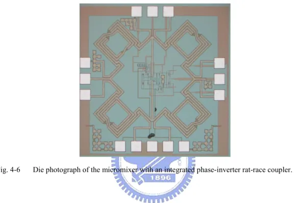
Fig. 2-4 Die photograph of the micromixer...15
Fig. 2-5 Conversion gain of the micromixer with respect to RF frequencies. ....16
Fig. 2-6 Conversion gain of the micromixer with respect to IF frequencies...17
Fig. 2-7 Conversion gain of the micromixer with respect to LO power...18
Chapter 3 Fig. 3-1 Quadrature generators with the C-R and R-C sections or with the C-R and L-R sections...24
Fig. 3-2 Magnitude ratio ( | VA /VB | ) and phase error of the reactive I/Q generator with respect to normalized frequency ω0...26
Fig. 3-3 Topology of the dual-band I/Q generator...27
Fig. 3-4 Magnitude ratio ( | VA_dual/VB_dual | ) and phase error of the dual-band reactive I/Q generator with respect to normalized frequency ω0= ωl. .29 Fig. 3-5 Schematic of the dual-band I/Q down-converter. ...31
Fig. 3-6 Schematic of the dual-band SSB up-converter. ...31
List of Figures
xii
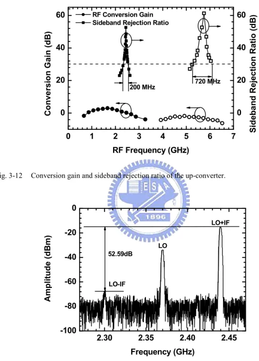
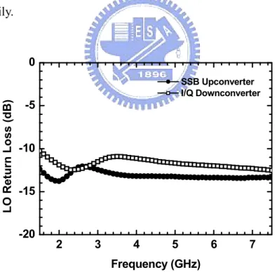
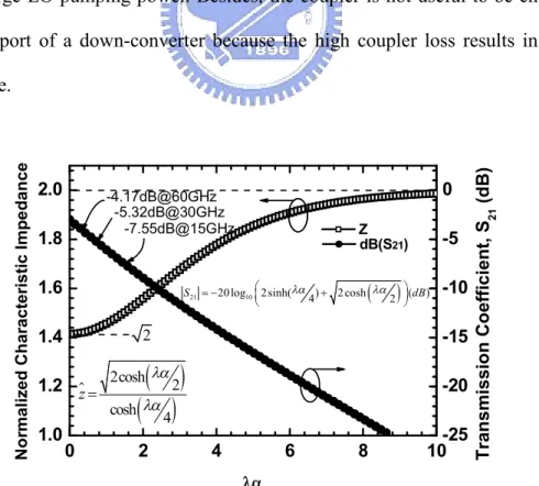
Fig. 3-8 Die photographs of (a) the 2.4/5.2-GHz I/Q down-conversion mixer and (b) the 2.4/5.7-GHz SSB up-conversion mixer...33 Fig. 3-9 Conversion gain of I and Q channels of the dual-band I/Q down-conversion mixer...34 Fig. 3-10 Output phase and amplitude balance for the dual-band I/Q downconverter...35 Fig. 3-11 Port-to-port isolations of the dual-band I/Q downconverter. ...36 Fig. 3-12 Conversion gain and sideband rejection ratio of the up-converter. ...37 Fig. 3-13 Output spectrum of the dual-band SSB up-converter at 2.4 GHz. The side-band rejection ratio is 52.59 dB. ...37 Fig. 3-14 Output spectrum of the dual-band SSB up-converter at 5.7 GHz. The side-band rejection ratio is 62.85 dB. ...38 Fig. 3-15 Port-to-port isolations of the dual-band SSB up-converter...38 Fig. 3-16 LO return loss of the dual-band I/Q down-converter and SSB up-converter. ...39
Chapter 4
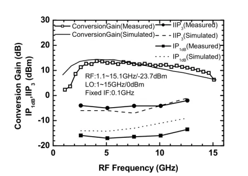
Fig. 4-1 Rat-race coupler evolution...42 Fig. 4-2 Even- and odd-mode analyses of a phase-inverter rat-race coupler. ...44 Fig. 4-3 Normalized characteristic impedance and transmission coefficient with respect to λα for perfect matching. ...47 Fig. 4-4 Symmetrical spiral-shaped CPS rat-race coupler with a phase inverter.49 Fig. 4-5 Schematic of the micromixer with a phase-inverter rat-race coupler. ...50 Fig. 4-6 Die photograph of the micromixer with an integrated phase-inverter rat-race coupler...51 Fig. 4-7 Conversion gain, IP1dB, and IIP3 of the phase-inverter rat-race coupler
micromixer. ...52 Fig. 4-8 Noise figure of the micromixer with an integrated phase-inverter rat-race coupler...53 Fig. 4-9 Conversion gain of the micromixer with an integrated phase-inverter rat-race coupler with respect to IF frequencies...53 Fig. 4-10 Port-to-port isolations of the micromixer with an integrated phase-inverter rat-race coupler...54 Fig. 4-11 Return loss of the micromixer with an integrated phase inverter rat-race coupler...54 Fig. 4-12 Die photograph of the symmetrical spiral-shaped rat-race coupler with a phase inverter. ...56 Fig. 4-13 S-parameters of the symmetrical spiral-shaped rat-race coupler with a
List of Figures
phase inverter. ...57
Fig. 4-14 Phase difference between S21and S41of the rat-race coupler with a phase inverter. ...57
Fig. 4-15 Phase difference between S23and S43of the rat-race coupler with a phase inverter. ...58
Fig. 4-16 Dissipated loss of the symmetrical spiral-shaped rat-race coupler with a phase inverter. ...58
Fig. 4-17 Input return loss of the symmetrical spiral-shaped rat-race coupler with a phase inverter. ...59
Fig. 4-18 Calculated S-parameters of the rat-race coupler with a phase inverter..61
Fig. 4-19 Calculated characteristic impedance and complex propagation constant of the rat-race with a phase inverter...62
Chapter 5 Fig. 5-1 Planar Marchand balun with λ/4 coupled lines...66
Fig. 5-2 S-parameter derivation of the planar Marchand balun with λ/4 coupled lines. ...68
Fig. 5-3 S-parameter derivation of the planar Marchand balun. ...69
Fig. 5-4 Magnitude of the transmission and reflection at the input port of the planar Marchand balun with respect to coupling factor k for the cases of no loss. ...70
Fig. 5-5 Schematic of the lumped-element Marchand balun...72
Fig. 5-6 Die photograph of a monolithic Marchand balun.. ...73
Fig. 5-7 Input return loss of the planar Marchand balun. ...74
Fig. 5-8 Transmission coefficients of the planar Marchand balun. ...75
Fig. 5-9 Phase and magnitude errors of the planar Marchand balun...75
Fig. 5-10 Dissipated loss of the Marchand balun. ...76
Fig. 5-11 (a) Schematic and (b) die photograph of the micromixer with an LO Marchand balun and a TIA output buffer...77
Fig. 5-12 Return loss of the micromixer with an integrated planar Marchand balun. ...78
Fig. 5-13 Conversion gain of the micromixer with an integrated planar Marchand balun...79
Fig. 5-14 Port-to-port isolations of the micromixer with an integrated planar Marchand balun. ...80
Fig. 5-15 IP1dB and IIP3 of the micromixer with an integrated planar Marchand balun...81 Fig. 5-16 Noise figure of the micromixer with an integrated planar Marchand
List of Figures
xiv
balun...81 Fig. 5-17 Die photograph of the lumped-element Marchand balun ...82 Fig. 5-18 Scattering parameters of the lumped-element Marchand balun. ...83 Fig. 5-19 Output phase difference and dissipated loss of the lumped-element Marchand balun. ...83 Fig. 5-20 Schematic of the UWB Gilbert down-conversion mixer with an LO lumped-element Marchand balun. ...84 Fig. 5-21 Die photograph of the lumped-element Marchand balun micromixer...84 Fig. 5-22 Conversion gain, IP1dB and IIP3 of the UWB Gilbert down-conversion
mixer with an LO lumped-element Marchand balun with respect to RF frequencies. ...85 Fig. 5-23 Conversion gain and noise figure of the UWB Gilbert down-conversion mixer with an LO lumped-element Marchand balun with respect to IF frequencies. ...86 Fig. 5-24 Port-to-port isolations of the UWB Gilbert down-conversion mixer with an LO lumped-element Marchand balun. ...87 Fig. 5-25 Return loss of the UWB Gilbert down-conversion mixer with an LO lumped-element Marchand balun. ...87
Chapter 6
Fig. 6-1 Wideband baluns based on two λ/4 coupled lines. ...92 Fig. 6-2 Even- and odd-mode analyses of the basic and modified Marchand baluns. ...94 Fig. 6-3 Operation bandwidth analysis of the lossless modified Marchand balun. ...99 Fig. 6-4 Operation bandwidth analysis of the lossless basic Marchand balun. .100 Fig. 6-5 S11and S21 of the lossy modified balun with respect to the coupled-line
quality factor. ...101 Fig. 6-6 Maximum S21 of the lossy baluns with respect to the quality factor and
coupling factor. ...102 Fig. 6-7 3D views of the basic and modified Marchand baluns. ...103 Fig. 6-8 Die photographs of the basic Marchand balun and its modification. ..104 Fig. 6-9 S-parameters of the basic Marchand balun. ...105
Fig. 6-10 S-parameters of the modified Marchand balun...106
Fig. 6-11 Output imbalance of the basic and modified Marchand baluns...106 Fig. 6-12 Schematic of the micromixer with an integrated LO wideband balun.107 Fig. 6-13 Die photographs of the micromixers with a basic Marchand balun and with a modified Marchand balun. ...108
List of Figures
Fig. 6-14 Conversion gain, IP1dB, and IIP3 of the micromixers with a basic
Marchand balun and with a modified Marchand balun. ...109 Fig. 6-15 Noise figure and conversion gain of the micromixers with a basic Marchand balun and with a modified Marchand balun. ...109 Fig. 6-16 Port-to-port isolations of the micromixers with a basic Marchand balun and with a modified Marchand balun. ...110 Fig. 6-17 Return loss of the micromixers with a basic Marchand balun and with a modified Marchand balun...110
Chapter 7
Fig. 7-1 From Inductors to Lossy Transmission Lines...114 Fig. 7-2 Millimeter-wave and microwave silicon-based transceiver...116 Appendix C
Fig. C-1 Four-port network of the coupled line. ...129 Fig. C-2 Electric circuit model of a transmission line for the even mode...129
List of Tables
TABLE 2.1 Measurement Results of the Wideband Micromixer ...18 TABLE 3.1 Calculated Inductance and Capacitance for Dual-Band Wi-Fi I/Q Generators. ...29 TABLE 3.2 Adjustable Mechanism for Four I/Q Mismatch Conditions. ...32 TABLE 3.3 Measurement Results of the Tunable Dual-Band I/Q Down-Converter and SSB Up-Converter ...40 TABLE 4.1 Measurement Results of the Phase-Inverter Rat-Race Coupler Mixer..55 TABLE 4.2 Comparisons of the Silicon-Based Rat-Race Couplers With a Phase Inverter. ...60 TABLE 5.1 Measurement Results of the Implemented Marchand Baluns and Their Applications in Mixers...88 TABLE 6.1 Comparison between Basic Marchand Balun and Modified Marchand Balun ... 111 TABLE 6.2 Comparison in Theory between Basic Marchand Balun and Modified Marchand Balun... 111 TABLE 7.1 Comparison between Marchand Baluns and Phase-Inverter Rat-Race Couplers ...115
List of Abbreviations and Symbols
Abbreviations
BiCMOS Bipolar Complementary Metal Oxide Semiconductor CG Conversion Gain
CPS Coplanar Stripline CPW Coplanar Waveguides EM Electromagnetic
FGCPW Finite-Ground Coplanar Waveguide GSGSG Ground–Signal–Ground–Signal–Ground HBT Hetero-junction Bipolar Transistor
I/OP1dB Input/Output 1-dB Gain Compression Point
I/OIP3 Input/Output Third-Order Intercept Point
I/Q In-Phase/Quadrature IC Integrated Circuit LO Local Oscillator
NF Noise Figure
pMOS p-channel MOSFET RFICs RF Integrated Circuits SiGe Silicon-Germanium SSB Single Side-Band
TCA Transconductance Amplifier TIA Transimpedance Amplifier UWB Ultra-Wideband
WiMAX Worldwide Interoperability for Microwave Access WLAN Wireless Local Area Network
Symbols
α Attenuation constant
β Propagation constant
γ Complex propagation constant
λ Wavelength
ω0 Operating frequency, resonant frequency ωtransition Transition frequency
List of Abbreviations and Symbols
xx
fT Cut-off frequency
gm Transconductance of a transistor
k Coupling factor
z Normalized characteristic impedance with respect to Z0
z Complex normalized characteristic impedance with respect to Z0
Q Quality factor
R0, L0, G0, C0 Per-unit-length resistance, inductance, conductance, and capacitance R, I, C, T Reflection, isolation, coupling, and through coefficients of the coupled
line
Y0e Even-mode characteristic admittance Y0o Odd-mode characteristic admittance Z0 Terminal impedance
Z0e Even-mode characteristic impedance Z0o Odd-mode characteristic impedance ZC Characteristic impedance
Chapter 1 Introduction
1.1 M
ILLIMETER-W
AVE ANDM
ICROWAVE INS
ILICONHigh data rate and wide bandwidth wireless communication systems are easily feasible in millimeter-wave and microwave frequencies. Recently, many applications are booming in millimeter-wave and microwave bands thanks to the advance of the semiconductor technologies and wireless communication techniques, such as the high-speed wireless local area network, automotive collision avoidance radar, image sensing, and so on. The demand of the wireless communication services stimulates the researches of the millimeter-wave and microwave circuit design.
The more than 30-GHz millimeter-wave band has a broad bandwidth and low interference, because of the high absorption rate in the air, as shown in Fig. 1-1. In the past, the applications in this band were not popular due to the device characteristics and integration techniques. However, up to now, many studies and techniques have been developed for the millimeter-wave and microwave applications, for instance, device and package technologies. In Europe, America, and Japan, the frequency resource is also planed. Now, applicable bands include 24 GHz for microwave Doppler sensors, 38 GHz for short-haul transmission-links, 57-66 GHz for WiHD, 76-77 GHz for automotive radars, 77-81 GHz for automotive short-haul radars, 71-76, 81-86, 92-95 GHz for wireless wideband communications, as shown in Fig. 1-2. The applications cover livelihood, satellite communication, astronomy, and national defense. The profits from the millimeter-wave and microwave applications are more than one hundred million dollars in the whole world. Therefore, the millimeter-wave and microwave researches should be at the high priority.
Introduction
2
Fig. 1-1 Average atmospheric absorption rate of millimeter-waves.
24 Microwave Doppler Sensors
38 Short-Haul Transmission-Links 57 WiHD 76 Automotive Radars 77 Automotive Short-Haul Radars
71 81 92
Wireless Wideband Communications
GHz
66 86 95
Fig. 1-2 Applications at millimeter-wave and microwave frequencies.
Three solutions are shown in Fig. 1-3 for the millimeter-wave and microwave applications. In the past, the front-end was fabricated only using GaAs processes due to device performances. However, the reliability and productivity of GaAs technology are low. Moreover, the GaAs front-end cannot be integrated into the CMOS baseband IC. Fig. 1-4 describes the silicon evolution and reveals that chip size is getting bigger while device operation frequency is getting high. Advanced deep sub-micron silicon-based technologies have made the silicon devices with > 100-GHz cut-off frequency possible and thus the era of silicon millimeter wave is impending. Millimeter-wave system-on-chip (SOC) will become a reality because of the high integration and low-cost production of the silicon fabrication processes. Even,
1.1 Millimeter-Wave and Microwave in Silicon
77-GHz antennas are also integrated on chips in Fig. 1-5.
CMOS Front-End IC CMOS Baseband IC GaAs PA CMOS Baseband IC GaAs Front-End IC & PA GaAs-Based Solution Silicon-Based SOC Solution
Fig. 1-3 Millimeter-wave and microwave solutions.
Fig. 1-4 Evolution of chip size, device performance, and operation frequency in silicon.
Fig. 1-5 77-GHz phase-array antenna system [Hajimiri, ISSCC 2006].
T=1/fT die size 2000 1990 1980 2010 Time T=1/fT die size 1mm 10mm 100mm 6 6..88mmmm 7 777GGHHzzOOnn--CChhiipp A Anntteennnnaaxx44 3 3..88mmmm
Introduction
4
According to the TSMC technology development in Fig. 1-6, the 32-nm process is developing now and the 45-nm is at the production level for logic circuits, whereas the RF circuits can be fabricated using advanced technologies like a 65-nm CMOS process. Fig. 1-7 describes the throughput of each TSMC CMOS technology. The R&D cost is the most important issue when the mask cost increases tremendously for the advanced technologies, as shown in Fig. 1-8. Nevertheless, the advance in silicon processes is not good for scale-down of the front-end chips since passive components in front-end circuits dominate chip size. As shown in Fig. 1-9, the area of the RF front-end does not shrink obviously with the technology advance and the ratio of the front-end part is getting higher. Therefore, the passives affect not only the front-end performances but also the entire cost, and the research topic in this dissertation is the size and performance of the passive components.
Fig. 1-6 Silicon technology development in TSMC.
1.2 Silicon-Based Passive Components
Fig. 1-8 R&D cost for silicon processes [Morris Chang, “Foundry Future: Challenges in the 21st Century”, in ISSCC 2007].
(a) (b) (c)
Fig. 1-9 Silicon-based system-on-chips (a)Atheros[JSSC2004] 0.25um (RF:23mm2)
(b)Atheros[ISSCC 2006] 0.18um (RF:13.5mm2) (c)DICE[JSSC2006] 90nm (RF:12mm2).
1.2 S
ILICON-B
ASEDP
ASSIVEC
OMPONENTSThe era of the wireless applications with high data-rate transmission and multiple functions is coming, e.g., the IEEE 802.11a/b/g combo system [1], ultra-wideband (UWB) system [2], and WiMAX system [3]. The range of carrier frequencies and their bandwidth constantly increase. The obligation of the complicated data processing belongs to the baseband design, while the RF integrated circuit (IC) design takes responsibility for the wide range frequency and broad bandwidth operation. Nevertheless, the design of the high-frequency and wideband RF circuits is a big challenge in the overall solution implementation. For an active mixer, the transistors have natural instinct to perform wide range and broad bandwidth frequency translation. Due to the input/output matching networks, narrowband passive
Tech. Cost (Wafer/Maskset)
0.18m 1.4K/120K
0.13m 1.8K/300K
90 nm 2.5K/900K
Introduction
6
components, and loading effects, the mixer’s wideband ability is restricted. Hence, microwave broadband passive components, such as Marchand baluns and rat-race couplers, can be integrated into ICs for wideband applications.
The silicon radio-frequency/microwave integrated circuit revolution has brought inductors and transformers into integrated circuits. As the silicon circuit reaches the millimeter-wave regime, new circuit design concepts arise. In our researches, a
CR-LR quadrature generator takes the place of a polyphase filter while inductors and
transformers along with parasitic capacitance operate as a transmission line and a coupled line, respectively, as shown in Fig. 1-10. The inductor absorbing parasitic capacitors to form a transmission line enables the high frequency operation. It is now feasible to integrate passive components based on quarter-wavelength transmission lines in the integrated circuits.
C
L
C
R
R
C
R
R
0
90
90
0
L R C INV
VA B V
Fig. 1-10 New design concepts for high-frequency applications.
Silicon-based technologies have the properties of high integration and low-cost production. Active devices have advanced in possession of the cut-off frequency of more than 100 GHz, and they are suitable for microwave and millimeter-wave applications [4]. Today, passive components are largely implemented using silicon-based technologies in the RFICs. For example, inductors and transformers are
1.2 Silicon-Based Passive Components
applied in oscillators, low-noise amplifiers, and mixers [5]. However, the standard silicon substrate with a resistivity of approximately 10 ·cm deteriorates signals, causes crosstalk between two adjacent passives, and influences the functions of passive components. Thus, it is a big challenge to form useful RF passive components on a silicon substrate for microwave and millimeter-wave applications [6], [7].
To reduce the substrate loss, many solutions have been developed, such as micromachining, high-resistivity substrate, silicon-on-insulator (SOI) process and shielding. Abidi et al. applied the front-side micromachining to form a suspended inductor in a CMOS RF amplifier. Thus, this inductor has higher self-resonance frequency and quality factors and can work at higher frequencies [8]. The backside micromachining is also employed to eliminate the unpredictable pattern-dependent etching behavior of front-side micromachining [9], [10]. Besides this, the high-resistivity (~1 k·cm) silicon substrate is also employed, but the entire substrate with high resistivity is not compatible with active devices, due to the latch-up issue [11]. The local high-resistivity substrate can be obtained by proton-damaged ion implantation with high energy (15 MeV) before the backend process, or with low energy (~4 MeV) after the backend process [12]. The substrate resistivity increases significantly to ~1 M·cm. The performances of the transmission lines and spiral inductors on the proton-damaged high-resistivity silicon substrate are enhanced [12], [13]. Shielding, like patterned ground shields [14] and floating shields [7], is inserted between the signal path and the silicon substrate, to resist the substrate loss without any extra process. This method is adequate for the process with multiple metal layers.
In this dissertation, our passive components function well in standard silicon-based IC processes because of the new design concepts such as balanced path loss and distortionless transmission lines. The implementation directly on the silicon
Introduction
8
substrate is good for size compactness thanks to the high dielectric constant. Meander lines compress the size while stepped-impedance and lumped-element techniques shrink the transmission-line length further as well as reducing the loss. In this dissertation, it shows that passive components such as CR-LR reactive quadrature generators, ring hybrids, and Marchand baluns could be successfully integrated into standard silicon-based ICs.
As shown in Fig. 1-10, the proposed reactive quadrature generator is derived from the conventional C-R and R-C sections. The low-pass session, R-C section, is substituted by the L-R network. The truly balanced quadrature signals are generated when R=ω0L=(ω0C)-1. Regardless of frequencies, the input impedance equals R and
the output signals are always in quadrature. When compared with a polyphase filter, this reactive quadrature generator has three advantages. 1) The generator has low loss thanks to the absence of resistors and is suitable for high-frequency applications. 2) The input impedance is constant and the wideband matching is achievable. 3) A multi-band quadrature generator can be established by increasing the order of the L-C networks.
A wideband phase-inverter rat-race coupler and a broadband Marchand balun are presented to demonstrate the new design concept of the transmission lines and coupled lines for silicon-based millimeter-wave ICs, respectively. Our microwave passives are directly implemented on a lossy silicon substrate. The transmission-line length of passive components reduces with operation frequency increase and so does the loss, as shown in Fig. 1-11. Therefore, the rat-race coupler and Marchand balun operate better at millimeter-wave frequencies. The passive components and the proposed design approaches can be applied for the millimeter-wave regime.
1.3 Research Works 0 20 40 60 80 100 -20 -10 0 102 103 S21(Marchand Balun)=1cm-1 S21(Marchand Balun)=2cm-1 S21(Marchand Balun)=3cm-1 S21(Rat-Race Coupler)=1cm-1 S21(Rat-Race Coupler)=2cm-1 S21(Rat-Race Coupler)=3cm-1 T ra n s m is s io n C o e ff ic ie n t, S 21 (d B ) Frequency (GHz) Quarter Wavelength Q u a rt e r W a v e le n g th , /4 ( m )
Fig. 1-11 Quarter-wavelength and transmission coefficient with respect to operation frequencies with assumption of εeff= 8.
1.3 R
ESEARCHW
ORKSChapter 2 depicts a wideband micromixer and monitors the frequency response of each stage of the mixer. Chapter 3 offers a novel adjustable and reactive quadrature generator for wideband or dual-band applications. Chapter 4 analyzes and designs a phase-inverter rat-race coupler with spiral-shaped coplanar striplines (CPSs) in the present of loss. The Marchand balun design concept and the measured results of a monolithic planar Marchand balun are represented in Chapter 5. The optimal design of the lossy Marchand balun and its modification are proposed in Chapter 6. The implemented circuits are described as follows:
Wideband Gilbert micromixer
Dual-band I/Q down-converter with an adjustable and reactive LO quadrature generator
Dual-band SSB up-converter with an adjustable and reactive LO quadrature generator
Introduction
10
Phase-inverter rat-race coupler with spiral-shaped CPSs
Wideband Gilbert micromixer with a phase-inverter rat-race coupler Planar Marchand balun
Lumped-element Marchand balun Modified Marchand balun
Wideband Gilbert micromixer with an integrated LO Marchand balun Wideband Gilbert micromixer with a lumped-element Marchand balun
Chapter 2 Wideband Micromixer
2.1 I
NTRODUCTIONFor the wideband circuit design, the wideband matching of the input/output ports is a significant issue. The common implemented active mixer is a Gilbert mixer using the emitter-coupled differential input stage. Owing to the high input impedance of the common-emitter-configured transistors, the reactive or resistive matching is needed at the input port. For the reactive matching, the matching bandwidth relates to the orders of the passive matching network. Increasing the order of the matching network can expand the operation bandwidth, but also takes more area. Although the resistive matching can perform wideband matching, it also introduces loss. The variant of the Gilbert mixer, the so-called micromixer, which is defined as a microwave mixer in [15], has the properties of the wideband input matching and single-ended input. Those properties facilitate the realization of the wideband and single-ended mixer. In this work, the input stage of the mixer is made up of the micromixer.
High impedance resistors or active pMOS loads are usually employed to obtain high conversion gain. In addition, the pMOS current mirror is used to effectively combine the differential IF output current signals of the mixer and establish a single-ended output. However, the high impedance causes a low-frequency pole at the output stage, which slows down the IF response. The transimpedance amplifier (TIA) with resistive feedback is, hence, utilized at the output stage to reduce the output impedance and extend the bandwidth in this work [16], [17]. A single-ended wideband Gilbert down-converter is fabricated in the 0.35-m SiGe BiCMOS technology and demonstrated in this chapter. A technique to measure the RF, LO, and IF stages of a Gilbert mixer is developed as well.
Wideband Micromixer
12
2.2 C
IRCUITD
ESIGNThe entire schematic of the single-ended wideband down-converter is shown in Fig. 2-1. This down-converter is formed by the micromixer and the TIA output buffer. Each element has the broadband property. The micromixer can be considered as the combination of two single-balanced mixers. One mixer is formed by the common emitter-configured RF amplifier Q2; the other is composed of the
common-base-configured RF amplifier Q3. The LO switch quad is made up of the transistors Q5, Q6, Q7, and Q8. The current mirror pair Q1 and Q2provides the balance dc currents in the
RF input stage and then these two RF amplifiers have equal magnitude and opposite phase transconductance gain to obtain good mixer balance. Moreover, the diode-type transistor Q1 reduces the input impedance of Q2 and enhances the speed of the
common-emitter-configured input stage. The input impedance is controlled by the transistors Q1 and Q3 and the resistors r1 and r3. It is easy to achieve wideband
matching so this micromixer can act as a wideband mixer [18].
2 CC V 1 CC V
RF
IF
1 Q Q2 3 Q Q4 1 r r2 3 r r4TIA Output Buffer
LO+
LO-5 Q Q6 Q7Q8 9 Q 10 Q 1 M M2 r5 r6 Gilbert Micromixer Fig. 2-1 Schematic of the micromixer with a TIA output buffer.2.2 Circuit Design
To establish a single-ended output, the pMOS current mirror is applied to combine the differential output current signals of the mixer. Furthermore, a TIA amplifier is used in the output stage of this mixer. The frequency response of the input stage is dominated by the common-emitter-configured transistor Q2. As shown in Fig.
2-2, in the critical path, the RF input stage is viewed as a transconductance amplifier (TCA), the IF output stage is a TIA, while the LO switch quad is inserted in the middle and performs the frequency translation. The topology is very similar to the well-known Cherry–Hooper amplifier—a TCA stage in cascade with a TIA stage[16].
CC
V
2 2 21
o m in m ei
g
V
g R
inV
R
b eR
2Q
o 2i
TCA
LO
9Q
cR
fR
Current
Switching
TIA
outV
2 out f oV
R
i
2 2 o out vo in oi
V
A
V
i
Fig. 2-2 Cherry Hooper technique employed in the micromixer.
The LO current commutation quad Gilbert mixer cell is used to switch the connecting current between the TCA and TIA stages. Thus, the conversion gain and frequency response can be analyzed as a TCA for the RF stage and a TIA for the IF stage. The TIA output buffer employs a resistive feedback to enlarge the output bandwidth. In addition, a Darlington pair is also utilized to enhance the speed of transistors. Therefore, this output stage of the mixer has single-ended and wideband properties. To analyze the frequency response, the small-signal model is split into two parts, as shown in Fig. 2-3. For simplicity, the base–emitter resistance and base–collector
Wideband Micromixer
14
capacitances are neglected in the frequency response analysis. The complete transfer functions of the TCA and TIA stages from exact circuit analysis are denoted as
2
2 9 2 2 9 1 1 o out m m v in o P P i V G R A S S S S S V i (2.1) where 2 2 2 9 2 2 2 9 9 9 1 1 1 1 1 m m m e m f P e b m e P f c m c g G g R R R R R C g R R R C g R . (2.2) 2 beV
2 2 m beg V
2 oi
bR
eR
2 beR
xi
xV
9 9 m beg V
fR
cR
9 beV
9 beR
(a) TCA (b) TIA
Fig. 2-3 Small signal models of (a) the transconductance amplifier (TCA) and (b) the transimpedance amplifier (TIA).
From the open-circuit time-constant analysis, the poles of the TCA and TIA stages in Fig. 2-3 are 2 2 2 1 P be R C (2.3) and
2.3 Measurement Results 9 9 9 1 P be R C (2.4) where 2 2 1 e b be m e R R R g R (2.5) and 9 9 1 f c be m c R R R g R (2.6)
are the resistances looking into the base–emitter terminals of Q2 and Q9 in Fig. 2-3,
respectively [19]. As a result of a resistive feedback, the poles are extended by the feedback factor of 1+gmR. The overall voltage gain can be calculated as
2 2 9 2 1 m f vo m m m e g R A G R g R . (2.7)
2.3 M
EASUREMENTR
ESULTSThe wideband micromixer was fabricated using 0.35-m SiGe BiCMOS technology [20], [21]. Fig. 2-4 illustrates the die photograph of the implemented mixer. The chip size is to approximately 0.75 mm × 0.75 mm. The measurement results give excellent agreement with the wideband operation of the micromixer.
Wideband Micromixer
16
The wideband property of the micromixer is shown in Fig. 2-5. For the micromixer without an LO balun, an external single-to-differential balun is employed to generate differential LO signals. Five external baluns in different frequency range (0.002-to-2 GHz, 2-to-4 GHz, 4-to-8 GHz, 8-to-12.4 GHz, and 12.4-to-18 GHz baluns) are employed to perform the measurements in each band. Obviously, the mixer has the broad band property. Its input return loss is below -14 dB at overall operating frequencies. The conversion gain is approximately 15 dB. The mixer works up to 15 GHz. The conversion gain is approximately 15 dB and the 3-dB IF bandwidth is approximately 400 MHz, as shown in Fig. 2-6.
0 5 10 15 20 0 5 10 15 20 25 C o n v e rs io n G a in (d B ) RF Frequency (GHz) 2MHz~2 GHz LO Balun 2~4 GHz LO Balun 4~8 GHz LO Balun 8~12.4 GHz LO Balun 12.4~18 GHz LO Balun
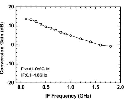
2.3 Measurement Results 0.0 0.5 1.0 1.5 2.0 -20 -10 0 10 20 IF:0.1~1.8GHz Fixed LO:6GHz C onv e rs ion G a in (dB ) IF Frequency (GHz)
Fig. 2-6 Conversion gain of the micromixer with respect to IF frequencies.
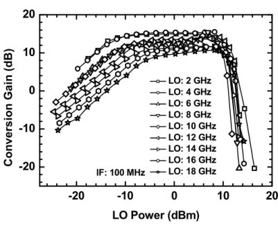
Fig. 2-7 illustrates that the effect of the LO power on the conversion gain is measured with the fixed IF frequency of 100 MHz, but different LO frequencies by Agilent’s E4448A power spectrum analyzer (PSA). The current commutation in the Gilbert cell is responsible for the frequency translation. The differential pair of the bipolar Gilbert cell only needs a small twist voltage (approximately 0.1 V) to perform the near-perfect current commutation. Once the LO power is large enough to drive the switch quad of the Gilbert mixer, the conversion gain keeps constant and is insensitive to the LO power. If the LO power is too large, the quad switch SiGe HBT transistors enter the saturation region and then the mixer gain degrades. However, there is more power to drive the switch quad at higher frequencies. With the LO frequency increase, the LO power range for the flat constant conversion gain region decreases.
Wideband Micromixer 18 -20 -10 0 10 20 -20 -10 0 10 20 C o n v e rs io n G a in (d B ) LO Power (dBm) LO: 2 GHz LO: 4 GHz LO: 6 GHz LO: 8 GHz LO: 10 GHz LO: 12 GHz LO: 14 GHz LO: 16 GHz LO: 18 GHz IF: 100 MHz
Fig. 2-7 Conversion gain of the micromixer with respect to LO power.
The RF and IF bandwidth experiments in Fig. 2-5 and Fig. 2-6 give the direct measurement of the IF and RF stage frequency response of the mixer, while the frequency response of the LO Gilbert cell is examined in Fig. 2-7. The higher the LO frequency, the narrow the flat gain region becomes. The flat gain region still exists for LO frequencies up to 18 GHz. According to the measured results, the maximum operating frequency of the mixer is approximately 15 GHz and is limited by the RF input stage.
TABLE 2.1 Measurement Results of the Wideband Micromixer TSMC 0.35m 3P3M SiGe BiCMOS Item Down-Converter RF Frequency Up to 15 GHz Conversion Gain 15 dB IF Bandwidth 400 MHz LO Speed > 18 GHz LO Power -8 dBm ~ 8 dBm RF Return Loss <-14 dB IF Return Loss < -12 dB Supply Voltage 5 V
Power Dissipation 60 mW (Core) / 65 mW (Buffer)
2.4 Summary
2.4 S
UMMARYA single-ended wideband Gilbert mixer has been demonstrated using 0.35-m SiGe BiCMOS technology. This wideband mixer has the conversion gain of 15 dB and works up to 15 GHz with 400-MHz IF bandwidth. A systematic approach to measure the frequency response of the RF, IF, and LO stages of a Gilbert mixer has been developed. The developed frequency response measurement technique can be employed to identify the frequency-limiting mechanism.
Chapter 3 Adjustable and Reactive I/Q
Generator With Constant Resistance for
Down-and Up-Converters
3.1 I
NTRODUCTIONThere is a tendency towards multimode and multiband communication systems, such as the IEEE 802.11a/b/g wireless local area network (WLAN) combo system [1]. The communication ability and diversity enhance for users but the challenges also augment for designers. For the RF integrated circuits (RFICs), it is very difficult that the optimal performance of the matching, noise figure, or quadrature accuracy is carried out for multiple frequency bands. Much research has focused on dual-band low noise amplifiers [22]. The dual-band input matching is achieved by using a high-order reactive matching network. However, generating dual-band quadrature signals from reactive elements is still a challenge.
The quadrature mechanism is widely used in the system architecture, for instance, sub-harmonic mixers [23], in-phase/quadrature (I/Q) down-converters, single-sideband (SSB) up-converters [24], and Weaver and Hartley transceivers [25]. There had been five types of quadrature generators. The first one is a polyphase filter, which is employed throughout the RFICs [26], [27]. Its phase accuracy improves with more
RC-CR sections. More than three sections are needed to resist the fabrication variation
and to maintain precise quadrature signals. However, the resistive loss of the polyphase filter also increases. Besides, the polyphase filter is not suitable at high-frequency regimes because of its parasitics and the resistor self-cutoff high-frequency [26]. Using ring oscillators to generator quadrature signals is the second means [28], [29]. Although the ring oscillators have wide oscillation frequency in comparison with L-C
Adjustable and Reactive I/Q Generator With Constant Resistance for Down- and Up-Converters
22
oscillators, their poor phase accuracy and phase noise deteriorate the performance of the entire transceiver [30]. Third, differential signals can be converted to quadrature signals by a divide-by-2 divider [31]. The input differential signals should operate with twice the desired frequency, and the oscillator with two times the desired frequency is not easily designed at high frequencies. The fourth way is to apply a quadrature coupler. The quadrature couplers, like a transmission line coupler and a Lange coupler, are often used in millimeter-wave applications [32]. However, the coupler size limits its usage in the RFICs. In spite of the size reduction of the spiral transmission line coupler, the phase accuracy and magnitude balance are not easily controlled, and hence, the performance is not good enough [33], [34].
The final solution is to directly construct a quadrature oscillator with a cross-coupling scheme between two differential oscillators. There are two types of the coupling schemes—the fundamental coupling scheme and harmonic coupling scheme. The fundamental coupling scheme includes the top-series coupling scheme, bottom-series coupling scheme, and paralleled coupling scheme [35]. There is a trade-off between phase noise and quadrature accuracy in this fundamental coupling scheme [36]. The good quadrature accuracy can be fulfilled at the cost of the phase-noise performance of the oscillators. In the harmonic coupling scheme, perfect quadrature signals can be obtained without phase noise degradation, but a differential amplifier or a transformer performing the coupling between oscillators should function at twice the oscillation frequency [37]. The quadrature ring oscillators, coupled oscillators, and dividers as quadrature generators are only employed at the LO stage.
The mentioned approaches are all utilized in a single frequency band. In this chapter, a dual band adjustable and constant-resistance I/Q generator is proposed.
3.2 Reactive I/Q Generator
Since the generator is composed of pure reactive components, inductors and capacitors, there is no loss introduced. Besides, the multiband I/Q generator is easily implemented by increasing the order of the L-C networks. Capacitors along with varactors will add the ability to control the phase and magnitude of the quadrature outputs. The configuration and optimization for the quadrature accuracy are also described here. A 2.4/5.2 GHz I/Q down-conversion mixer and a 2.4/5.7 GHz SSB upconversion mixer using 0.35-m SiGe BiCMOS are demonstrated with the dual-band adjustable and reactive I/Q generator. Thanks to the excellent quadrature accuracy, the magnitude mismatch and phase error of the down-converter outputs are <1% and <1, respectively, and the maximum sideband rejection ratio of the up-converter is up to 50 dB. According to the measurements, the down-converter outputs are always in quadrature and the I/Q generator input matching is achieved over all frequencies. In addition, the operation bandwidth (sideband rejection ratio > 30 dB) is 200 MHz at 2.4 GHz and 720 MHz at 5.7 GHz.
3.2 R
EACTIVEI/Q G
ENERATORA polyphase filter consisting of R-C and C-R sections is an I/Q generator. Nevertheless, the polyphase filter is not appropriate for high frequency applications because the parasitics and the resistor self-cutoff frequency deteriorate phase and magnitude accuracy [26]. In this dissertation, the quadrature generator formed by C-R and L-R sections is proposed here. This reactive I/Q generator is derived from the conventional C-R and R-C sections as shown in Fig. 3-1. For the R-C section, the transfer function is derived as
Adjustable and Reactive I/Q Generator With Constant Resistance for Down- and Up-Converters 24 2 1 1 1 1 R R SC R R SCR R SL R SC SC R (3.1) where 2 L CR .
Based on (3.1), the R-C section can be replaced by the L-R section as shown in Fig. 3-1. Here, a reactive I/Q generator is made of C-R and L-R sections and R is given by the input impedance of the following stage. Thanks to no extra resistive components in this reactive quadrature generator, no resistive loss would be introduced.
C
L
C
R
R
C
R
R
0
90
90
0
L
R
C
IN
V
V
A BV
Fig. 3-1 Quadrature generators with the C-R and R-C sections or with the C-R and L-R sections.
3.2.1 Wideband Reactive I/Q Generator With Constant Resistance
The reactive I/Q generator is offered here to replace the polyphase filter. The key point of design principle is that an inductor advances in phase, while a capacitor delays to result in 90 phase difference. The reactive I/Q generator is shown in Fig. 3-1. C-R and L-R are in parallel. The voltage at node A and B in Fig. 3-1 can be expressed as
3.2 Reactive I/Q Generator 1 A IN B IN R V V R j C R V V j L R (3.2)
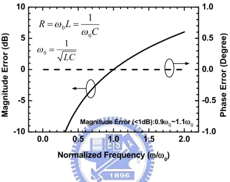
From (3.2), the reactive I/Q circuit with R=ω0L=(ω0C)-1 can generate truly balanced
quadrature signals because VAadvances for 45oand VBdelays 45owith respect to VIN.
R=ω0L=(ω0C)-1can also be viewed as R =(L/C)1/2and ω0= (LC)-1/2.
The input impedance of this generator can be written as
2 1 // 2 when in Z R j L R j C L j R R j L C C j R j L C L R R C . (3.3)Under the condition of R =(L/C)1/2, the input impedance is equal to R regardless of frequencies. If the value of R is equal to 50 Ω, the input port of the I/Q generator is wideband matched.
The voltage ratio between node A and B as a function of frequency can be expressed as 2 2 2 1 1 1 A B L R jR L V j L R C C V R R j C C . (3.4)
The voltage of node A is always quadrature to that of node B and unrelated to frequencies under the condition of R =(L/C)1/2. Also from (3.3), the input impedance is independent of frequency when R =(L/C)1/2. However, the magnitude values of both nodes are identical only at frequency of ω0. Fig. 3-2 represents the magnitude ratio
Adjustable and Reactive I/Q Generator With Constant Resistance for Down- and Up-Converters
26
ω0, when R = ω0L = 1/(ω0C). Thanks to the wideband quadrature outputs of the
reactive generator and the constant conversion gain of Gilbert mixers within a wide LO power range, mentioned in Section 2.3, the Gilbert mixers with an integrated reactive I/Q generator can work for broadband applications.
0.0 0.5 1.0 1.5 2.0 -10 -5 0 5 10 -1.0 -0.5 0.0 0.5 1.0 0 0 1 R L C
M a g n it u d e E rr o r (d B ) Normalized Frequency (/0) Magnitude Error (<1dB):0.90~1.10 0 1 LC P h a s e E rr o r (D e g re e )Fig. 3-2 Magnitude ratio ( | VA/VB| ) and phase error of the reactive I/Q generator with respect to normalized frequency ω0.
3.2.2 Dual-Band and Adjustable I/Q Generator With Constant Resistance
When compared with the polyphase filter, this reactive I/Q generator is easily designed for dual-band applications. A parallel L-C and a series L-C take place of L and C paths in the single-band I/Q generator, as shown in Fig. 3-3. The parallel L-C section is inductive at low frequencies and capacitive at high frequencies. On the other hand, the series L-C section has the opposite properties. Hence, this topology satisfies the quadrature condition at a low frequency (l) and a high frequency (h).
3.2 Reactive I/Q Generator 1 bias
DC
_ IN dualV
00
090
0
0
90
0
@ high frequency band
@ low frequency band
2
L
1L
2C
1C
R
R
_ A dualV
_ B dualV
Fig. 3-3 Topology of the dual-band I/Q generator.
The capacitor in Fig. 3-3 is in series with a varactor to add the tuning ability in the I/Q generator to conquer the fabrication variation. For simplification in the analysis, the varactors are neglected. Based on the quadrature conditions,
1 1 2 2 1 1 2 2 1 // 1 1 // 1 l l l l h h h h j L jR j C j L jR j C j L jR j C j L jR j C (3.5)
the inductance (L1 and L2) and capacitance (C1 and C2) are expressed in terms of l,
hand R as follows: 1 h l l h L R (3.6)
1 1 h l C R (3.7) 2 1 h l L R (3.8) 2 h l l h C R . (3.9)Adjustable and Reactive I/Q Generator With Constant Resistance for Down- and Up-Converters 28 _ 1 2 1 2 2 2 2 1 2 2 1 2 2 2 2 2 1 1 1 1 2 2 1 2 2 2 1 1 2 1 2 2 1 1 1 // // 1 1 1 1 1 2 1 when in dual Z R j L R j L j C j C L L C L L C R jR C L C L C C L L C R j L C C L L R R C C (3.10)
Under the condition of R = (L1/C2)1/2 = (L2/C1)1/2, the input impedance is also
equal to R regardless of frequencies and the wideband matching can be achieved [38]. The voltage ratio at node A_dual and B_dual in Fig. 3-3 can be expressed as
2 2 2 _ 2 1 _ 2 1 1 2 2 2 1 2 2 1 2 2 2 2 2 1 1 1 1 2 2 2 1 2 1 1 1 1 1 1 1 1 1 A dual B dual L C R j V C L V R j L C L L C L L C R jR C L C L C C L R L C (3.11)
and two nodes are always in quadrature regardless of frequencies when R = (L1/C2)1/2 = (L2/C1)1/2.
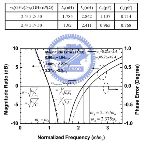
In TABLE 3.1, the ideal inductance and capacitance of the dual-band I/Q generator are calculated for WLAN applications. Here, the quadrature condition is designed based on the matching condition (R=50 Ω). The inductance and capacitance are reasonable and the dual-band I/Q generator can be realized in WLAN systems. Fig. 3-4 represents the magnitude ratio ( |VA_dual/VB_dual| ) and phase error of the dual-band
I/Q generator with respect to normalized frequency, ω0= ωl, when R = (L1/C2)1/2 =
(L1/C2)1/2. For the 2.4/5.2 GHz application, ωh= 2.167ωl and the magnitude error is
3.2 Reactive I/Q Generator
2.4/5.7 GHz application, ωh= 2.375ωl and the magnitude error is smaller than 1 dB within the 0.96–1.04 and 2.27–2.5 normalized frequency. At the transition frequency,
1 1 2 2
1 1
transition l h
L C L C
, (3.12)
the parallel L-C network (L1and C1) is open, while the series L-C network (L2and C2)
is short. All of the power flows to node B_dual. Therefore, the output magnitude ratio becomes zero and the phase reversal occurs.
TABLE 3.1 Calculated Inductance and Capacitance for Dual-Band Wi-Fi I/Q Generators.
ωl(GHz)/ωh(GHz)/R(Ω) L1(nH) L2(nH) C1(pF) C2(pF) 2.4/ 5.2/ 50 1.785 2.842 1.137 0.714 2.4/ 5.7/ 50 1.92 2.411 0.965 0.768 0 1 2 3 -10 -5 0 5 10 -1.0 -0.5 0.0 0.5 1.0 1 2 2 1 L R C L C 0 2.375 h h=5.2;l=2.4 h=5.7;l=2.4 0 l 0 2.167 h Magnitude Error (<1dB): 0.960~1.040, 2.080~2.270, 2.270~2.50 M ag n it u d e R at io (d B ) Normalized Frequency (/0) 1 1 2 2 1 1 transition l h L C L C P h as e E rr o r (D eg re e)
Fig. 3-4 Magnitude ratio ( | VA_dual/VB_dual| ) and phase error of the dual-band reactive I/Q generator with respect to normalized frequency ω0= ωl.
In comparison with a polyphase filter, there are several advantages in this reactive I/Q generator, which are listed below.
Adjustable and Reactive I/Q Generator With Constant Resistance for Down- and Up-Converters
30
high-frequency applications.
2) Zin=R, and the input matching condition is determined by the input impedance of the following circuits. Hence, it is possible to achieve the wideband matching. 3) By increasing the order of the L-C networks, it is easy to construct a multiband
quadrature generator.
3.3 C
IRCUITD
ESIGNThe proposed dual-band adjustable I/Q generator is employed at the LO stage in an I/Q down-converter and an SSB up-converter. The entire schematics of the I/Q down-converter and the SSB up-converter are depicted in Fig. 3-5 and Fig. 3-6, respectively. The mixer topology is a micromixer, which has the wideband input matching property [15], [21], [39]. Thus, the micromixer is suitable for multiband or wideband applications. The quadrature differential LO signals are generated by the dual-band reactive I/Q generator and two single-to-differential amplifiers. Here, the single-to-differential input stage of the micromixer is adopted in the single-to-differential amplifier. Thus, the input impedance of the single-to-differential amplifier also serves as the loading impedance of the I/Q generator R. The emitter followers are employed as output buffers to drive 50 Ω measurement equipments. The circuit topologies of the down- and up-converters are very similar, except the connection in the mixer outputs.
The phase property of LO signals is changed between dual bands, which alternates the quadrature property of the down-converter and the sideband property of the up-converter, as shown in Fig. 3-5 and Fig. 3-6. In the up-converter, the RF output signal of the low-frequency band is located at the upper sideband while that of the high-frequency band is located at the lower sideband.