國立交通大學
材料科學與工程研究所
碩士論文
使用陽極氧化鋁模板製造鎳奈米線於提升電解水效率
之應用
Fabrication of nickel nanowire arrays in anodic
aluminum oxide template for enhancing water
electrolysis
研究生: 陳柏均
指導教授: 吳樸偉 博士
國立交通大學
材料科學與工程研究所
碩士論文
使用陽極氧化鋁模板製造鎳奈米線於提升電解水效率
之應用
Fabrication of nickel nanowire arrays in anodic
aluminum oxide template for enhancing water
electrolysis
研究生: 陳柏均
指導教授: 吳樸偉 博士
使用陽極氧化鋁模板製造鎳奈米線於提升電解水效率上之
應用
Fabrication of nickel nanowire arrays in anodic
aluminum oxide template for enhancing water
electrolysis
學生: 陳柏均 Student: Po-Chun Chen
指導教授: 吳樸偉 博士 Advisor: Dr. Pu-Wei Wu
國立交通大學
材料科學與工程研究所
碩士論文
A Thesis
Submitted to Department of Materials Science and Engineering College of Engineering
National Chiao Tung University in partial Fulfillment of the Requirements
for the Degree of Master
in
Materials Science & Engineering June 2008
Hsinchu, Taiwan, Republic of China
I
使用陽極氧化鋁模板製造鎳奈米線於提升電解水效率
之應用
學生: 陳柏均 指導教授: 吳樸偉 博士 國立交通大學 材料科學與工程研究所 中文摘要 電解水是最簡單製造氫氣與氧氣的方式,在電解水過程減少能源的消 耗是一個重要的議題,而增加反應電極的表面積使電解水時的操作電壓降 低是其中一種方法。我們利用氧化鋁模板(AAO)製造鎳奈米線,並利用它 高深寬比的特性增加在電解水反應的有效表面積。利用直流脈衝電鍍的方 式將鎳金屬沉積至 AAO 的孔洞當中,再使用 KOH 溶液將 AAO 模板移除留下 高深寬比的鎳奈米線。在我們的研究當中製造出直徑 250 nm、長度 20~60 μm 的鎳奈米線。將鎳奈米線組成的電極使用在電解水反應當中,使用中 性及鹼性兩種電解液產生氧氣。在 0.25 M 的硫酸納當中,使用製造出來 的鎳奈米線電極作為陽極可以在 1.2 V 的電壓下產生 20 mA/cm2 的電流密 度,而以商用鎳片作為陽極則需 1.7 V 才能產生 20 mA/cm2 的電流密度。 在 1 M 的 KOH 溶液當中外加 1.8 V 電壓,鎳片作為陽極可以產生 63 mA/cm2 的電流密度。而使用鎳奈米線電極則能產生 308 mA/cm2 。在產生氫氣的反 應中,使用鹼性的 KOH 作為電解液。在外加電壓為-2 V 時,電流密度也從 使用鎳片產生的-104 mA/cm2 提高到使用鎳奈米線電極時的-388 mA/cm2 。 實驗的結果也證實鎳奈米線組成的電極可以持續工作超過 24 小時。II
Fabrication of nickel nanowire arrays in anodic
aluminum oxide template for enhancing water
electrolysis
Student: Po-Chun Chen Advisor: Dr. Pu Wei Wu
Department of Materials Science and Engineering National Chiao Tung University, Hsinchu, Taiwan ROC
Abstract
Oxygen and hydrogen both play important roles because they are the feedstocks for fuel cells. Among many production methods, the water electrolysis is the simplest one. To reduce energy consumption, the operating cell voltage should be reduced as much as possible at practical current densities. Our efforts in this area are mainly focused on the development of nickel-based electrodes because of their acceptable catalytic capabilities at reasonable material cost.
We used the direct-current (DC) pulse electrodeposition to fabricate nickel nanowires with in the AAO pore channels. After removing the AAO template by KOH solution, we obtained much larger surface areas. We fabricate nickel nanowires with lengths of 20 to 60 μm and 250 nm in diameter by adjusting the current densities in the DC pulse electrodeposition.
We used these nickel nanowires electrodes to produce oxygen in neutral and alkaline solutions, and to generate hydrogen in alkaline electrolyte. The performances for the oxygen evolution reaction (OER) and hydrogen evolution
III
reaction (HER) by using the nickel nanowires electrodes were significantly improved than that of nickel plate. Otherwise, the nickel nanowires electrodes can work continuously over one day.
IV
Table of Contents
Chapter 1. Introduction.………... 1
Chapter 2. Literature review……….…. 3
2.1.0. Anodic aluminum oxide (AAO)……….…. 3
2.2.0. Metal nanowires fabrication……….…... 4
2.2.1. Electrodeposition of metals in AAO template.…..………….. 4
2.2.2. Partial removal ofAAO template...……….. 6
2.3.0. Water electrolysis……….……...……… 7
2.3.1. Oxygen evolution reaction (OER)………..…... 7
2.3.1.1. Nickel-based electrode in alkaline electrolyte………. 8
2.3.1.2. Water electrolysis in neutral electrolyte………...…….. 11
2.3.2. Hydrogen evolution reaction (HER)………..……….. 13
Chapter 3. Experimental………..……….. 23
3.1.0. Fabrication of anodic aluminum oxide.……….…….………. 23
3.2.0. Electrode reparation for water electrolysis…..….…………... 26
3.2.1. Fabrication of nickel nanowires arrays .………. 26
3.2.2. Partial removal of AAO template…………..………. 27
3.3.0. Analysis of electrochemical properties..………….………… 28
3.3.1. Oxygen evolution reaction in neutral electrolyte...………... 28
3.3.2. Oxygen evolution reaction in alkaline electrolyte...………… 29
V
Chapter 4. Results and discussions………... 36 4.1.0. Fabrication of anodic aluminum oxide………...…. 36 4.1.10 Time determination for the pore-broadening process……….. 36 4.1.2. Influences of second-step anodizing time………….……….. 37 4.2. Fabrication of nickel arrays electrode………. 37 4.2.10. Efficiency of the pulse DC electrodeposition.……….… 38 4.2.2. Partial removal of AAO...……..……….. 39
4.3. Comparison of electrochemical measurements in neutral electrolyte.………... 41
4.3.1. Cyclic voltammetry………. 41 4.3.2. Life time of the electrode………. 42
4.4. Comparison of electrochemical measurements in alkaline electrolyte………... 42
4.4.1. Cyclic voltammetry………. 43 4.4.2. Life time of the electrode……… 43 4.5. Comparison for the hydrogen evolution reaction (HER)…… 44 4.5.1 Cyclic voltammetry………. 44 4.5.2 Life time test for the nickel nanowires cathode………... 44
4.6. Comprehensive discussions of electrocatalytic ability for water electrolysis of nickel nanowires……….... 45
4.6.1. Discussion for the electrochemical catalytic ability of the nickel nanowires………. 45
4.6.2. Comparison for nickel nanowires applied to OER and HER.. 47
VI
VII
List of Figures
Figure 2.1. Schematics for templates of (a) porous silicon, (b) porous anodic alumina, and (c) artificial opal……… 17 Figure 2.2. SEM images for anodic alumina layers in top view.
Anodization was conducted in (a) sulfuric acid at 25 V, (b) oxalic acid at 40 V, and (c) phosphoric acid at 160 V. Pore opening was carried out in 5 wt% phosphoric acid for 30 minutes. The thickness of the oxide films is approximately 120 μm……….. 18 Figure 2.3. (a)-(f) The XRD patterns for nickel nanowires fabricated
by different applied voltages, pH values, and temperatures. (a) 0.4 V, pH=2, RT. (b) 1 V, pH=2, RT. (c) 4 V, pH=2, RT. (d) 1 V, pH=2, 40 oC. (e) 1 V, pH=2, 60 oC. (f) 4 V, pH=2, 60 oC. (g) Schematic cross section (perpendicular to the substrate) of the columnar deposition. The low-surface-energy grains grow faster than do the high-energy grains. The rapid growth of the low-surface-energy gains at the expense of the high-energy grains results in an increase in grain size and favours the formation of columnar grains in the subsequent process….. 19 Figure 2.4. A schematic diagram for removal of AAO template……… 20 Figure 2.5. The pourbaix diagram for the nickel………...…….. 21 Figure 2.6. Schematic illustration of de-activation and re-generation in
VIII
preanodization at 1.5 V. (b) Formation of inert site by further oxidation of oxide at potentials higher than 1.56 V. (c) Regeneration of active site at 1.5 V………. 22 Figure 3.1. A schemetic diagram for the sample preparation………….. 31 Figure 3.2. A schematic diagram and practical cell picture of the
experimental fixtures used to fabricate AAO specimens….. 32 Figure 3.3. A schematic diagram of the holder for fixing AAO samples
during electroplating………. 33 Figure 3.4. A schematic diagram and practical cell picture for pulse
DC electrodeposition……….………... 34 Figure 3.5. The apparatus and the practical cell picture used for
electrochemical measurements... 35 Figure 4.1. The SEM images of AAO after pore-widening processing
at (a) 20, (b) 40, and (c) 60 minutes……….. 49 Figure 4.2. The top-view SEM images for the optimum broadening
process of AAO; (a) magnification in 25,000X and (b) magnification in 50,000X…...……….. 50 Figure 4.3. The cross-sectional SEM images for AAO with different
second-step anodizing times; (a) 1.5, (b) 4, and (c) 6 hr, respectively………... 51 Figure 4.4. The curve of AAO thickness vs. second-step anodizing
time………... 52 Figure 4.5. The scheme of the principle of the pulse DC
electrodeposition………... 53 Figure 4.6. The SEM images (a), (b), and EDS analysis (c) of the
IX
commercial AAO after electrodeposition of 200 mA / cm2 for 1 hour; (a) cross-sectional SEM image and (b) top-view SEM image……… 54 Figure 4.7. The SEM top-view images (a) magnification in 10,000X,
(b) magnification in 33,000X, and EDS analysis (c) of the commercial AAO after electrodeposition of 40 mA/cm2 for 1 hour………..……….. 55 Figure 4.8. The SEM top-view images (a) magnification in 5,000X,
(b) magnification in 100,000X, and EDS analysis (c) of the oxalic acid derived AAO after electrodeposition of 40 mA / cm2 for 1 hour………... 56 Figure 4.9. The SEM top-view images (a) magnification in 50,000X,
(b) magnification in 100,000X, and EDS analysis (c) of the oxalic acid derived AAO after electrodeposition of 10 mA / cm2 for 1 hour………... 57 Figure 4.10. The SEM images and EDS analysis of the nickel
nanowires after immersing in 0.5 M KOH for 45 min; (a) the upper part of the sample and (b) the bottom part of the sample………... 58 Figure 4.11. The SEM images and EDS analysis of the nickel
nanowires after immersing in 0.5 M KOH for 60 min; (a) the upper part of the sample and (b) the bottom part of the sample………... 59 Figure 4.12. The SEM images and EDS analysis of the nickel
X
the upper part of the sample and (b) the bottom part of the sample………... 60 Figure 4.13. The SEM images of sample after removing the AAO
template; top-view images in (a) magnification of 2,000X and (b) 10,000X, as well as cross-sectional images in (c) magnification of 2,000X, and (d) 5,000X…….…………... 61 Figure 4.14. The SEM images of the sample after removing the oxalic
acid derived AAO template; top-view images in (a) magnification of 10,000X and (b) 100,000X, as well as cross-sectional images in (c) magnification of 3,500X, and (d) 30,000X…..……… 62 Figure 4.15. (a) The SEM image and corresponding EDS results. (b)
and (c) are the cross-sectional images of samples after electrodeposition of 10 mA / cm2 for 30 and 60 minutes, respectively………... 63 Figure 4.16. The CV curves for the oxygen evolution reaction in 0.25
M Na2SO4……….. 64
Figure 4.17. The CV curves for oxygen evolution reaction in 1 M Na2SO4……….. 64
Figure 4.18. The CV curves in Na2SO4 electrolyte of 0.25 and 1 M (the
length of nickel nanowires is 35 μm)………..……….. 65 Figure 4.19. The galvanostatic curve for applying 50 mA/cm2 for 24
hours in 0.25 M Na2SO4……… 65
Figure 4.20. The CV curves in 1 M KOH at different temperatures with nickel nanowires of various lengths..……… 66
XI
Figure 4.21. The CV curves in KOH solutions of 0.5 and 1 M at room temperature (the length of nickel nanowires is 35 μm).…... 66 Figure 4.22. The galvanostatic curve for applying 50 mA/cm2 for 24
hours in 1 M KOH at room temperature (the length of nickel nanowires is 35 μm……… 67 Figure 4.23. The CV curves in 0.5 M KOH solution with nickel
nanowires at different lengths.……….. 67 Figure 4.24. The CV curves in 1 M KOH solution with nickel
nanowires at different lengths………... 68 Figure 4.25. The CV curves for 25 μm nickel nanowires in KOH
solutions with different concentrations………. 68 Figure 4.26. The galvanostatic curve for applying -50 mA/cm2 for 24
hours in 1 M KOH……… 69 Figure 4.27. The XRD results of (a) nickel nanowires with Pt condutive
VII
List of Tables
Table 4-1. The relationship between lengths of nanowires vs. applied current densities…..……….. 39 Table 4-2. The practical current densities of different samples………. 47 Table 4-3. The current densities for the OER and HER at
Chapter 1
Introduction
With the development of modern technologies, the general public consumes more and more energy nowadays to enjoy the conveniences those technologies bring. To date, energy crisis has become a critical issue, and everyone attempts to find alternatives for clean energy. Oxygen and hydrogen both play important roles because they are the feedstock for fuel cells, devices that provide electricity from unpolluted source. Therefore, how to produce them at reasonable cost is one of the interesting topics at present time. Conventionally, water electrolysis is one of the simplest methods for the production of oxygen and hydrogen. In order to reduce the energy consumption, the operating cell voltage should be reduced as much as possible at practical current densities. Thus, we could minimize the unit cost for electrical power consumption, since this is the primary piece of the oxygen and hydrogen production cost. For this purpose, numerous investigations have focused on the preparation of exotic electrode materials and structures. Our effort in this area is mainly focused on the development of nickel-based electrodes because of their acceptable catalytic capabilities at inexpensive material cost.
Nanowires have attracted considerable attentions due to their extraordinarily electronic, magnetic, and electrochemical properties. In particular, vertically aligned and free-standing nanowires arrays on a conductive substrate are expected to reveal higher performances in practical device applications for their excessive surface areas. The template-assisted
synthesis, such as anodic aluminum oxide (AAO) template, has been a common skeleton to prepare nanowires with high aspect ratios. Therefore, this work is geared to take advantages of the AAO for enhancing water electrolysis efficiency by producing electrodes with significant surface area. With the aid of an electroplating technique, nickel nanowires were deposited from a conductive substrate throughout the AAO pore channels. The effective surface area of the resulting electrode for water electrolysis would be increased by removing some of the AAO pore walls, exposing the nickel arrays buried within. This thesis is dedicated to develop a nickel electrode with a high surface area by careful design and fabrication of nickel arrays using AAO as a template.
Chapter 2
Literature review
Background information on anodic aluminum oxide (AAO), fabrication of nanowires, and water electrolysis are provided in this chapter.
2.1 Anodic aluminum oxide (AAO)
A template is a material with well-controlled patterns that could be used to fabricate functional devices. Many materials have been demonstrated as the templates. They include porous silicon, anodic alumina oxides, artificial opals, and polycarbonates (Fig. 2.1). In our laboratory, we are particularly interested in templates with nanochannels at high aspect ratios. We selected the AAO because it reveals well-controlled morphologies, reasonable thermal abilities, pores with high aspect ratios, dense pore densities, and superb resistances against most chemical solutions. In addition, formation of AAO involves an electrochemical method, which is a low-cost process. Thus, the AAO was chosen in this research work.
In 1995, Masuda et al. [1,2] reported a naturally self-organized nanochannel array with a densely-packed hexagonal pore structure. In AAO preparations, we obtained highly regular polycrystalline pore structures only at specific processing parameters. In contrast, amorphous pore structures with large variations could be acquired by several processing steps. Fig. 2.2 exhibits the SEM images of the AAO template fabricated by different
combinations of electrolytes and applied voltages. We observed the optimized self-organized structures at 25 V in 0.3 M sulfuric acid, 40 V in 0.3 M oxalic acid, and 195 V in 10 wt% phosphoric acid. They corresponded to AAO pore sizes of 65, 100, and 500 nm, respectively [1,2,3].
2.2 Metal nanowires fabrication
In recent years, many researches have demonstrated fabrication of metal nanowires in several ways. Methods entailing semiconductor processes [4,5,6,7,8,9,10] such as chemical vapor deposition (CVD), physical vapor deposition (PVD), laser, and focus ion beam (FIB) were employed to prepare the nanowires. However, thes approaches are typically operated under extra-high vacuum that consumes a great deal of cost and time. There are two simple and low-cost ways to fabricate metallic nanowires using AAO templates; vacuum melting injection [11] and electrodeposition. Unfortunately, the melting point of nickel is 1455 oC which is higher than the melting point of the AAO template. As a result, the vacuum melting injection could not be employed to fabricate the nickel nanowires. Hence, in our research, the electrodeposition was chosen to fabricate nickel nanowires.
2.2.1 Electrodeposition of metals in AAO template
In 2001, K. Nielsch et al. published a paper involving pulsed electrodeposition to fabricate nickel nanowires [5]. They filled the nickel into the AAO with 30 to 55 nm in pore sizes, and explored these nickel nanowires
for magnetic applications. Similarly, W. Zhang et al. reported copper/nickel nanowires fabricated by electrodeposition [12]. They successfully prepared 100 nm nanowires with the AAO template of pore channels at 100 nm.
In addition, H. Pan et al. demonstrated fabrications of nickel, silver, and zinc nanowires by controlling the applied voltages to obtain single-crystalline metallic nanowires [13]. The development of the texture or columnar structure depends on the composition, substrate, overpotential, temperature, and pH value. Thermodynamics and were used to explain the growth mechanism (Fig. 2.3), the competition between nuclei, as well as subsequent coalescence contributing to the formation of columnar structures within the nanopores of AAO. In electrodeposition processes, the surface with low-surface-energy appeared preferentially. For nickel, the surface energy followed the order of (111) > (100) > (110). The competition between the adsorption and desorption of protons at the growth surface of nickel nanowires would affect the orientation of the nanowires. This is because the protons on the working electrode could stabilize the (110) face with higher surface energy. For a higher overpotential, there appeared more protons adsorption on the cathode to form (220) preferred orientation nickel nanowires. In 2006, G. A. Gelves et al. reported that they used alternating current (AC) electroplating to successfully deposit copper into AAO [14]. They fabricated nanowires with 25 nm in diameter and 2 μm in length. They believed that the AC electrodeposition was helpful to grow copper nanowires without removing the AAO substrate.
We adopted the pulse direct current (DC) electrodeposition instead of AC or DC since we believe the former is likely to produce greater uniformity, homogeneity, and filling ratio of the nanowires within the pore channels.
Furthermore, the pulse DC electrodeposition is possible to allow for the relatively slow diffusion-driven transport in nanochannels. In addition, it was reported that the AC sinusoidal waveforms (AC electrodeposition) yielded unevenly-filled AAO pores [15]. Worst of all, the pulsed AC electrodeposition was reported to damage the AAO templates. On the contrary, the DC electrodeposition was not stable enough and the filling of AAO pores was not uniform. Therefore, we selected the pulsed DC electrodeposition to fill the AAO nanochannels in this study.
2.2.2 Partial removal of AAO template
The nanowires deposited within the AAO pore channels were highly ordered and vertically aligned. After removing the AAO template, the nanowires might maintain their mechanical stability and lodge on the conducting bottom. We could obtain more exposed areas of the nanowiwres by this way. Sander et al. [16] pointed out that the naked nanowires could be parallel to each other and normal to the surface in 2004. The schematic diagram of their experiment was shown in Fig. 2.4, and the authors obtained TiO2 nanotubes by this etching method.
Several reports documented the processes in etching the AAO template where alkaline solutions of NaOH and KOH were used [17,18]. Previously G. Song et al. determined the necessary parameters for the AAO template with pore channels of 250 nm in diameter [19]. We selected the KOH solution to etch AAO template in our experiments.
2.3 Water electrolysis
Water electrolysis is one of the primary processes for producing oxygen and hydrogen. Simple chemical reactions for water electrolysis are listed below;
2H2O ↔ O2 + 2H2 (2.1)
2H2O ↔ 4H+ + O2 + 4e- at anode (2.2)
2H2O + 2e- ↔ 2OH- + H2 at cathode (2.3)
The equation (2.1) is the overall reaction for the water electrolysis whose thermodynamic decomposition voltage is 1.229 V at standard condition. The anodic and cathodic reactions are shown in equation (2.2) and (2.3), respectively. The hydroxyl ions generated at the cathode are consumed at the anode. The oxygen evolution reaction (OER) and hydrogen evolution reaction (HER) will be demonstrated as below.
2.3.1 Oxygen evolution reaction (OER)
A possible mechanism involving several steps for the oxygen evolution was summarized by J. P. Hoare [20]. His proposed mechanisms indicated that the rate-determining step is the discharge of H2O in acid or OH- in alkaline
electrolytes:
(H2O)ads ↔ (OH)ads + H+ + e- (2.4)
(OH)ads + (OH)ads ↔ (O)ads + H2O or (OH)ads ↔ (O)ads + H+ + e- (2.5)
(O)ads + (O)ads ↔ (O2)ads and (O2)ads ↔ O2 (2.6)
the anode is likely to be the electron-transfer step (eq. 2.4 or 2.5). At a lower overpotential, the rate-determining step is shown in equation 2.4 and equation 2.5 indicates the rate-determining step at higher overpotentials.
During the process for water electrolysis, the oxygen evolution occurs on the anode. The materials for the anode are typically noble metals such as Pt, Au, Ir, Rh, and Ru. It is understood that the oxygen evolution reaction occurs on the thin oxede films on top of the metals. On some other metals (e.g., Ag, Pb, Ni), the oxygen evolution takes place on thicker layers. Among them, the nickel appeared to be the suitable electrode material for water electrolysis. Although the oxide of the nickel does not reveal the catalytic abilities comparable to those of Ru and Ir, the rising costs of the latter allow for adoption of less expensive nickel. The nickel-based electrodes which are highly corrosion-resistant and reasonable in cost were investigated earlier to improve the efficiency of water electrolysis.
2.3.1.1 Nickel-based electrode in alkaline electrolyte
Fig. 2.5 [21] provides the pourbaix diagram for nickel which offers useful insights to explain the evolutions on the nickel surfaces in water with different pH values. In alkaline water electrolysis, the nickel is chosen for electrode material. The reaction mechanism was modified as suggested by Krasil’shchilov and described below;
β–NiOOH + OH- → NiO2 + H2O + e- (E ≧ 1.8 V) (2.7)
OH- ↔ (OH)ads +e- (2.8)
2(β-NiOOH)surf + (O-)ads ↔ 2(NiO2)surf +H2O + e- (2.10)
2(NiO2)surf + (O-)ads ↔ 2(β-NiOOH)surf + (O)ads (2.11)
2(O)ads ↔ O2 (2.12)
On appropriate polarizations, the Ni(OH)2 would be oxidized to β–NiOOH,
providing the requisite active sites (Ni3+) for the oxygen evolution reaction. In addition, the β–NiOOH is partially oxidized to NiO2 which becomes inactive
for the oxygen evolution reaction (2.7). The performance for the oxygen evolution reaction on the nickel was not as good as desired, but the overpotential could be reduced by applying additional electrocatalysts or simply increasing the effective area of the electrode. The nickel oxyhydroxide (β–NiOOH) appears to be the preferred electrocatalyst for the oxygen evolution on nickel anodes. At a higher potential, the Ni3+ would oxidize to Ni4+as shown by reaction 2.7 above. Formation of NiO2 would
lower the electronic conductivity and electrochemical catalytic ability, which leads to degradation for water electrolysis. Thus, the anodization voltage should be controlled at less than 1.8 V to avoid forming NiO2 on the surface of
the nickel-based anodes [22,23,24]. In 1978, Wu et al. [23] presented their research about oxide films formed on the nickel during oxygen evolution. Fig. 2.6 illustrates a possible mechanism for the loss and regain of the electrocatalytic activities on the nickel oxide films. In their results, the significant enhancement in current densities is due to regeneration. There are three possible explanations; (i) the decrease in thickness of oxide films, and thus the reduction of resistance for the electron transfer; (ii) the alteration of microstructure of film surfaces, or more specifically, the increase of real surface area of oxide films; and (iii) the electrochemical reduction of Ni4+ to Ni3+ ion in oxide films at potentials below 1.56 V.
In order to maintain the applied voltages lower than 1.8 V, there are two practical routes to reduce the overpotentials. First, raising the operating temperature of the cell is effective in reducing the applied anodization voltage. In 1998, Bocca et al. [24] investigated the oxygen evolution reaction at 60 oC in a NaOH solution, and evaluated its current density. In their research, the authors discussed the behaviors of the nickel electrodes after different surface pretreatments. They aged the samples for 21 days to observe the changes of the electrodes with different surface pretreatments. The resulting performances were influenced considerably by transformation of Ni(OH)2 to
β-NiOOH. In 1999 [25], they replaced the anode from nickel to nickel-based alloy and kept the operating temperature at 60 oC. The electrochemical performance of the NiCo2O4 electrodes was significantly increased.
Furthermore, Ohmori et al. [26] in 2007 published their results in raising the efficiency for water electrolysis by using the integrated circuit (IC) process to fabricate the anode. They could control the thickness and porous structures by combining the nickel electrodeposition and masking process. The samples were tested in a KOH solution at different temperatures from room temperature to 80 oC. The authors implied that the performances of the anodes were adequate for water electrolysis.
Although increasing the operating temperature could improve the efficiency for water electrolysis, it consumes extra energy to maintain the cell temperature during the process for water electrolysis. An alternative way is to raise the effective surface area. In 2006, Singh et al. [27] presented their NiFe2-xCrxO4 films for the O2 evolution in a 1 M KOH solution. The
NiFe1.2Cr0.8O4 with higher surface area, in 1 M and 30 wt% KOH, were
activities. In 2007 [28], they investigated spinel-type Co3O4 and La-doped
Co3O4 in the form of thin film on nickel substrate. They indicated that small
addition of La improved the BET surface area and the apparent electrocatalytic activity of the oxide for the oxygen evolution reaction.
Another way to improve the performance of the oxygen evolution reaction is to incorporate a stable secondary cation into the nickel oxide film such as NiCo2O4 [25,27-30]. Tiwari et al. [29] investigated the active thin NiCo2O4
film on nickel to improve the oxygen evolution reaction in 1994. The oxygen overpotential on this anode film was found to be approximately 150 mV lower than that on nickel electrode [23] at 100 mA/cm2 in 1 M KOH solution at room temperature. In 1999, Bocca et al. [25] used the NiCo2O4 to obtain better
performances than those of nickel plate [24]. Hu et al. [30] presented their study about iron-nickel electrodes to evaluate the efficiency for producing oxygen. The electrochemically active surface areas were found to strongly depend on the iron content within the Fe-Ni deposits. They indicated that the Fe-Ni electrodes were suitable electrochemical catalysts for both OER and HER.
2.3.1.2 Water electrolysis in neutral electrolyte
Most of the researches for water electrolysis were investigated in alkaline electrolytes. There were relatively few documents published about water electrolysis in acid media [31] and neutral electrolyte [32,33]. In acid solutions, there was undesirable energy consumed in the corrosion processes at the nickel anode until the potential was sufficiently high enough for the O2
substantially reduced. Neutral electrolyte is another choice to carry out the water electrolysis. Earlier, Hoare [33] discussed the behavior of nickel anode in a neutral electrolyte in 1973. He investigated the electrochemical natures of nickel in NaClO3 electrolyte. In neutral electrolyte, the concentration of
OH- ions is negligible. The mechanism for water electrolysis was decomposed of H2O molecules to adsorb OH- for producing O2.
Aqueous solution of Na2SO4 is another electrolyte for the water
electrolysis [34-36]. In 1949, Bentley [34] used the Na2SO4 for water
electrolysis. T. Izumida et al. [34] used the same electrolyte to investigate electrolysis by using square-wave currents with alternative polarities. In our study, we used the Na2SO4 solution for the water electrolysis. In Na2SO4
neutral electrolyte, the reactions steps involved were (2.13)-(2.16):
2H2O ↔ O2 + 4H+ + 4e- (2.13)
4OH- ↔ O2 + 2H2O + 4e- (2.14)
OH- + H+ ↔ H2O (2.15)
SO42- + H2O ↔ HSO4- + OH- (2.16)
The electrode reactions (2.13) and (2.14) were the oxygen evolution reactions with the reactants being water and hydroxide, respectively. Reaction (2.15) was normally not affected by mass transport limitations, whereas the reaction (2.16) experienced limiting current densities due to poor supply of OH-.
Sulfate was used in the experiments which were added as Na2SO4. But in
this model it was assumed to present as SO42- and HSO4-. In the electrolyte,
the amount OH- would be increased by reducing SO42- to HSO4-. Thus, the
higher the concentrations were, the better the performances for water electrolysis were.
2.3.2 Hydrogen evolution reaction (HER)
In water electrolysis, the hydrogen evolution reaction (HER) took place on the cathode. Similarly as the oxygen evolution reaction, the nickel and nickel-based electrodes attract considerable interests to producing hydrogen.
The mechanism for the HER proceeding in alkaline solutions is shown below [37]. Reaction 2.17 presents that the water reduction with hydrogen adsorption is named Volmer step. Reaction 2.18 (Heyrovsky step) and 2.19 (Tafel step) are two parallel competitive steps; electrochemical (reaction 2.18) and chemical (reaction 2.19) desorption.
M + H2O + e- → MHads + OH- (2.17)
MHads + H2O + e- → H2 + M + OH- (2.18)
2MHads → 2M + H2 (2.19)
In this section, we introduce some methods to reduce the overpotentials during the hydrogen evolution reaction. One is evaluating operating temperature, the other is increasing effective surface area, and the last but not the least is employing a nickel-based alloy to enhance the efficiency for producing hydrogen by water elctrolysis.
First of all, raising the operating temperature of the reacting cell can diminish the applied anodization voltage. In 1995, Kibria et al. [37] used the nickel electrode for the hydrogen evolution reaction. They increased the working temperature from 28 to 77 oC in KOH solution. The nickel showed an enhanced performance with increasing temperatures, but the Tafel slope remained constant from 28 to 77 oC. In addition, they tested the duration of the electrode by applying -1.4 V at 52 oC continuously for 50 minutes without
notable current declines.
In 1995, Angelo et al. [38] used the Ni-Zn alloy electrodes to increase the surface area to improve the performance for hydrogen evolution reaction. They fabricated the alloy electrodes and used the porous nickel to increase the hydrogen adsorption, which could affect the reaction kinetics and mechanism to obtain smaller Tafel slopes. These Ni-Zn cathodes were characterized by a reduced Tafel slope 67 mV/dec.
In 1997, Šimpraga et al. [39] developed porous Ni-Fe composite electrodes to produce H2. They fabricated the Ni-Fe electrode composed by
35% Ni and 65% Fe showing much enhanced abilities for the HER. For overpotentials larger than |50| mV, the increase of currents at Ni-Fe electrodes over those at Ni was 3,500 times. The porous structure of the electrode exhibited more effective electrocatalytic activity than Ni since the adsorption behavior of the hydrogen was apparent.
In 2000, Suffredini et al. [40] improved the efficiency for water electrolysis by fabricating high-area Ni and Ni-Co coatings. They prepared Ni-Zn and Ni-Co-Zn alloy and dissolved the Zn by chemical route. This process could obtain highly porous surface with roughness factors of 2200 for Ni and 4400 for Ni-Co. The authors considered that it was possible to illustrate that only the area effect is responsible for the enhanced activity of HER. In their experiments, the cell voltage was reduced by 0.6 V as compared with others by conventional materials. A reduction of overpotential amounts to saving of electricity in water electrolysis.
In 2006, Marinovic et al. [41] investigated Ni/WC composite coatings electrode to produce hydrogen. The Ni/WC composite coatings exhibited a larger electrochemical catalyst for the HER than that of pure nickel in both acid
and based solutions. The activity for the HER was enhanced with increasing WC content in the coatings since the increasing number of active sites for the HER at the interfaces between the WC particles and nickel.
In 2007, Wei et al. [42] applied the Ni-P alloy for the hydrogen evolution reaction. They used pulse electrodeposition to fabricate the Ni-P electrode. The authors pointed out that reaction 2.17 to 2.19 are possibly the rate-control steps. At very negative potentials reaction 2.17 and 2.18 are certainly accelerated. The rate-control step for the HER would transfer to reaction 2.19 due to the hydrogen desorption from the electrode. The rate for the HER on the Ni-P is always higher than that on Ni. The author demonstrated that the strength of the Nin+1-H bond hinders the smooth desorption of hydrogen from
Ni in comparison with Ni-P. They concluded that the Ni-P alloys with P contents in a range of 9.1-14.3 at% would be suitable for all reactions mentioned below (reaction 2.17 to 2.19).
M + H2O + e- → MHads + OH- (2.17)
MHads + H2O + e- → H2 + M + OH- (2.18)
2MHads → 2M + H2 (2.19)
Ru nanorod array electrodes were also investigated by Kim et al. to enhance the performance for water eletrolysis [43]. The Ru nanorods with about 450 nm in length were deposited on the nickel substrate by a dc planar magnetron sputtering chamber. By using these Ru nanorods as the cathode for water electrolysis, the authors demonstrated approximately 25% reduction in overpotentials and 20% reduction in energy consumptions.
After reviewing these methods to reduce the overpotentails for water eletrolysis, we decided to fabricate high aspect ratio nickel nanowires to enhance the efficiency. Using electrodes with high surface area, we could
evaluate their electrocatalytic activities for oxygen and hydrogen evolution reactions.
Fig. 2.1. Schematics for templates of (a) porous silicon, (b) porous anodic alumina, and (c) artificial opal.
Fig.2.2. SEM images for anodic alumina layers in top view. Anodization was conducted in (a) sulfuric acid at 25 V, (b) oxalic acid at 40 V, and (c) phosphoric acid at 160 V. Pore opening was carried out in 5 wt% phosphoric acid for 30 minutes. The thickness of the oxide films is approximately 120 μm.
Fig. 2.3. (a)-(f) The XRD patterns for nickel nanowires fabricated by different applied voltages, pH values, and temperatures. (a) 0.4 V, pH=2, RT. (b) 1 V, pH=2, RT. (c) 4 V, pH=2, RT. (d) 1 V, pH=2, 40 oC. (e) 1 V, pH=2, 60 oC. (f) 4 V, pH=2, 60 oC. (g) Schematic cross section (perpendicular to the substrate) of the columnar deposition. The low-surface-energy grains grow faster than do the high-energy grains. The rapid growth of the low-surface-energy gains at the expense of the high-energy grains results in an increase in grain size and favours the formation of columnar grains in the subsequent process.
Fig. 2.6. Schematic illustration of de-activation and re-generation in the nickel oxide films. (a) Generation of active site by preanodization at 1.5 V. (b) Formation of inert site by further oxidation of oxide at potentials higher than 1.56 V. (c) Re-generation of active site at 1.5 V.
Chapter 3
Experimental
The entire experimental procedures are shown in Fig. 3.1.
3.1 Fabrication of anodic aluminum oxide (AAO)
The AAO template was fabricated using aluminum foil (99.7%), and the entire fabrication process took less than seven hours to complete. In general, we could produce the AAO templates with thickness from 10 to 100 μm, and pore size (diameter of each circular nanochannel) from 10 to 500 nm. The resulting aspect ratios were between 20 and 20,000. The step-by-step fabrication procedures are detailed as follows:
First of all, the aluminum foil was cleaned by acetone to remove grease from its surface followed by rinsing in distilled water and drying in open air. Afterwards, the aluminum foil was mechanically polished by pieces of water-proof SiC sandpaper to remove surface roughness. Sandpapers with decreasing average particle sizes were used consecutively to produce smoother aluminum surfaces. Next, the aluminum foil was annealed in a furnace at 600
oC under argon for 1 hour to reduce the residual stress in the foil, as well as
promote grain growth and recrystallization. Finally, the annealed sample was cleaned with pure ethanol and deionized water followed by drying out.
The annealed aluminum foil was then electropolished in a bath consisting of perchloric acid (HClO4), ethanol (C2H5OH), and monobutylether
(CH3(CH2)3OCH2CH2OH) to remove any inhomogeneities and roughness on
the surface. Two power supplies were required to provide consistent voltages. The anode was the aluminum foil, and the cathode employed was the pure platinum. Typically, fifteen minutes were required to electropolish the aluminum foil. This process enables the leveling of the aluminum foil surface since high current density areas like metal spikes could be dissolved quickly, and the remaining dirt could also be removed in this process. After the electropolishing process, the sample was rinsed with pure ethanol and deionized water again.
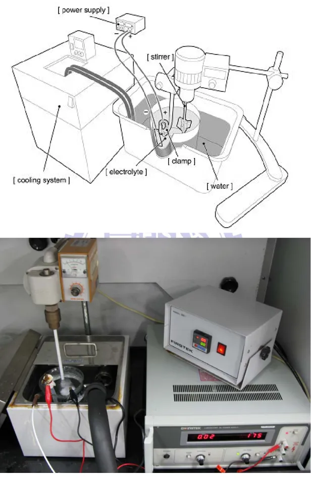
The AAO template was fabricated by anodizing the electropolished aluminum foil at 40 V in oxalic acid (C2H2O4) for 30 minutes. Fig. 3.2 is the
schematic diagrams of the experimental fixtures. Regular hexagonal arrays of pores were formed on the aluminum substrate in this simple step. Nevertheless, uniformly distributed vertically-aligned AAO template was yet to be finished after this step. The newly-formed AAO underwent a chemical removal process by immersing in a bath consisting of chromic acid (CrO3) and
phosphoric acid (H3PO4) at 60 oC for 40 minutes. Regular hexagonal arrays
of scallop-shaped indentations corresponding to the newly-formed AAO pores were produced after this operation. The formation mechanism for the AAO nanochannel structure may be explained as follows;
When we provided the voltage to the electrochemical cell composed of aluminum foil as anode and platinum as cathode, the aluminum was ionized as expected to become Al3+ simultaneously if the voltage was sufficiently high (Reaction 3.1). Also, in aqueous solution the water would be ionized to H+ and OH- (Reaction 3.2). As a result, the Al3+ was likely to associate with the OH- to form alumina (Al2O3) (Reaction 3.3). The nanochannel structure of
AAO was resulted from hydrogen (H2) escaping from the bottom of alumina
(Reaction 3.3).
Al(s) → Al3+(aq) + 3e- 3.1
H2O(l) → H+(aq) + OH-(aq) 3.2
2Al3+(aq) + 3OH-(aq) → Al2O3(s) + 1.5H2(g) 3.3
The aluminum substrate with regular patterns was subsequently anodized again to complete the second anodization of the aluminum foil. By employing this two-step anodization process, an array of ordered hexagonal cells with a cylindrical pore perpendicular to the AAO surface was obtained. Again, the AAO template was fabricated by anodizing the regular pattern bearing aluminum foil at 40 V in oxalic acid (C2H2O4) for 1 to 24 hours. We
could produce samples during various thickness by adjusting the processing time in second anodization. In other words, the longer the anodization time, the thicker the AAO template was produced. Uniformly-distributed AAO could be formed on the aluminum surface by the end of this step.
The aluminum substrate was dissolved and then removed by immersing in an aqueous bath consisting of saturated copper chloride (CuCl2) and
hydrochloric acid (HCl) for 30 minutes. The thin oxidative barrier layer, whose thickness depends on the applied voltage, was between the anodization film and aluminum substrate. This barrier layer could be removed by immersing in a phosphoric acid (H3PO4) at 25 oC for 90 minutes.
An additional chemical etching treatment could widen the nanopores by thinning the thickness of the pore channel walls. The AAO template was immersed a phosphoric acid (H3PO4) at 25 oC for different times. The pore
density and the center-to-center distance between pores remained unchanged after this operation.
The morphology of the fabricated AAO samples was observed by a field emission scanning electron microscope (FE-SEM, JEOL JSM-6500F).
3.2 Electrode reparation for water electrolysis
3.2.1 Fabrication of nickel nanowire arrays
We employed AAO templates in pore sizes of 80 nm and 250 nm. The AAO samples with 80 nm pore size were prepared according to the procedures described in section 3.1. The AAO templates with 250 nm diameter pore size were purchased from Whatman International Ltd.
The fabrication of nickel nanowire arrays was accomplished by filling the AAO nanochannels with Ni from pulse DC electrodeposition. The pulse DC electrodeposition is believed to be an effective method to deposit materials into pores of particularly high aspect-ratios.
Basically, the electrochemical deposition process is based on the cathodic reduction of metal ions dissolved in the electrolyte under an electric field. The steps are as follows;
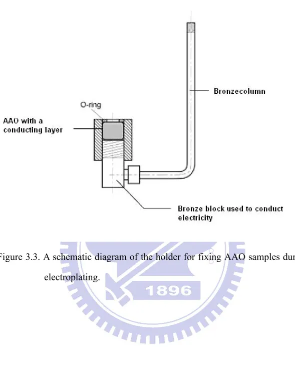
The AAO template was sputtered on its bottom surface with a thin metal film serving as a conductive layer. The template was positioned in a fixture (Fig. 3.3) to prevent the corrosive attack of acid electrolyte in the deposition process.
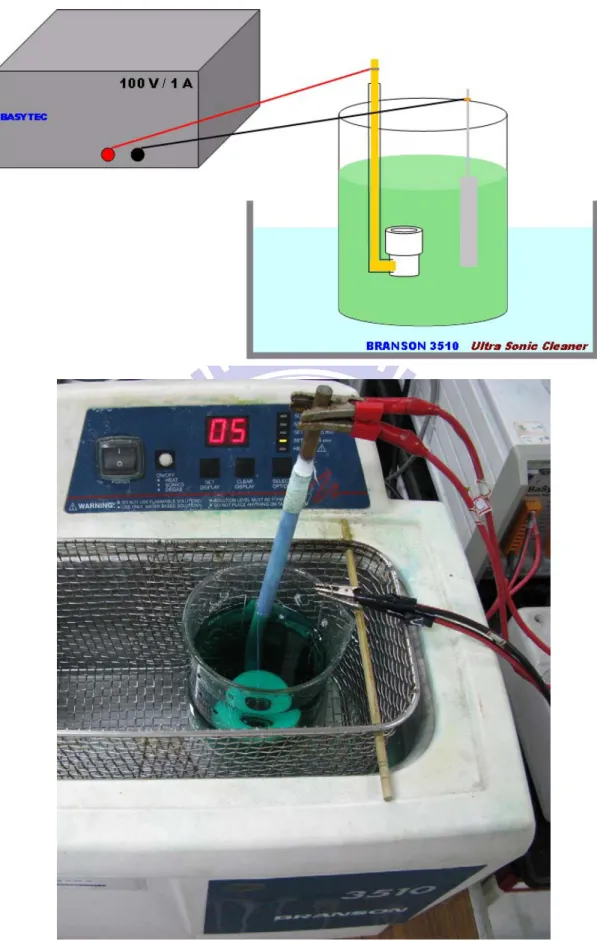
The pulse electrodeposition process was carried out in a typical two electrode electrochemical cell with the platinum as a counter electrode, and the sputtered thin conductive metal film at the bottom of AAO as a working
electrode. The practical cell picture for the pulse DC electrodeposition is shown below (Fig. 3.4). The electrolyte [44] used was a aqueous solution containing 120 g/L of NiSO4·6H2O, 60 g/L of NiCl2, 30 g/L of H3BO3, and
2g/L of PEG 2,000 (Polyethylene Glycol, used as a suppresser). The bath temperature was kept at 25 oC and the pH value was maintained at 4, respectively.
In the electrochemical deposition process, the cell was placed in an ultrasonic cleaner (Branson 3510) operated at 40 kHz to facilitate the diffusion process of metal ions into the AAO nanochannels. We expect that the metal ion depletion in the channel could be prevented by this practice. Also, the delay between pulses enables the replenishment of metal ions. The power supply was programmed to switch on and off every one second during the entire deposition period. In other words, the pulse time was 1 second, and the time period between two consecutive pulses was also 1 second. During the pulse DC electrodeposition, we adjusted different current densities to accommodate the AAO templates with different pore-sizes.
After the pulse DC electrodeposition, most AAO nanochannels were filled with the nickel nanowires. The morphologies and structures of the resulting nickel nanowires were characterized by a field emission scanning electron microscope (FE-SEM, JEOL JSM-6500F) and energy dispersive X-ray analysis (EDX), respectively. The crystal structure for the metallic nanowires was characterized by X-ray diffraction (XRD).
3.2.2 Partial Removal of AAO template
nanowires was immersed in a 0.5 M KOH solution followed by washing in deionized water. The purpose for this step was for cleaning the surface of the sample, hoping that the residual Al2O3 would be removed by the ultrasonic
cleaning. By controlling the duration of immersion time, we obtained different lengths of nickel nanowires protruding above the AAO template. The morphology and structure of the nickel nanowires were characterized by a field emission scanning electron microscope (FE-SEM, JEOL JSM-6500F) and energy dispersive X-ray analysis (EDX), respectively.
3.3 Analysis of electrochemical properties
3.3.1 Oxygen evolution reaction in neutral electrolyte
In this part, we used the sodium sulfate (Na2SO4) as electrolyte which is a
pH-neutral aqueous solution. The electrolytes with concentrations in 0.25, 0.5, and 1 M Na2SO4 were prepared at room temperature. The reference electrode
was an Ag/AgCl electrode with saturated KCl at room temperature. The cathode was a platinum plate with an area of 6.25 cm2. The anode was the nickel nanoarrays with a geometric surface area of 1 cm2 fixed by a Teflon holder (Fig. 3.3). The cell was connected to a water bath for temperature control. The experimental apparatus is shown in Fig. 3.5.
Electrochemical measurements such as cyclic voltamemetry (CV), Tafel test, and lifetime were carried out in a three-electrode arrangement using EG&G 263A. The CVs for the water electrolysis of nickel plate and nanowires were conducted in different concentrations of Na2SO4 electrolyte at
a scan rate of 50 mV.s-1 for a potential range of -0.2 to 2.0 V. The results from Tafel tests were obtained between -0.2 to 0.4 V with a scan rate of 1 mV.s-1 in electrolytes of 0.25, 0.5, and 1 M Na2SO4. The test for lifetime of
anode electrode was controlled at current density of 50 mA/cm2 by observing the voltage reading for 24 hours. All the electrochemical characterizations were conducted at room temperature with a working electrode surface of 1 cm2.
3.3.2 Oxygen evolution reaction in alkaline electrolyte
In this section, the potassium hydroxide was used as the electrolyte. Aqueous solutions of KOH in 0.5, and 1 M KOH were prepared at room temperature. The reference electrode was an Ag/AgCl electrode with a saturated KCl at room temperature. The cathode was a platinum plate with area of 6.25 cm2. The anode was fixed by a Teflon holder with a 1 cm2 geometric surface area. We employed nickel plate and nickel nanowires with different lengths as anodic electrodes. The cell was connected to a water bath for proper temperature control. The experimental apparatus is provided in Fig. 3.5.
Electrochemical measurements such as cyclic voltammetry (CV), Tafel test, and lifetime of anode electrode were carried out in a three-electrode arrangement using EG&G 263A. The CVs for the water electrolysis of nickel plate and nanowires were conducted in KOH electrolyte with different concentrations and different temperatures at a scan rate of 50 mV.s-1 for a potential range of -0.2~2.0 V. The results from the Tafel tests were obtained between 0.4 to 0.8 V with a scan rate of 1 mV.s-1 in aqueous electrolytes of 0.5 and 1 M KOH. The test for lifetime of anode electrode was controlled at a
current density of 100 mA/cm2, and we monitored the supply voltage for reading 10 hours. All the electrochemical characterizations were conducted at room temperature and 50 oC with a working electrode surface of 1 cm2.
3.3.3 Hydrogen evolution reaction in alkaline electrolyte
In this section, the potassium hydroxide was used as the electrolyte. Aqueous solutions of 0.5, 1, and 5 M KOH were prepared at room temperature. The reference electrode was an Ag/AgCl electrode with a saturated KCl at room temperature. The cathode was platinum plate with an area of 6.25 cm2. The anode was fixed by a Teflon holder with a 1cm2 geometric surface area. We used nickel plate and nickel nanowires with different lengths as anodic electrodes. The cell was connected to a water bath for temperature control. The experimental apparatus is provided in Fig. 3.5.
Electrochemical measurements such as cyclic voltammetry (CV), Tafel test, and lifetime of anode electrode were carried out in a three-electrode arrangement using EG&G 263A. The CVs for the water electrolysis of nickel plate and nanowires were conducted in KOH electrolyte with different concentrations and at different temperatures at a scan rate of 50 mV.s-1 for a potential range of -0.2 to -2.0 V. The results from the Tafel tests were obtained between -1.3 to 0.7 V with a scan rate of 1 mV.s-1 in electrolytes of 0.5 and 1 M KOH solutions.
Figure 3.1. A schematic diagram for the sample preparation.
Fabricate anodic aluminum oxide (AAO) in various sizes
Sputter platinum as conducting layer
Electroplating nickel into AAO template
Characterization of nickel nanorods by SEM, XRD, and EDX
Electrochemical measurements by CV and Tafel Remove partial AAO template
Figure 3.2. A schematic diagram and practical cell picture of the experimental fixtures used to fabricate AAO specimens.
Figure 3.3. A schematic diagram of the holder for fixing AAO samples during electroplating.
Figure 3.4. A schematic diagram and practical cell picture for pulse DC electrodeposition.
Figure 3.5. The apparatus and the practical cell picture used for electrochemical measurements.
Chapter4
Results and discussion
4.1 Comparison of Fabrication of Anodic Aluminum Oxide
In order to obtain desirable nanoporous structures on the AAO, many processing parameters should be carefully controlled. They include anodic voltages, electrolyte compositions, temperatures, stirrings, and current densities. If the fabrication process was not conducted properly, specific nanoporous structures could not be obtained. Therefore, for the purpose of reducing the variations in results, we only varied variables of anodization voltage and pore widening parameters.
4.1.1 Time selection for the pore-broadening process
In our typical processing protocol, the sample was immersed in 3 wt% C2H2O4 of 40 V at 25oC with constant stirring in the electrolyte. The only
variation was the duration in 5 wt% H3PO4 used as the pore-widening
electrolyte. Fig. 4.1 provides the SEM images of pore-broadening process at various times.
When the duration was 20 minutes, the pore size was not large enough. The walls of pore channels were thicker than the pore diameters, and they could be widened further to obtain better nanochannels. After prolonging the pore-widening to 60 minutes, we arrived at a situation of over-widening in which the pores were connected to each other with presence of large holes or L-shape nanochennels. At this moment, the AAO film was not useable
anymore. The original pore size was relatively narrow as shown in the image of AAO prior to the broadening. After broadening, the pore size was equal to the thickness of pore wall or even thicker. Samples after proper broadening treatments demonstrated uniformity pore channels, which could be used for following electrodeposition.
4.1.2 Influences of second-step anodizing time
After exploring the anodizing times from 1 to 30 hours we obtained AAO in distinct morphologies as shown in Fig. 4.2 and 4.3. According to the scale bar in Fig. 4.2, the optimized process produced AAO with pore diameter about 80 nm and density of approximately 1010/ cm2.
Fig. 4.3 exhibits the cross-sectional views of AAO with different anodizing times from 1.5 to 6 hours. The growth evolution of the AAO film thickness followed a parabolic curve with increase of anodization time. In the beginning, the thickness of AAO grew rapidly followed by steady reduction in the growth rate. As a result, when the anodizing time was longer than 10 hours, the efficiency of anodizing treatment became compromised. Fig. 4.4 presents the relation of AAO thickness vs. anodizing time.
4.2 Comparison of Fabrication of Nickel Arrays Electrode
The fabrication of nickel nanowire arrays was accomplished by filling the AAO pore channels with Ni from the pulse DC electrodeposition. The pulse DC electrodeposition is believed to be an effective method to deposit materials
into pores of particularly high aspect-ratios. Fig. 4.5 illustrates the fabrication scheme for the pulse DC electrodeposition. In an ideal case, the Ni2+ ion would diffuse into the pore channels and be reduced to Ni atom on the conductive layer when sufficient voltage was imposed.
Ni2+ (aq) + 2e- → Ni(s) Eo = 0.257 V
However, in practical case the substrate with nano channels might not obey the typical mechanism of electrodeposition. Because factors such as diffusion of Ni2+ ions into pore channels and aspect-ratios of the pore channels were critical.
4.2.1 Efficiency of the pulse DC electrodeposition
The efficiency for the pulse DC electrodeposition was discussed in this section. We explored various current densities and electroplating times to identify the optimized conditions for the pulse DC electrodeposition. Fig. 4.6 exhibits the SEM top-view images (a), (b), as well as EDS analysis (c) of the commercial AAO. The current density was 200 mA /cm2 with duration of 1 hour. The pores were obstructed by nickel particles and EDS analysis confirmed that there was no nickel deposited in the upper AAO. Thus, we reduced the current density to 40 mA /cm2, and maintained the duration for 1 hour. The SEM top-view images (a), (b), and EDS analysis (c) of the commercial AAO are shown in Fig. 4.7. As clearly presented in fig. 4.7(a), about 90 % pores were filled by nickel nanowires. In addition, we observed nickel nanowires in the upper AAO from the EDS analysis. Because of the metallic ions accumulated at top of the AAO particularly at higher current densities, the metallic ions could be the nucleation sites to form nickel particles
on the surface before embedding nickel into the nano-pores of the AAO. Table 4-1 lists relationship for the length of nickel nanowires vs. deposition time with a current density of 40 mA /cm2.
Table 4-1: The relationship between lengths of nanowires vs. applied current densities.
Deposition time = 1 hour
Current density (mA) 20 25 30 35 40
Length (μm) 20 32 43 50 60
When we attempted to deposit the nickel into oxalic acid derived AAO whose pore channels were 70 μm, the undesirable nickel ion accumulation was more obvious. The SEM top-view images (a), (b), and EDS analysis (c) of the oxalic acid derived AAO are shown in Fig. 4.8. We determined that it was difficult to fill nickel into the nanpores with a current density of 50 mA/cm2. Because the pore size of oxalic acid derived AAO was 80 nm, metallic ions were more difficult to diffuse into the nanochannels. Thus, we should reduce the current density to acquire desirable filling of AAO by nickel nanowires. Fig. 4.9 shows the SEM top-view images (a), (b), and EDS analysis (c) with a current density of 10 mA/cm2 for 2 hours. There was over 90 % nanopores filled by nickel nanowires.
4.2.2 Removal of partial AAO
In this section, we discuss the results of removing AAO partially. After we immersed the AAO template deposited with nickel nanowires into 0.5 M
KOH aqueous solution, the aluminum oxide was dissolved by the strong alkaline electrolyte.
Fig. 4.10 presents the SEM cross-sectional images and EDS analysis results. Fig. 4.10(a) and (b) are the samples with a current density 30 mA/cm2 for 1 hour followed by immersion into 0.5 M KOH for 45 min. The length of the nickel nanowires was about 40 μm. After immersing the sample into 0.5 M KOH, there was residual undissolved AAO whose thickness was about 20 μm. Alternatively, the sample was immersed into 0.5 M KOH for 60 minutes, and the resulting thickness for the remaining AAO was about 10 μm. (Fig. 4.11) Fig. 4.12 presents the sample which was immersed into 0.5 M KOH solution for 80 minutes. We did not observe the aluminum peak from the EDS analysis. This result indicated that all the remaining AAO template was removed. Fig. 4.13 shows the SEM of the nickel nanowires. After the sample was immersed in 0.5 M KOH solution for 80 minutes, the AAO template was completely dissolved. However, there were numerous bundles of nickel nanowires in the SEM top-view image (Fig. 4.13(a) and (b)). These free-standing nickel nanowires were supported by the conducting layer at the bottom of the substrate. We surmise that the static charges among these nickel nanowires are responsible for the observed bundle formations. In Fig. 4.13(c), the length of the nickel nanowires was 36 μm after applying 28 mA/cm2 for 1 hour. In addition, there was negligible residual AAO in Fig. 4.13(d).
Fig. 4.14 exhibits the SEM top-view images for the nickel nanowires with diameter of 80 nm. After immersing the samples into 0.5 M KOH solution for 30 minutes at room temperature, the AAO template with thickness of 25 μm was entirely dissolved. The SEM cross-sectional images and results of EDS
analysis are provided in Fig.4.15. The cross-sectional images revealed that the lengths of the nickel nanowires were 5 and 20 μm with different deposition times. The EDS results confirmed there was negligible residual AAO at the bottom of the sample.
4.3 Comparison of Electrochemical Measurements in
Neutral Electrolyte
In this section, we discuss the electrochemical characteristics of the electrodes with nickel nanowires array in neutral electrolyte. The AAO templates for the electrode fabrications were in two different pore sizes. We applied 28 mA/cm2 for 1 hour to the AAO with 250 nm in pore sizes. In contrast, the AAO with 80 nm nanopores was subjected to current density of 10 mA/cm2 for 1hour. The lengths of the nickel nanowires were controlled by adjusting the current densities for electrodeposition. The duration for electrodeposition was maintained for 1 hour.
4.3.1 Cyclic voltammetry
Cyclic voltammograms were conducted at room temperature in 0.25 and 1 M Na2SO4 aqueous solutions on different nickel electrodes. Fig. 4.16
demonstrated the CV curve in 0.25 M Na2SO4 electrolyte. The nickel
nanowires samples were tested in this experiment with 250 nm pore sizes. We obtained higher current density with longer exposed nickel nanowires. The CV curves in 1 M Na2SO4 was shown in Fig. 4.17. We employed two kinds
of AAO with 80 and 250 nm in diameters, respectively.
Fig. 4.18 presents the CV curve in Na2SO4 electrolyte solution with
different concentrations. The results indicated that we could obtain higher current densities in more concentrated Na2SO4 electrolyte. We mentioned the
reacting mechanism for the water electrolysis in Na2SO4 electrolyte previously
in chapter 2 (SO42- + H2O ↔ HSO4- + OH-). There is likely to have more
hydroxide ions in the electrolyte by increasing the SO42- concentration.
4.3.2 Life time of the electrode
After applying 50 mA/cm2 for 24 hours in 0.25 M Na2SO4 electrolyte, the
E-t curve is shown in Fig. 4.19. At the beginning of the life time measurement, the voltage was about 1.65 V. We could observe that the voltage at 50 mA/cm2 was still lower than 1.7 V. The result implied that the electrode we made could be used to produce oxygen at relatively lower voltage continuously for a day.
4.4 Comparison of Electrochemical Measurement in
Alkaline Electrolyte
Water electrolysis conducted in alkaline electrolyte is discussed in this section. The results for electrochemical measurements are provided below. Again, we adjusted the etching time to control the exposed lengths of nickel nanowires.
4.4.1 Cyclic voltammetry
Cyclic voltammograms were obtained in 0.5 and 1 M KOH solutions at room temperature and 50 oC on the different nickel electrodes.
Fig. 4.20 provides the CV curves in 1 M KOH electrolyte at different temperatures, from room temperature to 50 oC, respectively. The nickel nanowires samples were tested in this experiment with 250 nm in diameter. The lengths of the samples we prepared were 30 and 35 μm, respectively. We acquired higher current densities at higher temperatures. In addition, the current densities were higher with longer nickel nanowires at room temperature, but the current densities were unchanged with respect to lengths at 50 oC. It was because the residual AAO in the samples were dissolved in KOH at 50 oC rather quickly, and so the exposed nickel nanowires remained constant. This behavior was not observed at room temperature because the etching rate was much slower.
The CV curves in KOH electrolyte with different concentrations at room temperature are shown in Fig. 4.21. The current density recorded was higher in 1 M KOH electrolyte than that in 0.5 M KOH solution. There were more hydroxide ions in the 1 M KOH electrolyte, and these ions were beneficial for the oxygen evolution reaction.
4.4.2 Life time of the electrode
After applying 50 mA/cm2 for 24 hours in 1 M KOH, the resulting E-t curves are presented in Fig. 4.22. At the beginning of the life time measurement, the voltage was about 0.8 V. We observed that the voltage at 50
mA/cm2 was still lower than that of 0.9 V which was an acceptable voltage to produce oxygen. The result implied that the electrode we made could be used continuously with 50 mA / cm2 for a day.
4.5 Comparison for the hydrogen evolution reaction (HER)
4.5.1 Cyclic voltammetry
Cyclic voltammograms were obtained in 0.5 and 1 M KOH solutions at room temperature on different nickel electrodes. Fig. 4.23 presents the results of CV tests in 0.5 M KOH solution. Fig. 4.24 demonstrates the CV curves in 1 M KOH solution. Higher current densities were obtained with samples of longer nickel nanowires in both KOH electrolyte solutions. Furthermore, Fig. 4.25 presents the CV results for the hydrogen evolution reaction in 0.5, 1, and 5 M KOH solutions with nickel nanowires of 25 μm length. The results indicated that the nickel nanowires produced more hydrogen in KOH solution with higher concentrations.
4.5.2 Life time test for the nickel nanowires cathode
After applying -50 mA/cm2 for 24 hours in 1 M KOH, the resulting E-t curves are presented in Fig. 4.25. At the beginning, the voltage was about -1.25 V. We observed that the voltage at -50 mA/cm2 was still larger than -1.3 V for 24 hours. This result implied that the electrode we made could be used continuously at -50 mA / cm2 current density without notable degradation.
4.6 Comprehensive discussions of electrocatalytic ability for
water electrolysis of nickel nanowires
4.6.1 Discussion for the electrochemical catalytic ability of the nickel
nanowires
A general trend was observed for samples in different electrolyte concentrations and types of electrolytes. Nickel nanowires with longer lengths produced highest current densities. We believe the effective electrochemical surface area is the critical element in the resulting current. We could estimate the surface area by the equation below;
A =ρ × (π × γ2
+ 2πγ × ι) ρ: the amount of the nickel nanowires in 1 cm2 γ: the radius of the nickel nanowires
ι: the length of the nickel nanowires
Following the equation listed above, we obtained the practical surface area of the AAO with different pore sizes. In commercial AAO template, there were 1.6 × 10⁹ nickel nanowires per cm2. If we exposed 1 μm nickel nanowires, the practical surface area arrived at 13.3 cm2. We could derive the relationship of the practical surface area with the length of exposing nickel nanowires as below;
A = 5.03 × (0.16 + 2.5 × ι)
In the oxalic acid derived AAO, there were 1.2 × 10¹⁰ nickel nanowires per cm2. If we exposed 1 μm nickel nanowires, the practical surface area amounted to 30.8 cm2. We presented the relationship for the practical surface
area with the length of exposing nickel nanowires as below; A = 3.78 × (0.16 + 8 × ι)
By these calculations, we determined that the practical surface area for the oxalic acid derived AAO was larger than that of commercial AAO per μm length. Unfortunately, the process of removing oxalic acid derived AAO partially still presented some technical problems to overcome. We could not remove all oxalic acid driven AAO template like commercial AAO. Thus, the efficiency for commercial AAO was better than that of oxalic derived AAO at this moment (Fig. 4.17).
Taking Fig. 4.16 for an example, we could observe the current density of nickel nanowires anode. The surface areas for the anodic electrodes were 267, 333, and 467 cm2, respectively. But the current densities at 2 V were less than 10 times of the nickel plate with 1 cm2 surface area. Furthermore, Table 4-2 lists the practical current densities for the samples with different practical surface areas at 1.8 V in 1 M KOH electrolyte at room temperature. We observed that the practical current density for nickel plate was over 60 times to nickel nanowires. There were two possible explanations as mentioned below;
Table 4-2: The practical current densities of different samples at 1.8 V.
Nickel plate 25 μm length 30 μm length 35 μm length
Real surface area (cm2) 1 267 333 467
Current density (A / cm2) 0.0633 0.264 0.287 0.308
Practical current density (A / cm2) 0.0633 0.000989 0.000862 0.000659
First of all, in the SEM image (Fig. 4.13 (a)) we observed that there were many nickel bundles after removing the AAO template. This phenomenon might explain reduction of the surface area since the nearby nickel nanowires were touching each others. Secondly, the electrochemical catalytic ability for the nickel nanowires was worse than that of the nickel plate. The results were likely due to the difference in the preferred orientation between the nickel nanowires and nickel plate. Fig. 4.27 provides the XRD results for nickel nanowires and nickel plate, which indicate (111) preferred orientation for the nickel nanowires, and (200) prefer orientation by nickel plate. According to literature, the (220) plane revealed better electrochemical catalytic abilities [45]. This satisfactorially explains why the samples we made could not exhibit the anticipated performances to our desire.
4.6.2. Comparison for nickel nanowires applied to OER and HER
The E0 were obtained by the Tafel test. The E0 of the OER and the HER for the nickel nanowires in KOH electrolyte solutions were 0.57 and -0.98 V, respectively. Fig. 4.28 exhibts the I-V curves of the OER and HER in 0.5 and 1 M KOH solutions. The current densities at 1.0 V of overpotential are indicated in Table 4-3. The current densities of the nickel nanowires for the