Tungsten oxide/tungsten nanocrystals for nonvolatile memory devices
C. H. Chen, T. C. Chang, I. H. Liao, P. B. Xi, Joe Hsieh, Jason Chen, Tensor Huang, S. M. Sze, U. S. Chen, and J. R. Chen
Citation: Applied Physics Letters 92, 013114 (2008); doi: 10.1063/1.2822401 View online: http://dx.doi.org/10.1063/1.2822401
View Table of Contents: http://scitation.aip.org/content/aip/journal/apl/92/1?ver=pdfcov Published by the AIP Publishing
Articles you may be interested in
NiSiGe nanocrystals for nonvolatile memory devices Appl. Phys. Lett. 94, 062102 (2009); 10.1063/1.3080201
Nonvolatile memory devices with high density ruthenium nanocrystals Appl. Phys. Lett. 93, 242102 (2008); 10.1063/1.3049598
Tungsten nanocrystal memory devices improved by supercritical fluid treatment Appl. Phys. Lett. 91, 232104 (2007); 10.1063/1.2803937
Minimization of germanium penetration, nanocrystal formation, charge storage, and retention in a trilayer memory structure with silicon nitride/hafnium dioxide stack as the tunnel dielectric
Appl. Phys. Lett. 84, 4385 (2004); 10.1063/1.1757022
Effect of germanium concentration and tunnel oxide thickness on nanocrystal formation and charge storage/retention characteristics of a trilayer memory structure
Appl. Phys. Lett. 83, 3558 (2003); 10.1063/1.1615840
This article is copyrighted as indicated in the article. Reuse of AIP content is subject to the terms at: http://scitation.aip.org/termsconditions. Downloaded to IP: 140.113.38.11 On: Wed, 30 Apr 2014 08:41:21
Tungsten oxide/tungsten nanocrystals for nonvolatile memory devices
C. H. Chen
Department of Materials Science and Engineering, National Tsing Hua University, Hsinchu, Taiwan 300, Republic of China
T. C. Changa兲
Department of Physics and Institute of Electro-Optical Engineering, and Center for Nanoscience and Nanotechnology, National Sun Yat-Sen University, Kaohsiung, 804 Taiwan, Republic of China I. H. Liao
ProMOS Technologies, No. 19, Li Hsin Rd., Science-Based Industrial Park, Hsinchu, Taiwan 300, Republic of China
P. B. Xi
Institute of Electro-Optical Engineering, National Sun Yat-Sen University, Kaohsiung, Taiwan 804, Republic of China
Joe Hsieh, Jason Chen, and Tensor Huang
ProMOS Technologies, No. 19, Li Hsin Rd., Science-Based Industrial Park, Hsinchu, Taiwan 300, Republic of China
S. M. Sze
Institute of Electronics, National Chiao Tung University, Taiwan, Hsinchu, Taiwan 300, Republic of China U. S. Chen and J. R. Chen
Department of Materials Science and Engineering, National Tsing Hua University, Hsinchu, Taiwan 300, Republic of China
共Received 13 July 2007; accepted 16 November 2007; published online 7 January 2008兲
In this work, the fabrication of WO3/W nanocrystals for nonvolatile memory devices has been
achieved via rapid thermal oxidation of tungsten silicide. Amorphous Si and WSix共x=2.7兲 layers
were deposited onto the tunneling oxide and sequentially oxidized to form well-shaped WO3/W
nanocrystals. The mean size of WO3/W nanocrystals is ⬃8.4 nm, while density is ⬃1.57
⫻1011cm−2. Moreover, the nonvolatile memory device for WO
3/W nanocrystals exhibits ⬃0.53 V
threshold voltage shift under 1 V/共−5 V兲 operation. The sample without capping a-Si layer was also fabricated for comparison. By material analyses, reasonable formation mechanisms are proposed in this letter. © 2008 American Institute of Physics. 关DOI:10.1063/1.2822401兴
In recent years, extensive articles have been published relating with nanocrystal application on nonvolatile memory devices. The memory devices employing distributed nano-crystals as storage elements have exhibited outstanding per-formance in high speed and low power consumption so that it has been regarded as a candidate to replace conventional dynamic random array memories and/or flash memories.1–3 Theoretically, metal nanocrystals possess more advantages than other materials for nonvolatile memory devices, such as a wide range of available work functions, higher density of states, and smaller energy perturbation due to carrier confinement.4–6However, few metal materials could be em-ployed in manufacture of current semiconductor industry be-cause of incompatibilities with various processes. Among the practicable metals for semiconductor industry, tungsten pro-vides excellent physical as well as electrical properties for satisfaction of both requirements. For example, high melting point prevents deformation at high temperature, high work function provides high density of states for electrons trap-ping, chemical stability with Si atom, and so on.7,8
In this letter, the fabrication of well-shaped WO3/W nanocrystals embedded in SiO2 for nonvolatile memory
de-vice application has been demonstrated. Additionally, the failure mechanism of imperfect WO3/W nanocrystal-based
nonvolatile memory without capping a-Si layer is discussed as well.
8 in. 共100兲 oriented p-type silicon wafers were chemi-cally cleaned by a standard RCA procedure, followed a 3 nm tunnel oxide was grown in a rapid thermal anneal system. Subsequently, a 4-nm-thick WSix 共x=2.7兲 layer was
depos-ited onto the tunnel oxide using chemical vapor deposition system. An amorphous Si layer 共a-Si, 5 nm兲 was capped onto the tungsten silicide layer to provide sufficient Si atoms for forming the control oxide layer. Afterward, a dry oxida-tion was utilized for the formaoxida-tion of the control oxide at 900– 1100 ° C and WO3/W nanocrystals were precipitated in the matrix of SiO2as well. In addition, the sample without
capping a-Si layer was also oxidized in the same conditions. Chemical compositions of samples were investigated by x-ray photoelectron spectrometry共XPS兲 共Physical Electron-ics PHI 1600兲 with Mg K␣ 共energy=1253.6 eV兲 radiation. Finally, Al gate electrode was patterned and sintered. The structural analyses were performed by transmission electron microscopy共TEM兲. The capacitance-voltage 共C-V兲 measure-ments were performed by a precision LCR meter共HP4284A兲 to observe the memory characteristics of WO3/W
nanocrystal-based devices.
Figure 1共a兲 shows the cross-sectional TEM image of WSix/SiO2/Si structure for RTO process. An about 150 nm
cluster was observed on the tunneling oxide. The clusters
a兲Electronic mail: [email protected].
APPLIED PHYSICS LETTERS 92, 013114共2008兲
0003-6951/2008/92共1兲/013114/3/$23.00 92, 013114-1 © 2008 American Institute of Physics
This article is copyrighted as indicated in the article. Reuse of AIP content is subject to the terms at: http://scitation.aip.org/termsconditions. Downloaded to IP: 140.113.38.11 On: Wed, 30 Apr 2014 08:41:21
appear repeatedly on the sample every several micrometers. Besides, the dark contrast in TEM suggests that it was com-posed of tungsten and/or tungsten compounds. The square shows a highlighted high-resolution TEM 共HRTEM兲 image from the Fig.1共a兲. WO3/W nanocrystals are conspicuously
observed embedded in SiO2 matrix, while the nanocrystals
are segregated imperfectly in shape.
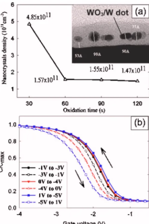
In order to improve the formation of imperfect-shaped nanocrystals aforementioned, a 5 nm a-Si layer was capped on WSix layer and followed oxidizing in the same
condi-tions. The inset of Fig.2共a兲represents the HRTEM image of oxidized a-Si/WSix/SiO2/Si structure. It displays that the
WO3/W nanocrystals were formed into distributed- and
well-shaped ellipsoids. The confirmation of mean size of WO3/W nanocrystals is approximately 8.4 nm in diameter. Figure2共a兲shows the density of WO3/W nanocrystals
ver-sus rapid thermal oxidation 共RTO兲 time. At initially 30 s, WO3/W nanocrystals nucleated rapidly and sequentially
coarsened. As RTO performed at 60 s, the density of WO3/W nanocrystals decreases to 1.57⫻1011 cm−2, and
there is no obvious variation from 60 to 120 s. The C-V characteristics of WO3/W nanocrystals embedded in oxide
are shown in Fig.2共b兲. While the voltage swept from 1 to − 5 V and back to 1 V, a threshold-voltage shift of 0.53 V was observed, which is sufficient to be defined as “1” or “0” for the logic-circuit design.
XPS was used to determine the chemical nature of the
a-Si/WSix/SiO2/Si sample which was oxidized for 120 s
RTO process. Ar sputtering for 100 sec is utilized for clean-ing. Figure 3 presents the XPS spectra of W 4f. The peaks centered at 3.14 and 33.4 eV were identified as W 4f7/2and W 4f5/2, respectively. Slight WO3 chemical states were
ob-served at 35.8 and 37.8 eV as well.9Nevertheless, Si atoms in the sample are mostly oxidized, which the evidence is SiO2 signal identified from Si 2p XPS spectra. Because of
extremely little solid solubility of O atoms within W
material,10O atoms could not exist in W nanocrystals except absolutely oxidation of tungsten. Therefore, it is a reasonable speculation that the position of WO3 should be on the
sur-face of W nanocrystals. Namely, W nanocrystals are encap-sulated by a very thin WO3layer.
To elucidate the appearance of samples with and without
a-Si layer, a schematic diagram is shown in Fig.4. Initially, tungsten silicide is oxidized and decomposes to W and Si.11,12 Both elements transform to oxygen compounds si-multaneously. Comparing with the oxides of W and Si, the heats of formation per oxygen atom are −67.1 kcal/mole for WO3 and −73.0 kcal/mole for SiO2, respectively.7It is
rea-sonable to believe that the primitive oxidation mostly arises with Si atoms, and only slight W atoms are transformed into W oxides.13 At the same time, tungsten also aggregates to diminish free energy of surface. However, WO3is not stable
at high temperature. Some WO3vaporized during the
nucle-FIG. 1.共a兲 Cross-section TEM micrograph of WSix/SiO2/Si structure for
rapid thermal oxidation treatment and共b兲 locally magnifying image from Fig.1共a兲
FIG. 2.共Color online兲 共a兲 The variation of WO3/W nanocrystals density vs
RTO process time. The inset is the cross-section TEM micrograph of
a-Si/WSix/SiO2/Si structure for RTO treatment. 共b兲 The
capacitance-voltage共C-V兲 hysteresis of WO3/W nanocrystals memory device after bi-directional sweeps between共−1 V兲/共−3 V兲, 0 V/共−4 V兲, and 1 V/共−5 V兲.
FIG. 3.共Color online兲 The W 4f XPS spectra of a-Si/WSix/SiO2/Si sample
for RTO process. The sample was performed after 100 s Ar sputtering.
013114-2 Chen et al. Appl. Phys. Lett. 92, 013114共2008兲
This article is copyrighted as indicated in the article. Reuse of AIP content is subject to the terms at: http://scitation.aip.org/termsconditions. Downloaded to IP: 140.113.38.11 On: Wed, 30 Apr 2014 08:41:21
ation, thus the imperfect shape of WO3/W nanocrystals
formed, as shown from Fig.4共a兲to Fig.4共c兲. It is confirmed in Fig.1共b兲. Furthermore, difference thermal expansion co-efficients are induced between the tunneling oxide and W silicide共0.5 ppm/ °C for SiO2 and 12.5 ppm/ °C for WSi2兲. W silicide film is compressed by thermal stress during ther-mal oxidation process. The stress attributes to enhance the aggregation of the WO3/W and results in clustered, as
shown in Fig.1共a兲.
Because the cluster formation is due to raising a violent thermal stress in a W silicide film during oxidation, WO3/W
nanocrystals must be precipitated before the W silicide film reacts with oxygen to alleviate the cluster formation. Cap-ping an a-Si layer on W silicide film, as shown in Fig.4共d兲, is a significant way to retard oxygen diffusing into the W silicide film. First, an upper a-Si layer is beneficial to reduce the formation of stress at high temperature. Moreover, great parts of SiO2are transformed from a-Si capping layer during
oxidation. Oxide layer also moderates the diffusion of oxy-gen into W silicide. The delay time of the W oxidation makes the decomposed W atoms to aggregate completely, as shown in Fig.4共e兲. Even if tungsten is slightly oxidized, the thin SiO2layer also plays a significant role in keeping WO3from evaporation. Capping a-Si layer onto W silicide before oxi-dation indeed results in perfect shape of WO3/W
nanocrys-tals.
In summary, the fabrication of WO3/W nanocrystals as
memory devices by oxidizing a-Si/WSix/SiO2/Si structure
has been achieved. The nonvolatile memory device with WO3/W nanocrystals exhibits ⬃0.53 V threshold voltage
shift under 1 V/共−5 V兲 operation. Meanwhile, the mecha-nisms of formation of WO3/W nanocrystals also are
pro-posed. Volatile WO3and excessive stress lead to the
produc-tion of imperfect nanocrystals without capping an a-Si layer. The implementation of the present structure is compatible as well as practicable for nonvolatile memory technology.
This work was performed at National Nano Device Laboratory and was supported by the National Science Council of the Republic of China under Contract Nos. NSC 96-2120-M-110-001 and NSC 95-2221-E-009-296-MY2. Also, the authors thank the ProMOS Technologies, Taiwan, for their support.
1S. Tiwari, F. Rana, K. Chan, H. Hanafi, C. Wei, and D. Buchanan, Tech.
Dig. - Int. Electron Devices Meet. 1995, 521.
2Z. Liu, C. Lee, V. Narayanan, G. Pei, and E. C. Kan, IEEE Trans. Electron
Devices 49, 1606共2002兲.
3A. Thean and J. P. Leburton, IEEE Potentials 21, 35共2002兲.
4P. H. Yeh, L. J. Chen, P. T. Liu, D. Y. Wang, and T. C. Chang, Electrochim.
Acta 52, 2920共2007兲.
5S. S. Kwang, S. J. Choi, J. Y. Choi, E. J. Jang, B. K. Kim, S. J. Park, D.
G. Cha, I. Y. Song, J. B. Park, Y. Park, and S. H. Choi, Appl. Phys. Lett.
89, 083109共2006兲.
6F. M. Yang, T. C. Chang, P. T. Liu, P. H. Yeh, Y. C. Yu, J. Y. Lin, S. M.
Sze, and J. C. Lou, Appl. Phys. Lett. 90, 132102共2007兲.
7S. P. Murarka, Silicide for VLSI Application共Academic, Orlando, 1983兲. 8Simon M. Sze and Kwok K. Ng, Physics of Semiconductor Devices
共Wiley, New Jeresy, 2007兲.
9Masahiro Katoh and Yohei Takeda, Jpn. J. Appl. Phys., Part 1 43, 7292
共2004兲.
10O. Kubaschewski and B. E. Hopkins, Oxidation of Metals and Alloys
共Butterworths, London, 1953兲.
11R. Beyers, J. Appl. Phys. 56, 147共1984兲.
12S. Zirinsky, W. Hammer, F. d’Herule, and J. Baglin, Appl. Phys. Lett. 33,
76共1978兲.
13D. K. Sadana, A. E. Morgan, M. H. Norcott, and S. Naik, J. Appl. Phys. 62, 2830共1987兲.
FIG. 4. 共Color online兲 Schematic dia-gram of the rapid thermal oxidation process.共a兲 WSix/SiO2/Si structure as
deposited. 共b兲 During oxidation. 共c兲 Imperfect nanocrystals formed after oxidation. 共d兲 a-Si/WSix/SiO2/Si
structure as deposited.共e兲 Well-shaped WO3/W nanocrystals embedded in
SiO2after oxidation.
013114-3 Chen et al. Appl. Phys. Lett. 92, 013114共2008兲
This article is copyrighted as indicated in the article. Reuse of AIP content is subject to the terms at: http://scitation.aip.org/termsconditions. Downloaded to IP: 140.113.38.11 On: Wed, 30 Apr 2014 08:41:21