應用於行動電視標準之射頻電路及系統
198
0
0
全文
(2) 應 用 於 行 動 電 視 標 準 之 射 頻 電 路 及 系 統 RF Circuits and Systems for Mobile TV Applications. 研 究 生:郭明清. Student:Ming-Ching Kuo. 指導教授:郭建男. Advisor:Chien-Nan Kuo. 國 立 交 通 大 學 電子工程學系 電子研究所 博 士 論 文. A Dissertation Submitted to Department of Electronics Engineering and Institute of Electronics College of Electrical and Computer Engineering National Chiao Tung University in partial Fulfillment of the Requirements for the Degree of Doctor of Philosophy in Electronics Engineering July 2010 Hsinchu, Taiwan, Republic of China. 中華民國九十九年七月.
(3) 應用於行動電視標準之射頻電路及系統 研究生:郭明清. 指導教授:郭建男 博士. 國立交通大學 電子工程學系暨電子研究所. 摘要 本篇論文主要探討手持式行動射頻調諧器於系統層級及電路層級,實現考 量之解決方案。本文針對詳細之設計流程 (以地面 / 手持式數位視訊廣播 (DVB-T/H)標準為例),從標準規格研讀、轉換成射頻接收機規範之考量及推 導、再切分成細部電路方塊之實現要求,做一完整呈現。三個高整合性射頻調 諧器已實現於先進 CMOS 製程以驗證系統設計概念之完善程度。三個實驗晶 片皆採用直接降頻架構,以期達成最高之整合性及硬體共享程度。 第一個高整合性調諧器晶片設計實現於 0.13μm CMOS 製程。此射頻調諧 器包含射頻前端電路、類比基頻電路、及頻率合成器,並支援雙頻帶之操作。 射頻前端電路包含一創新之單端轉雙端之低雜訊放大器,及一電流切換模式之 可變增益技巧,以期可達成最佳之訊號-雜訊/干擾比。為了實現一低電壓操 作、低功率消耗、及高整合性之射頻調諧器設計,許多電路設計技巧被巧妙使 用、並於本文中仔細討論描述。此接收機在單一 1.2 伏特操作下,可達成 -96.7dBm 之接收敏感度,連續操作模式下整體電路功耗為 114 毫瓦。 第二個高整合性調諧器晶片設計實現於 65nm CMOS 製程。此射頻調諧器 整合一創新之可支援單端及雙端輸入之低雜訊放大器,以適合發展單端輸入 (低成本,RF 單晶片)或雙端輸入(高抗雜訊干擾,適用系統單晶片)之解決方案,. i.
(4) 並降低晶片研發過程再投片的風險。此部分研究同時探討當製程從 0.13μm 轉 換至 65nm 製程時,RF 電路設計必要之考量及挑戰。晶片系統性能驗證流程 (含數位解調器)及結果,也詳盡描述於本文中。此接收機在單一 1.2 伏特操 作下,達成-97.3dBm 之接收敏感度,連續操作模式下整體電路功耗僅為 88 毫 安培。. ii.
(5) RF Circuits and Systems for Mobile TV Applications Student: Ming-Ching Kuo. Advisor: Chien-Nan Kuo. Department of Electronics Engineering and Institute of Electronics National Chiao-Tung University. Abstract This dissertation is focused on system-level and building-block-level solutions in realization of mobile TV tuners. Detailed design procedures starting from standard specifications to receiver specifications to building block requirements is presented, with an emphasis on the DVB-T/H standard. To demonstrate the design aspects, three fully integrated RF tuner prototypes were realized in advanced CMOS technologies. Direct-conversion architecture was used to achieve maximum-level of integration and block sharing. The first prototype was designed and implemented in 0.13μm CMOS technology to meet the specifications of DVB-T/H standard. The tuner supports dual-band operation and includes RF front-end, analog baseband, and frequency synthesizer. The front-end comprises a novel single-to-differential low noise amplifier (LNA) and a novel variable-gain technique to maintain the maximum signal-to-noise-and-interference ratio (SNIR). Techniques to enable low-voltage, low-power, and high-integration tuners are discussed in more details. The receiver achieves a sensitivity level of -96.7dBm and dissipates 114mW from a 1.2 V supply.. iii.
(6) The second prototype was designed and implemented in 65nm CMOS technology, based on the same architecture. A wideband LNA compatible for differential and single-ended inputs was integrated to meet the requirements either on RF-alone or system-on-a-chip (SoC) developments and to reduce the risks of design re-spin. The description in the second implementation is mainly focused on the specific challenges related to the 65nm CMOS technology. Detailed chip verification is presented, including system-level using a digital demodulator. The receiver achieves a sensitivity level of -97.3dBm and dissipates 88mA from a 1.2 V supply.. iv.
(7) Acknowledgement. 誌謝 得以順利完成博士論文,首先要感謝我的指導教授-郭建男博士,老師多 年來的悉心指導,尤其論文撰寫上對我提出許多懇切的建議與指導,讓我穫益 良多。感謝呂良鴻教授、呂學士教授、孟慶宗教授、徐碩鴻教授、溫瓌岸教授、 劉深淵教授、鍾世忠教授 (以上依中文姓氏筆劃排列),於百忙之中撥空擔任我 的論文口試委員,並對本論文提出許多寶貴的意見,使其更臻完善。 在此要特別感謝一些學弟及同事: 小文、志宏、宜興、仕豪、家洪。沒有 小文的類比基頻電路及志宏的頻率合成器設計,就無法順利將系統規劃設計做 完整硬體驗證,也不可能有 0.13 微米高整合度射頻調諧器的整體研究成果; 也感謝宜興、仕豪、家洪的接續,一起完成 65 奈米調諧器的研究開發,也因 此有機會讓整個技術研究探討更為完整;另外,感謝廖素琴女士在打線上不厭 其煩的給予協助。除此之外也要感謝我在職場上的好長官,感謝許峻銘博士在 我前幾年職場生涯上所給予的指導與協助,從他身上學習到很多做事的態度及 方法。感謝楊子毅組長多年來的支持與包容,提供我們充分的空間去挑戰前瞻 技術,也讓我能在工作與學業上取得平衡。另外,要感謝台積電提供 65 奈米 先進製程,得以進行 65 奈米調諧器之下線驗證。 感謝實驗室的學長、學弟妹們,特別感謝俊興、燕霖、博一幫忙處理博士 口試準備事項。 最後,要特別感謝我的家人,因為有他們的全力支持,讓我得以專心致力 於自我的發展。 謹以此論文獻給每一個關心我、愛我的人。 郭明清 2010/09. v.
(8) Acknowledgement. vi.
(9) Contents. Contents Abstract (in Chinese) ...................................................................................................... i Abstract (in English) .....................................................................................................iii Acknowledgement ......................................................................................................... v Contents…….. .............................................................................................................vii List of Tables ................................................................................................................. xi List of Figures .............................................................................................................xiii Abbreviations .............................................................................................................. xix Chapter 1 Introduction ................................................................................................. 1 1.1. Background ...................................................................................................... 1. 1.2. Overview of Mobile TV Standards.................................................................. 1. 1.3. Dissertation Organization ................................................................................ 4. Chapter 2 Receiver Architectures and Specifications .................................................. 7 2.1. Receiver Architecture ...................................................................................... 7 2.1.1 Classical Receiver Architectures.......................................................... 7 2.1.2 Direct-Conversion Receiver Architectures ........................................ 10. 2.2. RF Specifications ........................................................................................... 12 2.2.1 Frequencies and Channel Bandwidths ............................................... 12 2.2.2 C/N Requirement ............................................................................... 13 2.2.3 Minimum Input Levels ...................................................................... 14 2.2.4 Dynamic Gain Range ......................................................................... 15 2.2.5 Interference Test Patterns ................................................................... 15 vii.
(10) Contents. 2.2.6 Phase Noise and LO Spurs ................................................................. 16 2.2.7 Filter Response................................................................................... 18 2.2.8 IIP2 requirement ................................................................................ 20 2.2.9 IIP3 requirement ................................................................................ 21 2.2.10 Image Rejection .................................................................................. 22 2.3. Conclusion ..................................................................................................... 24. Chapter 3 Receiver System Analysis and Design ...................................................... 25 3.1. Distributing Building Block Specifications ................................................... 25 3.1.1 RF Font-end ....................................................................................... 26 3.1.2 Analog Baseband ............................................................................... 28 3.1.2.1. PGA.................................................................................... 28. 3.1.2.2. Filter ................................................................................... 29. 3.1.2.3. DCOC ................................................................................ 29. 3.1.2.4. Noise/Linearity Trade-off .................................................. 31. 3.1.3 Frequency Synthesizer ....................................................................... 33 3.2. Link Budget Analysis .................................................................................... 35 3.2.1 Cascaded Noise Analysis ................................................................... 35 3.2.2 Cascaded intermodulation-distortion analysis ................................... 36. 3.3. System Design Verification ........................................................................... 38 3.3.1 Sensitivity and Dynamic Range ......................................................... 39 3.3.2 Selectivity Test ................................................................................... 43 3.3.3 Linearity Test ..................................................................................... 47. 3.4. Conclusion ..................................................................................................... 48. Chapter 4 LNA Compatible for Differential and Single-Ended Inputs ..................... 49 4.1. Motivation...................................................................................................... 49. 4.2. Review of Existing CG-Based LNAs ............................................................ 51 4.2.1 CCC-CG LNA ................................................................................... 51 4.2.2 CG-CS Balun LNA ............................................................................ 52. 4.3. Design of Reconfigurable LNA ..................................................................... 54 viii.
(11) Contents. 4.3.1 Proposed CMR Buffer ....................................................................... 55 4.3.2 Noise Reduction in Single-Ended Configuration .............................. 57 4.4. Circuit Implementation .................................................................................. 60 4.4.1 Differential Receiving Mode ............................................................. 60 4.4.2 Single-ended receiving mode ............................................................. 61. 4.5. Measurement Results ..................................................................................... 64. 4.6. Conclusion ..................................................................................................... 69. 4.7. Appendix I – Circuit Analysis ....................................................................... 70 4.7.1 CG-CS Amplifier in Cascode with a CMR Buffer ............................ 72 4.7.1.1. Differential Balancing ........................................................ 72. 4.7.1.2. Noise Canceling ................................................................. 74. 4.7.1.3. Distortion Canceling .......................................................... 77. 4.7.1.4. Bandwidth Limitation ........................................................ 80. 4.7.2 Extended Measurement Results ......................................................... 85 4.8. Appendix II – Asymmetric LNA Design ....................................................... 87. Chapter 5 Dual-Band RF Tuner in 0.13μm CMOS ................................................... 91 5.1. Introduction.................................................................................................... 91. 5.2. Architecture and Frequency Plan ................................................................... 93. 5.3. RF Front-end Design ..................................................................................... 94 5.3.1 RFVGA .............................................................................................. 95 5.3.2 Current Driven Passive Mixer ........................................................... 99 5.3.3 LO Generation/CMR Buffer ............................................................ 101 5.3.4 Received Signal Strength Indicator (RSSI) ..................................... 102. 5.4. Analog Baseband Design ............................................................................. 103 5.4.1 Auto-Bandwidth Calibration ............................................................ 104 5.4.2 DC Offset Cancellation .................................................................... 106. 5.5. Frequency Synthesizer Design .................................................................... 107. 5.6. RF Integration Design .................................................................................. 108 5.6.1 Noise Coupling Issues...................................................................... 108 5.6.2 Programmable Bias Current ............................................................. 109. ix.
(12) Contents. 5.6.3 Serial Control Interface .................................................................... 110 5.6.4 Package Considerations ................................................................... 111 5.6.5 Testability ......................................................................................... 112 5.7. Measurement Results ................................................................................... 113. 5.8. Conclusion ................................................................................................... 119. Chapter 6 65nm Tuner Implementation and Verification......................................... 121 6.1. Effects of Technology Scaling ..................................................................... 121. 6.2. 65nm Tuner with Reconfigurable Inputs ..................................................... 126. 6.3. Flowchart of Chip Verification .................................................................... 127. 6.4. Noise Immunity in a Differential or a Single-ended Configuration ............ 130. 6.5. Considerations on PCB Layout ................................................................... 133. 6.6. Measurement Results ................................................................................... 136. 6.7. Conclusion ................................................................................................... 150. 6.8. Appendix I – 65nm Tuner (II) ..................................................................... 151. Chapter 7 Conclusion & Future Works .................................................................... 155 7.1. Conclusion ................................................................................................... 155. 7.2. Future Works ................................................................................................ 156. Bibliography .............................................................................................................. 159 Vita…..…… ............................................................................................................... 167 Publication List .......................................................................................................... 169. x.
(13) List of Tables. List of Tables TABLE 1.1 Overview of several mobile TV standards.................................................. 3 TABLE 2.1 Channel bandwidth and centre frequencies in MBRAI ............................ 13 TABLE 2.2 C/N requirements versus modulation schemes ......................................... 14 TABLE 2.3 Selectivity test patterns ............................................................................. 15 TABLE 2.4 Linearity test patterns ............................................................................... 16 TABLE 3.1 RF front-end gain distribution and their corresponding NF/IIP3 ............. 27 TABLE 3.2 Recommended RF front-end specifications.............................................. 28 TABLE 3.3 Recommended analog baseband specifications ........................................ 32 TABLE 3.4 Recommended frequency synthesizer specifications ............................... 34 TABLE 3.5 NF and IIP3 distribution in the maximum gain mode .............................. 35 TABLE 3.6 Gain settings versus input level in dynamic range test ............................ 42 TABLE 4.1 Performance comparison .......................................................................... 68 TABLE 4.2 Performance summary .............................................................................. 85 TABLE 5.1 Performance summary of RF tuner......................................................... 117 TABLE 5.2 Selectivity/Linearity and Sensitivity measurement results ..................... 118 TABLE 5.3 Benchmark of RF tuners for DVB-H applications ................................. 118 TABLE 6.1 Device sizes in the designed LNAs ........................................................ 122 TABLE 6.2 Operation parameters of M1/M2 in the designed LNAs .......................... 124 TABLE 6.3 Performance summary of RF tuner......................................................... 148. xi.
(14) List of Tables. TABLE 6.4 Selectivity/Linearity and Sensitivity Measurement Results ................... 149. xii.
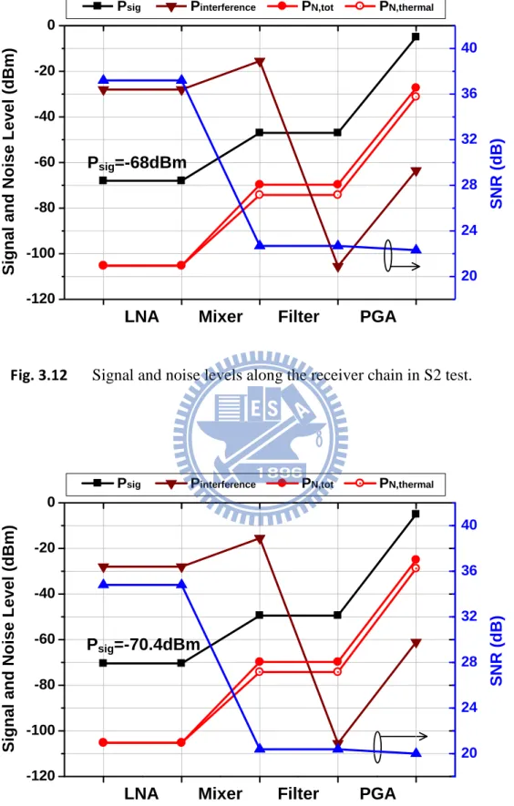
(15) List of Figures. List of Figures Fig. 2.1. Deterioration mechanisms due to: (a) harmonics and (b) image mixing .... 8. Fig. 2.2. Classical receiver architectures for DVB-T: (a) superheterodyne; (b) updown dual conversion; (c) single down-conversion low-IF........................ 9. Fig. 2.3. Block diagram of dierect conversion receiver with: (a) dedicated LNAs for each band, and (b) a broadband LNA.................................................. 11. Fig. 2.4. Block diagram of a DVB-T/H system ....................................................... 12. Fig. 2.5. Noise model for calculating C/N performance .......................................... 14. Fig. 2.6. Impact of phase noise on reciprocal mixing .............................................. 17. Fig. 2.7. Design trade-offs between the ABB filtering and ADC SNR.................... 19. Fig. 2.8. Impact of second-order intermodulation distortion ................................... 21. Fig. 2.9. Impact of third-order intermodulation distortion....................................... 22. Fig. 2.10. Impact of quadrature imbalance in a direct-conversion receiver .............. 23. Fig. 3.1. RF front-end gain settings versus input power levels................................ 27. Fig. 3.2. LO/RF leakage and generation of DC offsets............................................ 30. Fig. 3.3. Servo loop for DC offset cancellations ...................................................... 31. Fig. 3.4. NF versus gain settings in the analog baseband ........................................ 32. Fig. 3.5. Recommended LO/PLL phase noise mask ................................................ 34. Fig. 3.6. Noise contributions from different blocks in the maximum gain mode .... 36. Fig. 3.7. Pre-filtering effect at the mixer output ...................................................... 37. xiii.
(16) List of Figures. Fig. 3.8. IIP3 contributions from different blocks in the maximum gain mode ...... 38. Fig. 3.9. SNR versus RF Input power level in sensitivity test ................................. 40. Fig. 3.10 Signal and noise levels along the receiver chain in DR test ...................... 41 Fig. 3.11. SNR degradation along the receiver chain in DR test ............................... 41. Fig. 3.12 Signal and noise levels along the receiver chain in S2 test ....................... 45 Fig. 3.13 Margined signal and noise levels along the receiver chain in S2 test ....... 45 Fig. 3.14 Signal and noise levels along the receiver chain in L3 test ....................... 46 Fig. 3.15 Margined signal and noise levels along the receiver chain in L3 test ....... 46 Fig. 4.1. Illustration of substrate noise coupling from a digital back-end to an LNA ................................................................................................................... 50. Fig. 4.2. Capacitor Cross-Coupled CG-LNA configuration .................................... 52. Fig. 4.3. Noise-canceling Balun LNA configuration ............................................... 53. Fig. 4.4. LNA configured as either (a) differential input CCC-CG LNA, or (b) single-ended input Balun LNA ................................................................. 54. Fig. 4.5. Cascode current buffer (a) conventional CG buffer, (b) Gm-boosting technique with a feed-forward gain of +1 or -1, (c) the proposed CMR buffer ......................................................................................................... 55. Fig. 4.6. Simplified schematic for the analysis of M2 channel noise ...................... 57. Fig. 4.7. The proposed LNA configurations: (a) in the differential receiving mode; (b) in the single-ended receiving mode. .................................................... 59. Fig. 4.8. Simulated noise transfer gain and overall NF in (a) the proposed LNA, (b) the conventional Balun LNA .................................................................... 62. Fig. 4.9. The conventional LNA configurations: (a) in the differential receiving mode; (b) in the single-ended receiving mode. ......................................... 63 xiv.
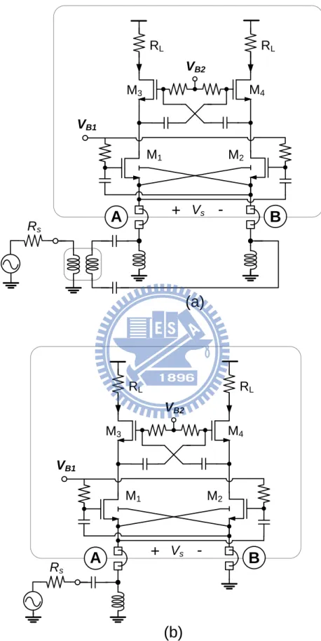
(17) List of Figures. Fig. 4.10. Die micrograph of the fabricated LNA...................................................... 64. Fig. 4.11. The measured S-parameters in the differential and signle-ended configurations............................................................................................ 65. Fig. 4.12 The measured NF of the proposed LNA and of the conventional LNA in (a) the single-ended (SE) configuration, and (b) the differential (DE) configuration ............................................................................................. 66 Fig. 4.13 The measured IIP2 and IIP3 of the proposed LNA and of the conventional LNA in (a) the single-ended (SE) configuration, and (b) the differential (DE) configuration .................................................................................... 67 Fig. 4.14 Simplified equivalent circuit for the analysis of the proposed CMR buffer ................................................................................................................... 71 Fig. 4.15 The equivalent circuit for the analysis of the CG-CS amplifier in cascode with the CMR buffer, including the noise sources from each device ....... 71 Fig. 4.16 Contour plots of normalized (a) io1 and (b) io2 as the functions of ro1 and ro2. ............................................................................................................. 73 Fig. 4.17 Contour plot of differential output mismatch by sweeping ro1 and ro2 with input mismatch of ε=0.2 and θ=20°: (a) amplitude mismatch, and (b) phase mismatch. ........................................................................................ 73 Fig. 4.18. AI1/AI2 and transfer gains of M1—M4 channel noise and Rs noise currents by sweeping gm1 for two cases with the CMR or the conventional CG buffer. ........................................................................................................ 76. Fig. 4.19. The calculated NF, voltage gain, and S11 versus gm1.................................. 76. Fig. 4.20. The equivalent circuit for the analysis of the M1/M2 distortion currents.. 78. Fig. 4.21. The transfer gains of harmonic distortion currents with the CMR buffer or xv.
(18) List of Figures. the conventional CG buffer. ...................................................................... 79 Fig. 4.22 Simplified schematic for the analysis of bandwidth limitation.. ............... 80 Fig. 4.23 Simplified schematic for exploring noise-canceling mechanism at high frequencies.. .............................................................................................. 82 Fig. 4.24 Magnitude response of M1 noise current.. ................................................ 83 Fig. 4.25. Phase response of M1 noise current ......................................................... 84. Fig. 4.26 Measured amplitude imbalance: a) the proposed LNA, and b) the LNA using the conventional CG buffer.. ........................................................... 86 Fig. 4.27 Measured phase imbalance: a) the proposed LNA, and b) the LNA using the conventional CG buffer. ...................................................................... 86 Fig. 4.28 Caculated NF versus gm1 with different ratio k.. ........................................ 88 Fig. 4.29. Die micrograph of the fabricated LNA...................................................... 89. Fig. 4.30 Measured NF versus frequency with different ratio k... ............................ 89 Fig. 5.1. Block diagram of the designed RF tuner ................................................... 92. Fig. 5.2. Simplified schematic of RF front-end at UHF band.................................. 94. Fig. 5.3. The designed RFVGA topology ................................................................ 95. Fig. 5.4. Front-end configuration: (a) at high-gain mode, and (b) at low-gain mode ................................................................................................................... 98. Fig. 5.5. Simplified schematic for noise analysis of the TIA................................. 100. Fig. 5.6. Architecture of the divide-by-four divider, and the designed D-latch circuits ..................................................................................................... 101. Fig. 5.7. Simplified diagram of successive-detection logarithmic amplifiers ....... 102. Fig. 5.8. Architecture of Analog Baseband ............................................................ 103. Fig. 5.9. (a) Architecture of the RC calibration loop. (b) Timing diagram of the RC xvi.
(19) List of Figures. calibration loop ....................................................................................... 105 Fig. 5.10 Schematic of VCOs ................................................................................. 107 Fig. 5.11. Programmable bias current (3-bit is shown) ............................................ 110. Fig. 5.12. Equivalent circuit of interconnection between the pad and the lead ....... 111. Fig. 5.13 Schematic of a bidirectional LO testing buffer........................................ 112 Fig. 5.14. Die photograph ........................................................................................ 113. Fig. 5.15 Measured overall NF versus the RFE and ABB gain settings ................. 114 Fig. 5.16 Measured NF at different IF frequencies ................................................. 115 Fig. 5.17 Phase noise profile measured at synthesizer output ................................ 116 Fig. 5.18 Measured locking process of frequency synthesizer ............................... 116 Fig. 5.19 Measured C/(N+I) vs. input power for the test chip comprising digital front-end. ................................................................................................. 117 Fig. 6.1. Simplified schematic of the designed LNAs ........................................... 122. Fig. 6.2. Simulated S11 of the designed LNAs ...................................................... 124. Fig. 6.3. Simulated NF of the designed LNAs ....................................................... 125. Fig. 6.4. Simulated voltage gain of the designed LNAs ........................................ 125. Fig. 6.5. The die micrograph of the chip................................................................ 126. Fig. 6.6. Simplified block diagram of testing chip ................................................ 128. Fig. 6.7. Flowchart of chip verification ................................................................. 128. Fig. 6.8. The photograph of the actual PCB for COB test ..................................... 129. Fig. 6.9. Bonding diagram in a 40-pin QFN package ............................................ 129. Fig. 6.10. The photograph of the actual PCB for package test ................................ 130. Fig. 6.11. Output SNR in a single-ended mode as the digital part is on/off ............ 132. Fig. 6.12. Output SNR in a differential mode as the digital part is on/off ............... 132 xvii.
(20) List of Figures. Fig. 6.13 A star configuration of VDD pins ............................................................ 133 Fig. 6.14 Clock leakage to the RF input with shared power/ground planes ........... 135 Fig. 6.15 Clock leakage to the RF input with separate power/ground planes ........ 135 Fig. 6.16 Measurement setup with an external LDO .............................................. 139 Fig. 6.17 Photograph of actual PCB in the differential receiving mode ................. 139 Fig. 6.18 Measured input return loss in both two receiving modes ........................ 140 Fig. 6.19 Measured gain flatness across the band (RFE=max, ABB=50dB) .......... 140 Fig. 6.20 Measured NF in the high-gain mode (RFE=max, ABB=50dB) .............. 141 Fig. 6.21 Measured NF in the low-gain mode (RFE=max, ABB=50dB) ............... 141 Fig. 6.22 Measured IIP3 and IIP2 in the high-gain mode (RFE=max, ABB=50dB) ................................................................................................................. 142 Fig. 6.23 Measured spectrum at the baseband output with the RF port terminated to a 50ohm terminator; clock leakage component at 2MHz is measured at the gain setting of 93dB .......................................................................... 142 Fig. 6.24 Signal quality deterioration due to the clock leakage, measured with the RF port having an input of -96.6dBm QPSK signal ............................... 143 Fig. 6.25 Measured clock leakage level referred to the RF input across the band of interest ..................................................................................................... 143 Fig. 6.26 Measured phase noise spectrum at the VCO output (2.844GHz) ............ 144 Fig. 6.27 Measured phase noise spectrum at the baseband output at the 474MHz channel (LO=2.844GHz/6) ..................................................................... 144 Fig. 6.28 Measured constellation diagram of DVB-H signal (64-QAM 3/4) ......... 145 Fig. 6.29 Measured MER (EVM) per subcarrier for DVB-H signal (8k mode) ..... 145 Fig. 6.30 Measured performance overview for DVB-H signal (8k mode) ............. 146 xviii.
(21) List of Figures. Fig. 6.31 Measured MER versus the input power level (64-QAM 3/4) ................. 146 Fig. 6.32 Measured MER versus the input power level (QPSK 1/2) ...................... 147 Fig. 6.33 Simplified schematic of the UHF front-end with an auxiliary LNA ....... 152 Fig. 6.34. The die micrograph of the high sensitivity tuner chip ............................. 153. xix.
(22) List of Figures. xx.
(23) Abbreviations. Abbreviations 4G ABB ADC AFC AGC ATT AWGN BBP BCC BER BOM BW C/N CCC CD CG CML CMMB CMOS CMR CMRR COB CR CS CW dB dBv DC DCC DCOC DR DSB. 4th Generation Analog Baseband Analog-to-Digital Converter Adaptive Frequency Calibration Automatic Gain Control Attenuation Additive White Gaussian Noise Baseband Processor Bulk Cross-Coupling Bit Error Rate Bills of Material Bandwidth Carrier-to-Noise Capacitor Cross-Coupling Common Drain Common Gate Current-Mode Logic China Mobile Multimedia Broadcasting Complementary Metal-Oxide Semiconductor Common-Mode Rejecting Common-Mode Rejection Ratio Chip on a Board Coding Rate Common Source Continuous Wave Decibel Decibel Volt (peak) Direct Current Dual Cross-Coupling DC Offset Cancellation Dynamic Range Double Side Band xxi.
(24) Abbreviations. DSP DVB-H DVB-T ESD ETSI EVM F ft GSM I/Q I2C IF IIP2 IIP3 IM2 IM3 IMD IMRR ISDB-T k LDO LG LNA LO LPF LTE MBRAI MediaFLO MER MIM MMIC NF NMOS OFDM PAL PAPR PCB PGA PLL PMOS. Digital Signal Processing Digital Video Broadcasting–Handheld Digital Video Broadcasting–Terrestrial Electrostatic Discharge European Telecommunications Standards Institute Error Vector Magnitude Noise Factor Transit frequency Global System for Mobile communications In-phase/quadrature Inter-Integrated Circuit Intermediate Frequency 2nd-order Input Referred Intercept Point 3rd-order Input Referred Intercept Point 2nd-order Intermodulation 3rd-order Intermodulation Intermodulation Distortion Image Rejection Ratio Integrated Services Digital Broadcasting – Terrestrial Boltzmann constant Low-Dropout Regulator Low-Gain Low Noise Amplifier Local Oscillator Low Pass Filter Long Time Evolution Mobile and portable DVB-T/H Radio Access Interface Media Forward Link Only Modulation Error Ratio Metal-Insulator-Metal Capacitor Monolithic Microwave Integrated Circuit Noise Figure N-Channel Metal-Oxide Semiconductor Orthogonal Frequency-Division Multiplexing Phase Alternate Line Peak to Average Power Ratio Printed Circuit Board Programmable Gain Amplifier Phase-Locked Loop P-Channel Metal-Oxide Semiconductor xxii.
(25) Abbreviations. PVT QAM QFN QPSK RF RFC RFE RFIC RSSI Rx SAW SMA SNIR SNR SoC T T-DMB TIA U/D UHF VCO VDD VGA VGCF VGLNA VHF VSA WiMAX WLAN. Process, Voltage, Temperature Quadrature Amplitude Modulation Quad Flat Non-leaded package Quadrature Phase Shift Keying Radio Frequency RF Chock RF Front-End Radio Frequency Integrated Circuit Received Signal Strength Indicator Receiver Surface Acoustic Wave SubMiniature version A Signal-to-Noise- and-Interference Ratio Signal-to-Noise Ratio System-on-a-Chip Absolute temperature Terrestrial Digital Multimedia Broadcasting Transimpedance Amplifier Unwanted-to-Desired power ratio Ultra-High Frequency Voltage Control Oscillator Power Supply Voltage Variable Gain Amplifier Variable-Gain low-pass Channel Filter Variable-Gain LNA Very High Frequency Vector Signal Analyzer Worldwide Interoperability for Microwave Access Wireless Local Area Network. xxiii.
(26) Abbreviations. xxiv.
(27) Chapter 1 Introduction 1.1 Background In recent years, television broadcasting systems all over the world have been gradually switching over from analog to digital. These digital broadcasting technologies bring several advantages in bandwidth efficiency, robustness, and signal quality. Currently, technological developments have introduced mobile TV, making it possible to efficiently receive TV channels and other high bit-rate services in handheld devices. In order to support these new applications, the existing broadcast TV standards are augmented to meet the more demanding requirements on mobile receptions. This chapter provides an overview of mobile TV standards.. 1.2 Overview of Mobile TV Standards There exist several mobile TV standards being developed and emerging around the world. Each of them dominates the mobile TV technology in different parts of the world and till date there is no single globally accepted standard. Below listed are main dominant mobile TV standards along with their brief profiles. Digital Video Broadcasting–Handheld (DVB-H) [1] is a standard proposed by the DVB Group for the delivery of digital multimedia content to mobile, handheld devices. The physical layer of DVB-H systems essentially conforms to the DVB-T specification, with a limited number of extensions. The new features make it possible 1.
(28) Chapter 1. Introduction. to efficiently receive high data-rate services in battery-powered devices. To increase power saving, each service is transmitted in bursts with a typical 1:10 on/off ratio using the whole available bandwidth. As claimed in the DVB-H standard, this time slicing technique can reduce the power consumption up 90 percent with respect to a non-time-sliced. transmission.. On. the. other. hand,. the. Multi-Protocol. Encapsulation–Forward Error Correction (MPE-FEC) technique is introduced to increase the carrier-to-noise (C/N) and Doppler performance in mobile channels. The DVB-H system is fully compatible with the DVB-T network and system, allowing for the use of the existing DVB-T equipments. It utilizes a part of the frequency range for DVB-T, including VHF III and UHF bands with a channel bandwidth of 6/7/8MHz. In addition, a 5MHz channel in L-band (1670-1675MHz) has been allocated for the DVB-H operation in the United States. In Europe, the additional usage of 1450-1490MHz L-band is also discussed. Terrestrial Digital Multimedia Broadcasting (T-DMB) [2] was developed in South Korea, and its physical parameters are identical to the European DAB (Digital Audio Broadcasting) standard. T-DMB uses OFDM technology and operates with a 1.536MHz bandwidth. For the mobile reception, its frequency band is allocated at VHF III and 1450-1492MHz bands. It offers 1.06 Mbits/s – 2.3 Mbits/s data rate. Integrated Services Digital Broadcasting – Terrestrial (ISDB-T) [3] was developed in Japan since 1999, and also adopted as Brazil’s standard in 2006. ISDB-T uses a COFDM multicarrier system as in DVB-T, but is more complex and robust. The 6 MHz-wide channel can be subdivided into 13 segments. One segment has a width of 430 kHz with a guard band of about 200 kHz each for the upper and lower adjacent channels. The allocated spectrum is VHF and L-band. MediaFLO (Media Forward Link Only) [4] was developed by Qualcomm to effectively address key challenges involved in the wireless delivery of multimedia content to mass consumers. It utilizes OFDM modulation schemes and supports frequency bandwidths of 5/6/7/8 MHz. In a 6 MHz channel, the FLO physical layer can achieve up to 11.2 Mbps at this bandwidth. In USA, the FCC assigned licenses for 698-746 MHz in 6 MHz blocks for advanced mobile services. China Mobile Multimedia Broadcasting (CMMB) [5] is a mobile TV and multimedia standard developed and specified in China since 2006. The CMMB system is a mixed satellite and terrestrial wireless broadcasting system, which utilizes 2.
(29) Chapter 1. Introduction. two S-band satellites to cover the digital video broadcasting (DVB) over a wide area, while the cellular base stations in the populated metropolitan areas. The service operates in both S-band (2635-2660MHz) and U-band (470-860MHz). The channel bandwidth can be either 2 or 8 MHz, depending on the data rate. Summarized in Table 1.1, these standards have some common characteristics such as OFDM modulation and frequency allocations among VHF III, UHF, and L-band. The global fragmentation of mobile TV standards will ultimately lead to strong demands for multi-standard mobile TV solutions. It is also a fact that two or more standards begin to coexist within one country. In general, mobile TV subsystems are divided into two main parts: RF tuner and digital demodulator. The tuner receives the desired TV channel and converts it to the baseband for further signal processing in the demodulator. The demodulated signal is then decoded and displayed on the LCD panel. To achieve high-performance high-quality signal receiving, the tuner is a critical part. This dissertation attempts to address the tuner design for such mobile devices in advanced CMOS technologies. Although this research mainly targets for the DVB-H standard that appears to be the most popular in more countries, many design aspects could be generalized to most other standards.. Table 1.1 Overview of several mobile TV standards Standard Area RF Spectrum (MHz). Channel Bandwidth Modulation Data rate (Mbps) Required C/N. DVB-T/H EU 470-862 174-240 1670-1675 1452-1492. T-DMB Korea 174-240 1452-1492. ISDB-T Japan 470-770 90-222 -. MediaFLO USA 696-746 2605-2655 -. CMMB China 470-798 2635-2660 -. 5/6/7/8. 1.536. 0.43-1.29. 6. 8. COFDM 4-64 QAM 4.98-21.11. COFDM DQPSK 1.06-2.3. COFDM 4-16 QAM 2.8-11.2. COFDM -16.24. ~25. ~7. COFDM 4-16 QAM 0.28-1.79 (per seg.) ~12. ~12. ~25. 3.
(30) Chapter 1. Introduction. 1.3 Dissertation Organization Chapter 2 discusses how to obtain RF specifications from the system specifications. Based on the DVB-T/H standard, RF specifications such as voltage gain, noise figure (NF), input third-order intercept point (IIP3), and phase noise can be calculated from the system standard that specifies sensitivity, selectivity, and linearity test patterns. Chapter 3 deals with distributing the building block specifications from the derived RF specifications. Based on analytical expressions, spread-sheet tables are constructed to distribute the requirements among the receiver blocks. Link budget analysis and system design verification are also discussed for a complete design procedure. Chapter 4 presents a single-stage wideband low-noise amplifier (LNA) with a differential output, but a reconfigurable single-ended or differential input. The proposed common-mode rejecting (CMR) buffer significantly improves noise figure (NF) and linearity, making it possible to support a dual-mode operation. The LNA realized in 0.13μm CMOS technology achieves 23dB voltage gain, 0dBm IIP3, and 2.5dB NF in either differential or single-ended receiving mode, while consuming only 3mW. Chapter 5 presents a fully integrated dual-band DVB-H tuner implemented in 0.13μm CMOS technology. The subsystem design includes the RF front-end, the analog baseband, and the frequency synthesizer. Considerations on RF integration design are also illustrated. With a single-ended input configuration, the tuner achieves a sensitivity level of -96.6dBm and dissipates 114mW from a 1.2 V supply. Chapter 6 illustrates design considerations as the technology scales from 0.13μm to 65nm. The LNA is used as an example to evaluate the performance at the sub-GHz band in 65nm design compared to 0.13μm case. Two integrated receiver prototypes were realized in 65nm CMOS. The first receiver was implemented to demonstrate even higher levels of noise immunity. The proposed LNA compatible for differential and single-ended inputs was integrated for system-level evaluations. The second receiver was implemented to demonstrate even better sensitivity performance with an asymmetric LNA, achieving an NF less than 3.5dB across the band of interest. The performance verification of the tuner is described in detail. 4.
(31) Chapter 1. Introduction. Chapter 7 concludes this dissertation and discusses the future research directions for mobile TV technologies.. 5.
(32) Chapter 1. Introduction. 6.
(33) Chapter 2 Receiver Architectures and Specifications The specifications for the DVB-T/H tuner are contained in the mobile and portable DVB-T/H radio access interface (MBRAI) document [6], [7]. MBRAI details radio specifications in terms of modulation formats, bit error rates (BER), carrier-to-noise (C/N) requirements, sensitivity, and selectivity/ linearity patterns. Although these parameters are commonly seen in wireless standards, it is not straightforward to be used for RF/analog design. In this chapter, we will describe how to translate these system specifications into the RF specifications such as noise figure (NF), third-order intercept point (IP3), second-order intercept point (IP2), and phase noise [8].. 2.1. Receiver Architecture. 2.1.1 Classical Receiver Architectures Traditional analog and digital TV tuners have a wide bandwidth from 48 to 864MHz, imposing stringent requirements on the tuner performance characteristics such as harmonics and image rejections [9]. Fig. 2.1(a) and (b) illustrate the problems of harmonics and image mixing. Due to the wide bandwidth spanning several octaves, 7.
(34) Chapter 2. Receiver Architectures and Specifications. unwanted signals located around the harmonics of LO must be supressed to avoid down-conversion into the band of interest, otherwise it would deteriorate signal quality. Similarly, the unwanted image signal which is twice the IF away from the desired channel must be attenuated sufficiently to mitigate SNR degradation.. 48-862MHz. Desired signal Blockers. 0 fIF. fLO. 2fLO. 4fLO. 3fLO. 5fLO. (a). 48-862MHz. Desired signal Image. 0. fIF. (fLO-fIF). fLO. (fLO+fIF) (b). Fig. 2.1. Deterioration mechanisms due to: (a) harmonics and (b) image mixing.. In order to solve these problems, several different techniques have been proposed [10]-[14]. Conventional superheterodyne tuners are classical architectures, shown in Fig. 2.2 (a), which utilizes a bulky tunable tracking filter to filter out the higher band channels as well as the image channel. However, this architecture is not easy to implent monolithically because the RF tracking filter must have a high-Q factor and need external high control voltages to tune its selection frequency.. 8.
(35) Chapter 2. Receiver Architectures and Specifications. SAW 36/44 MHz. LNA. 48-862MHz. LO1 (a). SAW2. SAW1. 36/44 MHz. LNA. ~1.2GHz LO1. LO2. Low-IF. (b). IF PPF. RF PPF. Low-IF. LNA. 48-862MHz. RF BPF. LO (c). Fig. 2.2. Classical receiver architectures for DVB-T: (a) superheterodyne; (b) up-down dual conversion; (c) single down-conversion low-IF.. To eliminate the tunable high-Q tracking filter, an up/down dual-conversion architecture as shown in Fig. 2.2 (b) was proposed [11], [12]. A higher first intermediate frequency (IF) around 1.2GHz is chose to alleviate the problem of harmonics/image mixing by pulling the harmonics of the LO and image channels out of the TV band. However, an external surface acoustic wave (SAW) filter is still needed to select the desired channel at the fixed first IF. Prior to the second down-conversion to a lower second IF at 36/44MHz for standard TV demodulation, 9.
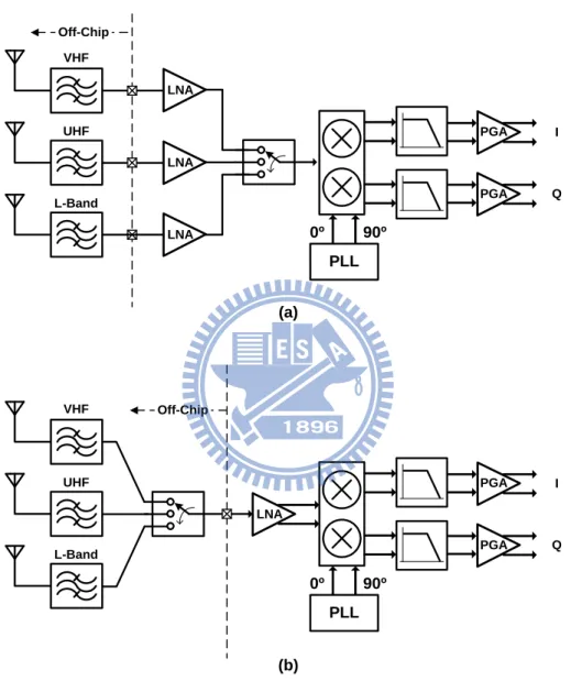
(36) Chapter 2. Receiver Architectures and Specifications. the first-IF SAW filter msut provide an image rejection of 30-40dB. To achieve a required image rejection up to 60dB totally in system considerations, therefore, the remaining 30dB of image rejection can be done by using an image rejection mixer (IRM) in the second down-conversion. The drawback of this architecture is the need for an external SAW filter, which limits the level of integration and raises the power dissipation. Compared with the dual-conversion architectures, [13], [14] employs a single down-conversion low-IF architecture to increase the level of integration, shown in Fig. 2-2 (c). This topology relaxes the requirements of RF filters. Unwanted signals at and above 5 times the wanted signal frequency should be supressed; as a result, RF filters can be integrated on chip. In addition, a double quadrature mixer [15] is implemented to obtain an image suppression better than 60dB at the cost of higher system complexity.. 2.1.2 Direct-Conversion Receiver Architectures As mentioned earlier, classical TV tuners consume much power of 0.5-1W to overcome the technical bottlenecks and generally need external tracking and SAW filters which are expensive and bulky for channel selection as well as image rejection. Obviously, such solutions are not appropriate in mobile TV applications. In the battery-powered handheld devices, the constraints of low power consumption and small form factor demand a simplified tuner architecture that differ from classical architectures. Since only a part of classical TV broadcast band (48-864MHz) has been allocated to mobile TV spectrum, the problem of hamonics and image mixings is much relaxed. More specifically, most mobile TV standards target on the use of VHF III (174-230MHz), UHF- (470-862MHz), and L-bands (1452-1492MHz and 1670-1675MHz). For battery-powered handheld devices, thus, a direct conversion receiver (DCR) architecture seems to be a promising architecture in realizing a low cost, small form factor, low power consumption highly integrated DVB-T/H receiver.. As shown in Fig. 2.3, two configurations can be selected to implement the tuner architecture. In [16]–[18], state-of-the-art solutions generally utilize dedicated LNA or front-end circuits for each band as shown in Fig. 2.3 (a), where seperate LNAs is 10.
(37) Chapter 2. Receiver Architectures and Specifications. shown as the example. Such solutions eliminate the need for an external switch and facilitates the connections to seperate RF band-selection filters. Most of all, seperate RF circuits can be optimized for each band with reduced power consumption.. Off-Chip VHF LNA UHF. PGA. I. PGA. Q. PGA. I. PGA. Q. LNA L-Band. 0º. LNA. 90º PLL. (a). VHF. Off-Chip. UHF LNA L-Band. 0º. 90º PLL. (b). Fig. 2.3. Block diagram of dierect conversion receiver with: (a) dedicated LNAs for each band, and (b) a broadband LNA.. Another technique is utilizing wideband techniques to cover multi-band operations as shown in Fig. 2.3 (b). This architecture requires a wideband front-end to support full band of mobile-TV services from 170 to 1700 MHz [19]. Wideband 11.
(38) Chapter 2. Receiver Architectures and Specifications. reception can minimize the hardware requirement on front-ends, but an external RF switch is needed to enable band selection in conjunction with seperate RF filters and antennas. Requirements on such external components typically limit the use of this architecture in manufactures, especially the need for external wideband balun if differential LNAs are adopted.. 2.2. RF Specifications Fig. 2.4 depicts the block partition of a DVB-T/H system. The defined. requirements are referred to the RF reference point at the input of the tuner. All the RF specifications in this thesis are derived based on an 8MHz channel bandwidth for the portable or hand-held convergence terminals (terminal category b2 or c), unless otherwise stated.. Optional RF Tuner. Reference Point. Fig. 2.4. DVB-T/H Demod. TS. Required C/N. Block diagram of a DVB-T/H system.. 2.2.1 Frequencies and Channel Bandwidths The European Telecommunications Standards Institute (ETSI) initially allocates the frequency bands covering UHF IV and V for the terminal category b2 or c. The receiver should be able to support 6/7/8MHz channel bandwidths, depending on the region. Table 2.1 illustrates the centre frequencies for various channel bandwidths, in which flexible offset frequencies of n 1 6 MHz and n {1, 2, ...} should be 12.
(39) Chapter 2. Receiver Architectures and Specifications. guaranteed. The frequency range is 470-862MHz for category b2, while limited to 754MHz in a TV-GSM co-integrated terminal (category c). Since GSM uplink at 880MHz is close to the TV spectrum, a GSM rejection filter is needed at the receiver input to avoid nonlinear distortions and reciprocal mixing issues due to strong GSM interferers. Together with the coupling losses between antennas (~10dB) [20], the filter must provide high attenuation (~50dB) to suppress the GSM transmitted power from +33dBm to -28dBm, which is the maximum allowed signal level at the receiver input for DVB-H. Under the case with a GSM rejection filter, the overall noise figure can be up to 6 dB [6].. Table 2.1 Channel bandwidth and centre frequencies in MBRAI Channel BW [MHz] 8. System Noise BW [MHz] 7.61. 7. 6.65. 6. 5.71. Channel Centre Frequencies [MHz] 474 N 21 8 f offset , N 21,,69 474 N 21 8 f offset , N 14,,83. 473 N 14 6 f offset , N 14,,83. 2.2.2 C/N Requirement In MBRAI, the C/N performance is calculated based on the noise model as illustrated in Fig. 2.5. Assume that the incoming signal is amplified and down-converted by a front-end stage which has an overall noise factor FRX and perfect automatic gain control (AGC). The relative excess noise Px denotes several impairments such as phase noise, quantization noise, etc. For giving the reference BER (2×10⁻⁴), the carrier-to-noise ratio (C/N ratio) at the demodulator input can be derived for a particular modulation scheme. The main C/N requirements for different modulation schemes are listed in Table 2.2.. 13.
(40) Chapter 2. Receiver Architectures and Specifications. Tuner with ideal AGC Practical but unimpaired demodulator. Excess 'backstop' noise Px (relative to C) Noise figure F. Fig. 2.5. Gain G=1/C. Noise model for calculating C/N performance.. Table 2.2 C/N requirements versus modulation schemes Modulation Scheme QPSK 1/2 code rate. C/N Requirement in Gaussian Channel 4.6. C/N Requirement in Portable outdoor channel 10.5. 16-QAM 2/3 code rate. 12.7. 19.5. 64-QAM 3/4 code rate. 19.9. 27.5. 2.2.3 Minimum Input Levels The receiver sensitivity, defined as the minimum signal input level that a receiver can detect and maintain a target BER, is given by S min dBm 10 log10 kT 10 log10 BW NFRX . C N. (2.1). where k=1.38×10⁻²³ J/°K is Boltzmann constant, T=290∘K is ambient temperature, BW is signal bandwidth, NFRX is overall receiver noise figure, and C/N is the minimum required signal-to-noise ratio. Since MBRAI 2.0 requires a NF below 4dB at the sensitivity level, the sensitivity target for 8MHz channel bandwidth shall be lower than -96.6dBm for QPSK 1/2 modulation scheme, where 7.61 MHz of effective bandwidth and 4.6dB of SNR requirement are specified.. 14.
(41) Chapter 2. Receiver Architectures and Specifications. 2.2.4 Dynamic Gain Range In the absence of any interference, the maximum desired signal level at the tuner input is specified to be -28dBm. Since the minimum sensitivity level is -96.6dBm, the tuner has to provide at least 68.6dB gain range. Assume that the maximum rail-to-rail voltage swing at the tuner output from a supply of 1.2V is 2Vp-p differentially, i.e., 10dBm referred to 50Ω resistance. As a peak-to-average power ratio (PAPR) of 15dB is taken into account, a reasonable power level at the tuner output would be maintained at -5dBm for all input power levels and gain settings. As a result, the tuner should provide a gain range from 22.6 to 91.6dB at least.. 2.2.5 Interference Test Patterns The wide frequency spectrum of DVB-T/H causes the issue that the desired signal usually comes with multiple in-band interferers. This issue becomes important when the desired signal is weak and adjacent-channel interferers are strong at the receiver input. Several types of interference tests are specified in the MBRAI document to characterize reception conditions in the presence of other interfering TV channels. They can be divided into two categories: 1) receiver selectivity testing with a single analog or digital interferer, and 2) receiver linearity testing with two analog and/or digital TV interferers. Table 2.3 and Table 2.4 respectively illustrate these test patterns, where D represents desired channel signal power and U is unwanted interferer signal power.. Table 2.3 Selectivity test patterns Selectivity Pattern. Modulation of interferer. S1. analog. S2. digital. Interferer location N±1. U/D Ratio [dBc] 38. U [dBm]. N±k (k>1). 48. -28. N±1. 29. -35. N±k (k>1). 40. -28. 15. -35.
(42) Chapter 2. Receiver Architectures and Specifications. Table 2.4 Linearity test patterns Linearity Pattern. Modulation of interferer Digital and analog. Interferer location N+2 (digital). U/D Ratio [dBc] 40. L1. U [dBm]. N+4 (analog). 45. L2. analog. N+2, N+4. 45. -35. L3. digital. N+2, N+4. 40. -35. -35. The selectivity patterns measure a receiver's ability to receive a desired signal in the presence of an unwanted interferer at an adjacent/alternate channel close to or away from the desired channel. In general, this test item is mainly concerned with three performance parameters: 1) the attenuation ratio of the channel selection filter to the adjacent/alternate interferers, 2) the phase noise and spurs of the synthesized LOs. The linearity patterns are mainly utilized to evaluate the corruption of the desired signal due to the third-order intermodulation (IM3) of two nearby interferers. If a weak desired signal along with two strong interferers enter a nonlinear circuit and experience the third-order nonlinearity in that circuit, then one of the IM3 might fall in the band of interest and corrupts the desired signal. Third-order distortion is specified in terms of an input referred third-order intercept point IIP3.. 2.2.6 Phase Noise and LO Spurs Ideally the synthesizer’s output spectrum should be a Dirac impulse at the desired frequency. But practical signal sources usually have sidelobes in the frequency spectrum due to the disturbance of several kinds of noise sources. To this nonideal effect, there are two main mechanisms that create distortion and noise components on the desired channel. First, the close-in phase noise of the LO causes the loss of orthogonality on the subcarriers due to the inter-subcarrier interference [21]. This mechanism degrades the modulation accuracy of desired signal, i.e., EVM, and is reflected in the requirement of integrated phase noise within the signal bandwidth or maximum tolerable rms 16.
(43) Chapter 2. Receiver Architectures and Specifications. phase error. To minimize this influence, MBRAI specifies the excess noise to be 33 dB lower than the LO signal level. In fact, 37dB at least should be guaranteed to allow for the presence of other impairments such as quadrature mismatch. Second, the reciprocal mixing of the LO phase noise with the adjacent/alternate channel interferers may also result in in-band interference [22]. This mechanism is depicted in Fig. 2.6. In order not to deteriorate the signal quality much, the phase noise requirements at different offset frequencies from carrier can be determined by. U C Lf 10 log BW 10 log(%) D N . (2.2). where U/D represents unwanted/desired power ratio in test scenario, C/N is the minimum required signal-to-noise ratio, BW is signal bandwidth, and the last term (%) denotes the contribution ratio to the overall impairments.. fLO. Analog TV carrier. Desired Channel. U/D. N. Fig. 2.6. After mixing. Desired Channel. N+1. Unwanted Signal (Reciprocal mixing). 0. Impact of phase noise on reciprocal mixing.. According to S1 pattern in MBRAI2.0, analog TV (PAL/SECAM) interference at N+1 adjacent channel is up to 35 dB stronger than the wanted 64-QAM signal. From PAL signal definitions, its signal power is concentrated at the picture carrier, which is 1.25 MHz away from the boundary as shown in Fig. 2.6. This implies that the picture carrier is only 5.25 MHz away from the center of the wanted channel. For this demodulation, the minimum required SNR is 20dB and the signal bandwidth is 7.61MHz. Thus, the integrated phase noise from 1.45 to 9.05 MHz offset from the LO 17.
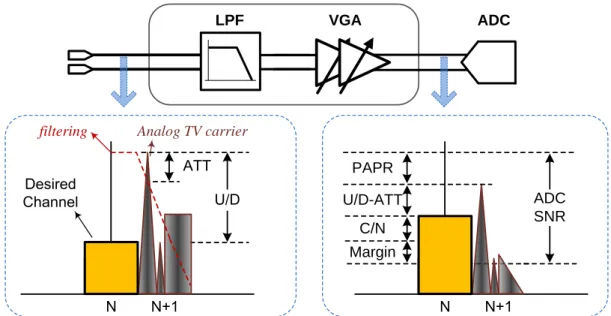
(44) Chapter 2. Receiver Architectures and Specifications. can be calculated.. . LO 9.05MHz. LO 1.45MHz. . LO 9.05MHz. LO 1.45MHz. U C Lf 10 log(%) D N . (2.3). Lf 35 20 5 60dBc. (2.4). The calculation shows that integrated phase noise from 1.45 to 9.05MHz offset should be less than –60dBc with a 5dB margin. Assume a rectangular phase-noise distribution within the channel. This translates to a phase-noise requirement of -129dBc/Hz at 1.45MHz away from the center. Actually, this assumption overestimates the requirement at 1.45MHz, which ensures that the phase noise profile can meet all the requirements with sufficient margins. With respect to the (N+2) adjacent interferer, two channels away from the desired signal in S1 pattern, analog TV interference may be 43dB higher than the wanted 64-QAM signal. This requires that the integrated phase noise from 9.45 to 17.05 MHz offset from the LO should be less than –68dBc. Similarly, this translates to a phase-noise requirement of -137dBc/Hz at 9.45MHz offset from the LO. The influence of frequency spurs acts very similarly to phase noise. They reciprocal-mix the adjacent/alternate channel interferers down into signal bands and contribute distinct terms in integrated phase noise. To evaluate this impact, the integrated phase noise across the frequencies of interest should include the power of LO spurs within this bandwidth.. 2.2.7 Filter Response Another IC specification relative to the selectivity patterns is concerned with the rejection ratio of the channel selection filter to the adjacent/alternate interferers. Since the received signal contains not only the desired channel but some neighboring interference channels, baseband filters are needed to separate the desired channel from unwanted interference channels. In general, the filtering can be done either in the analog or digital domain. Theoretically it is preferable to realize as much filtering as possible in the digital domain because digital filters has high accuracy against process,. 18.
(45) Chapter 2. Receiver Architectures and Specifications. voltage, temperature (PVT) variations and do not require tuning circuitry. However, pushing more filtering into the digital domain increases the required dynamic range and resolution in the ADC. Unfortunately, this significantly increases power consumption since the power of Nyquist rate ADC is proportional 2N where N is number of bits [23]. From a power dissipation and area perspective, as a result, some combination of analog and digital filtering will be an optimal choice. There is a tradeoff among the filter’s out-of-band attenuation, the maximum VGA gain and the dynamic range of the ADC. The residual adjacent channel power after the analog channel-select filter increases the required dynamic range in the ADC. In order not to saturate the ADC, the maximum signal magnitude at the receiver output should not exceed the allowable full swing of the ADC. Fig. 2.7 shows the SNR and SNDR requirement of the ADC, which is constrained mainly by the required adjacent channel immunity.. SNR U D C N PAPR ATT Margin (in dB). (2.5). where U/D represents the unwanted-to-desired signal ratio, C/N is the minimum required carrier-to-noise ratio for a specific modulation scheme; PAPR is the peak-to-average power ratio of the unwanted OFDM signal; ATT represents the out-of-band attenuation of the filter.. LPF. filtering. VGA. ADC. Analog TV carrier ATT. Desired Channel. PAPR U/D. ADC SNR. U/D-ATT C/N Margin. N. Fig. 2.7. N+1. N. N+1. Design trade-offs between the ABB filtering and ADC SNR. 19.
(46) Chapter 2. Receiver Architectures and Specifications. According to S2 pattern in MBRAI 2.0, digital TV (DVB-T) interference at N+1 adjacent channel is up to 29 dB stronger than the wanted 64-QAM signal. To maintain a minimum 20dB C/N requirement, 15 dB PAPR, 14dB margin, the SNR requirement of the ADC is calculated as (79-ATT) in dB. In order to conform to most of commercial demodulator ICs which own different ADC specifications, the target SNDR of the ADC is expected to be as low as 48dB (~8bits). This implies that the analog filter must provide at least 30dB of attenuation at 5.25MHz offset from the center frequency. Here, 5.25MHz refers to the carrier frequency of analog TV interference at the adjacent channel (N+1).. 2.2.8 IIP2 requirement In a direct conversion receiver, two nearby interferers can directly mix with each other and produce the IM2 component (f1 – f2). It is important to note that digital interferers can create broadband baseband interference due to the interactions among sub-carriers of the OFDM blocker in frequency domain. The interfering product would fall in the band of interest and degrade the performance of the receiver as shown in Fig. 2.8. In order to maintain the minimum SNR requirement, such a product must be suppressed, which could be approximated by an IM2 analysis using two-tone power series expansions. Calculation of the in-band interference can be expressed as C PIMD 2 2 PN m 3 IIP2 Psig 10 log(%) N. (2.6). where PN+m represents the total power of the digital interferers which is m channels away from the desired channel. Since the interferer is approximated by two tones with the same power, half the total power each, i.e., 3dB lower, should be considered for calculations. Moreover, total noise and interference power PN+I should be distributed (%) since several different interfering products, such as IM3, phase noise, etc., are created simultaneously. Thus, the minimum IIP2 is given by. 20.
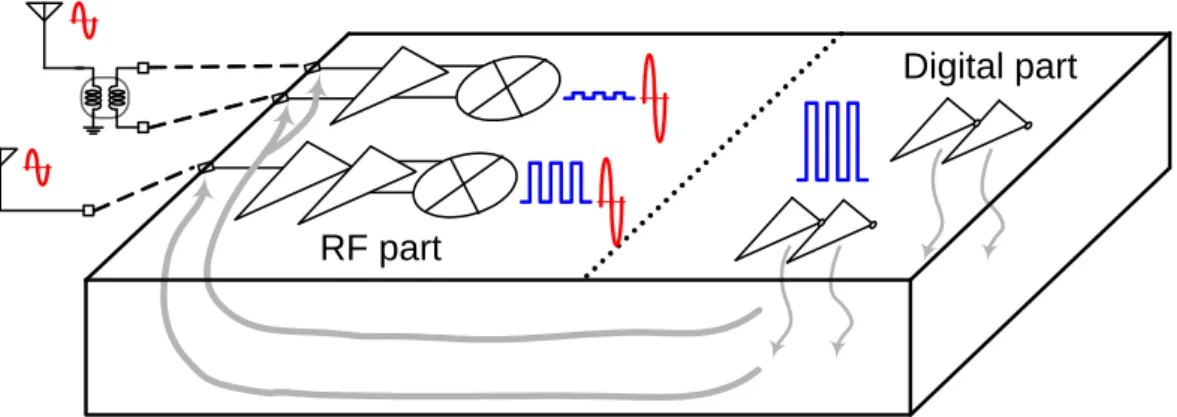
(47) Chapter 2. Receiver Architectures and Specifications. C IIP 2 2 PN m Psig 10 log(%) 6 N. (2.7). Since the standard defines the digital TV interference 2 channels away at –28 dBm and the wanted 64-QAM signal at –68 dBm, assuming 10% noise power contribution and 20 dB SNRmin, it can be easily found that the required IIP2 at the input is higher than +36 dBm under the S2 pattern test. Normally the IIP2 of a receiver is dominated by the mixer due to the high gain of the LNA and AC coupling between LNA output and mixer output. Thus, much attention on the input transconductance stage of the mixer for a symmetric design and layout should be paid to ensure a high IIP2.. DVB-T Interferer. fLO Desired Channel. 2nd order non-linearity. Desired Channel. U/D IMD2. N. Fig. 2.8. N+2. 0. Impact of second-order intermodulation distortion.. 2.2.9 IIP3 requirement As shown in Fig. 2.9, two unwanted interferers may create intermodulation products which fall in the desired channel due to the third-order nonlinearity of the receiver. To achieve enough SNR, the IM3 product should be limited, which can be approximated corresponding to the traditional formula based on two-tone analysis [8]. The required input referred IM3 product is derived as C PIMD 3 2 PN 2 PN 4 2 IIP3 Psig 10 log(%) N. (2.8). where PN+2 and PN+4 respectively represents interferer signal power at N+2 and N+4. 21.
(48) Chapter 2. Receiver Architectures and Specifications. channel. According to L3 test pattern, two digital TV interferers located at two and four channels away from the deisred channel will produce an IM3 product which falls into the desired channel. Since the power level of both two interferers is -35dBm with a requirement of unwanted-to-desired power ratio (U/D) higher than 40dB, the maximum allowable noise plus interference power level must be –87.7dBm to ensure a minimum SNR of 12.7dB for 16-QAM 2/3 modulation. Assume that the IMD3 interference contributes 50% of the total noise plus interference power, i.e., –87.7dBm–3dB =–90.7dBm. Hence, the IIP3 must be better than –7.15dBm. 1 U C IIP3 PN 2 10 log(%) 2 D N IIP3 35 . (2.9). 1 40 12.7 3 2. (2.10). Along with an IIP3 requirement of -7dBm, an NF less than 9.5dB is required to meet L1 and L2 tests simultaneously.. DVB-T Interferers. fLO. 3rd order non-linearity. Desired Channel. Desired Channel. U/D IMD3. N. Fig. 2.9. N+2. N+4. 0. Impact of third-order intermodulation distortion.. 2.2.10 Image Rejection In a direct-conversion receiver, the LO frequency is equal to the center frequency of the desired channel. Since the desired signal spectrum is spanned on both sides of the LO, the image of the desired channel is the desired channel itself. In order to maximize spectral efficiency, OFDM techniques are quickly becoming a popular 22.
(49) Chapter 2. Receiver Architectures and Specifications. method for advanced communications networks, including DVB-H. Since OFDM signals have asymmetrical spectrum, i.e., the upper sideband are uncorrelated to its lower sideband, the problem of image mixing should be concerned. In general, the quadrature down-conversion can be utilized to achieve a basic requirement on image rejection. As shown in Fig. 2.10, the overall quadrature imbalance can be referred to the LO path and modeled as a leakage component in the negative LO frequency. Similar to the low-IF architecture, the –fLO mixes with the positive component of the desired signal and generates unwanted image component, which distorts the OFDM constellation. In general, the requirement of image rejection depends on the specific modulation scheme. According to MBRAI 2.0, the most stringent requirement on image rejection refers to the use of 64-QAM. To maintain a reasonable EVM, an image rejection of better than -37dBc would be desirable, referring to an amplitude mismatch of 1.5% and phase error of 1.5 degree [24]. Note that the constant I/Q mismatch errors may be corrected by DSP in the demodulator [25], but frequency-dependent errors have to be minimised by careful circuit design and layout.. fLO. After mixing. IMRR -fLO. -fRF. Fig. 2.10. Desired signal. IMRR. Undesired signal. fRF. 0. Impact of quadrature imbalance in a direct-conversion receiver.. 23.
(50) Chapter 2. 2.3. Receiver Architectures and Specifications. Conclusion In this chapter, the RF specifications for DVB-T/H tuners have been calculated,. which are based on MBRAI system specifications. The RF specifications consist of noise figure, voltage gain, phase noise, filtering, IIP2, IIP3, and image rejection specifications. As mentioned earlier, they are calculated based on the system specifications which are expressed as test scenarios for which the receiver system should pass with a specific minimum performance. This chapter gives an overview of the most important test patterns and where possible these test patterns are translated to receiver RF specifications. The overall NF is directly related to the sensitivity requirement of a receiver. The channel filtering characteristics, the LO phase noise and IIP2 are determined by selectivity test patterns. The linearity requirement of IIP3 is mainly dominated by linearity test patterns. Duo to the use of 64-QAM modulation scheme, the requirement of high SNR over 20dB poses stringent requirements on close-in phase noise and image rejection. The derived RF specifications will be further distributed into the building blocks specifications across the receiver chain in the next chapter.. 24.
(51) Chapter 3 Receiver System Analysis and Design In the previous chapter, we have translated the DVB-T/H radio standard, MBRAI2.0, into receiver system specifications. In this chapter, we will discuss the receiver system design and verification by distributing the system specifications into individual building blocks specifications. One major task of the receiver system design is to properly select building block topologies and to define their specifications. To achieve this, we must be familiar with the basic specifications of various building blocks as well as their possible performance based on the present technology. Once building block specifications have been defined, system performance should be verified by cascading the receiver blocks and evaluating the cascaded SNR. It is noted that all impairments should be taken into account to evaluate the SNR degradation as real as possible. Typically, the receiver system design is a rather iterative procedure.. 3.1. Distributing Building Block Specifications This section details the building block specifications, derived from analytical. expressions spread-sheet tables. Design requirements and considerations on each circuit block are also described. Recommended specifications on each block are illustrated as the basis for the selection of building block topologies and to evaluate the feasibility in the early stage of the receiver design.. 25.
(52) Chapter 3. Receiver System Analysis and Design. 3.1.1. RF Font-end. RF front-end composed of LNA and mixer is the most critical block in the receiver chain. Its performance typically dominates the overall NF and linearity of the system. To achieve an overall NF below 4dB in the sensitivity level, the LNA gain is expected as high as possible. However, this trades off with the overall linearity which is typically dominated by the mixer input stage. To alleviate linearity contraints and to reduce intermodulation distortions (IMD), programmable gain switching should be implemented in the front-end of the receiver. As the desired signal has a power level much higher than the sensitivity level, a lower gain can be set in the front-end to avoid saturation and generation of interfering IMDs in the receiver chain. In the case of our particular receiver, a received signal strength indicator (RSSI) circuit is utilized to sense the input signal power which includes all the desired and unwanted signals within the band of interest. When the total received power is in excess of a certain threshold, the RF AGC loop will back off the RF gain to avoid SNR degradation due to nonlinearity distortions. It is noted that the received power may be significantly dominated by strong interferers in conjuction with a weak desired signal. Thus, it is important to define the NF specifications at different input conditions. To conform to all reception conditions, the RF gain back-off and its corresponding NF and IIP3 is illustrated in Fig. 3.1 and also listed in Table 3.1. The front-end block provides ten steps of gain back-off with a gain range from 0 to 36dB. In the sensitivity level, the RF front-end provides a maximum gain of 36dB, an NF of 3.5dB, and an IIP3 of -13dBm. As the signal power reaches -40dBm, the front-end starts to back-off its gain setting in 2dB/step until -29dBm. Then, a low-gain (LG) mode is dedicated to support the range from -28dBm to -21dBm. After that, an extra low-gain (ELG) mode is allocated to the range from -20dBm to -15dBm. As the signal power is larger than -14dBm, the RF front-end is switched to the minimum gain (MIN) mode. In addition to the gain, NF and IIP3, other performance such as input return loss and IMRR should be highly concerned in the front-end design. Detailed specifications of the RF front-end is given in Table 3.2.. 26.
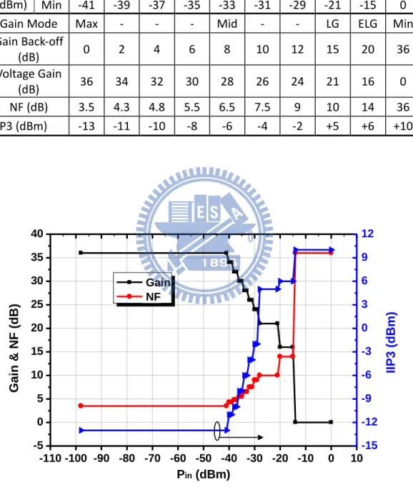
(53) Chapter 3. Receiver System Analysis and Design. Table 3.1 RF front-end gain distribution and their corresponding NF/IIP3 -38 -37 -. -36 -35 -. -34 -33 Mid. -32 -31 -. -30 -29 -. -28 -21 LG. -20 -15 ELG. -14 0 Min. 2. 4. 6. 8. 10. 12. 15. 20. 36. 34. 32. 30. 28. 26. 24. 21. 16. 0. 4.3 -11. 4.8 -10. 5.5 -8. 6.5 -6. 7.5 -4. 9 -2. 10 +5. 14 +6. 36 +10. 40. 12. 35. 9. 30. Gain & NF (dB). -40 -39 -. 25. 6. Gain NF. 3. 20. 0. 15. -3. 10. -6. 5. -9. 0. -12. -5 -110 -100 -90 -80 -70 -60 -50 -40 -30 -20 -10. 0. Pin (dBm). Fig. 3.1. RF front-end gain settings versus input power levels.. 27. -15 10. IIP3 (dBm). Max -98 Pin (dBm) Min -41 Gain Mode Max Gain Back-off 0 (dB) Voltage Gain 36 (dB) NF (dB) 3.5 IIP3 (dBm) -13.
數據
+7

相關文件
三.在高解析度電視尚未普及前, HD攝錄機 也可以轉換成SD格式來拍攝, 仍然能在一 般的寬銀幕或 標準銀幕之電視觀賞HDV 格式的影像.----不過所觀賞到的影像品質 是SD的 畫質。... Sony Digital
根據商務活動之舉辦目標及系統需求,應用 Microsoft Office 文書處理 Word、電子試算表 Excel、電腦簡報 PowerPoint、資料庫 Access
(軟體應用) 根據商務活動之舉辦目標及系統需求,應用 Microsoft Office 文書處理 Word、電子試算表 Excel、電腦簡報 PowerPoint、資料庫 Access
Coat video digital interaction teach
CeBIT is the world's largest trade fair showcasing digital IT and CeBIT is the world's largest trade fair showcasing digital IT and5. telecommunications solutions for home and work
Keyboard, mouse, and other pointing devices; touch screens, pen input, other input for smart phones, game controllers, digital cameras, voice input, video input,. scanners
Beauty Cream 9001, GaTech DVFX 2003.
Blue-screen matting, digital composition, Optical compositing digital composition, digital matte painting. Smith Duff Catmull
