行政院國家科學委員會專題研究計畫 期中進度報告
應用於生物分子檢測與奈米元件之奈米技術平台(1/3)
計畫類別: 個別型計畫 計畫編號: NSC93-2120-M-009-010- 執行期間: 93 年 08 月 01 日至 94 年 07 月 31 日 執行單位: 國立交通大學奈米科技研究所 計畫主持人: 許鉦宗 共同主持人: 梁耕三,洪偉修,李耀坤 報告類型: 精簡報告 處理方式: 本計畫可公開查詢中 華 民 國 94 年 5 月 23 日
國家科學委員會研究計畫--期中精簡報告
應用於生物分子撿測與奈米元件之奈米技術平台(
1/3)
Nanofabrication platform for biomolecular Sensors and
Electronics
計畫編號:NSC 93—2120-M-009-010
執行期限:93 年 8 月 1 日至 94 年 7 月 31 日
主持人:許鉦宗 交通大學奈米科技研究所 E-mail: [email protected]
一、中文摘要 奈米量子元件在過去十多年努力已 漸俱成果的同時,生醫與分子感測也因各 種生命物質化學結構的逐漸了解,在過去 三年蓬勃的發展起來。另一方面,分子電 子學研究於這數年間的掘起也為科學研 究注入另一股活力。除了特定相關知識之 外,這三個方向都必須有賴於可靠的奈米 製程技術之建立。本計畫結合具不同研究 領域(如化學、生化、電機與材料分析) 專長的實驗室,提出一種新的奈米微區圖 形化(patterning)技術,並運用於生物分 子 奈 米 檢 測 機 制 與 奈 米 元 件 電 性 的 研 究;本技術是將反應前驅物(precursors) 導入反應腔,於低溫下在基材(substrate) 上 形 成 吸 附 (adsorption) 與 凝 結 (condensation),再經由 SPM 針端提供的 低能量電子或是光子,激發 SPM 針端下吸 附於基材的前驅物進行分解反應,在基材 表面上形成奈米結構,稱之為掃瞄式探針 激 發 前 驅 物 分 解 沈 積 技 術 , SPM-condensed precursor decomposition(SPM-CPD)。 本計畫基本上包含三個子計畫 (1) 奈米結構製造與其相關化學反應研究:其 主要目的在於利用掃瞄式探針顯微鏡在 矽或不同基材上,激發前驅物進行分解反 應,獲得所需化學成份的奈米結構;因應 生物分子與奈米電子的研究與應用,利用 不同化學前驅物製作不同材料的奈米結 構,如利用含有不同配位基(ligand;如 carbonyl, β-diketonate 或 alkanephosphine)的金屬化合物為前驅 物,可製作高純度的奈米金屬點或奈米 線,另外;亦可利用含 Si 或 Ge 的前驅物, 製作半導體奈米點或奈米線。因掃瞄式探 針顯微鏡所製成之奈米結構的化學成份 或純度,與其化學反應機制相關,亦即取 決於所使用的前驅物化學組成,因此本計 畫將藉由不同的表面分析技術,研究其反 應機制,提供最佳前驅物的製程條件與選 擇。此外,本計畫亦利用同步輻射相關的 顯微術,研究所獲得的奈米結構化學組成 與微結構的分佈。 (2) 奈米元件製作:在上述奈米微 區圖形化技術基礎上,本計畫將製造量子 元件並觀察其量子現象,量子元件的結構 由奈米線奈米點奈米線組成,其中可 經由側閘極改變奈米點的能位以操控該 元件。本計畫亦將研製金屬/半導體之奈 米接面(nanocontacts),這個部分將集中 研究於困擾下一代 IC 製程之鎳矽奈米接 面上。 另一方面本計畫亦將研製奈米線 與微流管結構,使生化物質經由微流管固 化於奈米線表面。經由奈米微區圖形化製 程控制與不同材料的選擇,奈米線的表面 特性可分成兩種:第一種是可全面固化生 化物質於其表面的奈米線;第二種是生化物 質 只 固 化 生 化 物 質 於 局 部 奈 米 線 表 面。經由全面修飾奈米線表面到局部修飾 奈米線表面與奈米線表面積/體積比例的 調整,透過載子於奈米線傳導的現象研 究,了解本元件於特定生化物質感測之終 極靈敏度。 (3) 類固醇奈米檢測元件之蛋白質 工程與化學修飾研究: 此子計畫將於奈米 線 上 接 合 生 物 分 子 以 建 構 奈 米 檢 測 元 件。KSI (∆5 -3-ketosteroid isomerase) 被挑選用以辨識多種類固醇賀爾蒙。數種 新穎的生物技術如:定向演化、定點突變 及表面電漿共振技術等,以篩選具有辨識 特定類固醇能力的蛋白質。先前的研究已 發現一帶有電荷之有機化合物,可標識於 KSI 外環結構上,若將化學標識後之 KSI 固定化於奈米線上則可建構奈米場效電 晶體,當有待測類固醇存在時,有機標識 物會被取代而暴露於奈米線上,此有機標 識物上之電荷會造成奈米線之導電度變 化,藉此反應出類固醇之存在與濃度數 據。 關鍵詞:奈米製造,量子元件,生醫與分 子感測,奈米微區圖形,化掃瞄式探針激 發前驅物分解沈積技術 Abstract
Two nanodevices, nanoflash devices with double floating gates and nanowire sensors, fabricated by scanning probe lithography (SPL) technology and tetramethylammonium hydroxide (TMAH) anisotropic wet etching are demonstrated for the wide-range applications of silicon nanowires. On a (110) SOI silicon wafer, along [001] and [111] directions, a silicon nanowire was generated through local oxidation with SPL followed by wet etching with TMAH solution. Silicon nanowires (SiNW) with profiles of sidewall either sloped or vertical were formed after anisotropic etching in [001] or [111] direction respectively. After deposition of a polysilicon film on the SiNW with LPCVD,
nanostructures of a nanoflash device with polysilicon double-floating side gates were obtained along the [111] part of SiNW after RIE spacer etching. The silicon nanowire channel has width 20 nm and height 200 nm; the width of the self-aligned floating gate is approximately 40 nm. For nanosensors, selective deposition of gold nanoparticles on the surface of SiNWs pretreated with N-(2-aminoethyl)-3-aminopropyl-trimethoxy silane (AEAPTMS) enables detection of molecules. An engineered enzyme, KSI-126C having a terminal thiol, was designed to bind with gold nanoparticles on the surface of SiNW. Shifts of turn-on voltage in I-Vds characteristics are clearly
observable after binding of molecules and gold nanoparticles.
Keywords: silicon nanowires, scanning probe
lithography, TMAH wet etching, spacer, enzyme, gold nanoparticles, AEAPTMS 二、Background and objective
Flash memories have enhanced flexibility relative to read-only memories (EPROM) that are electrically programmable but erasable via ultraviolet (UV) exposure. Because of larger chip area and power consumption, electrically erasable and programmable read-only memories (EEPROM) are adopted for specific applications only. There has been much research on nanoflash devices with high density, small power consumption, and high access speed, but with the dimensions of the floating gate reaching the sub-100-nm range the fabrication process becomes difficult to control. Several fabrication technologies have been developed for floating-gate flash memories. The nanoparticle dots that are embedded in the oxide layer between a control gate and a channel act as floating memory nodes. It is easy to obtain a small floating gate, but the nanoparticles are invariably randomly deposited.1 To generate floating dots for a SOI flash memory device, Tang et al 2 made use of a rate of oxidation on silicon that varies with concentration of
doping. Choi et al. utilized atomic layer doping (ALD) to fabricate a flash memory with a side channel and a side floating gate.3 Futatsugi et al. developed a new Si single-electron memory having an ultra-small floating gate, called a floating dot, stacked on a channel with a self-aligned process; to obtain a narrow channel FET, a line pattern of chloromethyl polystyrene (CMS) resist was formed with width 70 nm and length about 200 nm using electron-beam (EB) lithography.4
Current biological sensing techniques based on electrical detection have been extensively investigated5-8). Biosensors based on electronic detection are easy to integrate and to miniaturize with current IC techniques. It offers an alternative to traditional techniques but the potential has not yet been fully explored. For example, Malaquin’s9) group combined high sensitivity, through the use of nanoscale devices that detected few molecules, with robustness and signal amplification using colloidal labeling. The principle of detection is a modification of the junction surface between two electrodes after molecular immobilization, which induces a measurable alteration of the conductance of the device. Chan’s10) group subsequently
fabricated a micro-DNA array with CMOS-compatibility by modifying the metallization process. After introduction of a double-gold amplification, the sensitivity of the DNA array was evaluated on a picomole scale. Although the sensitivity of the DNA array is still improvable with a decreasing gap between electrodes, a small gap between electrodes causes a short circuit between electrodes after silver enhancement. An electrical biosensor of another type, based on MOSFET and a FET-type charge sensor to detect a DNA sequence, is a semiconductor sensor that measures the variation of electric charge caused by immobilization of DNA on the gate metal (Au). The operating principle is explained on the basis of a self-assembled monolayer (SAM) and MOSFET 11), but the sensitivity and potential for integration are limited. The limitation of sensitivity of biosensor devices fabricated in planar
semiconductors has been recently overcome with SiNW devices12-13).
Here we described the fabrication of a nanoflash device with self-aligned double floating gates and SiNW nanosensors based on a SPL technique and anisotropic TMAH wet etching, and demonstrate the electrical properties of nanoflash devices with double-floating side gates and nanosensors. 三、Experiments
The devices are fabricated on a p-type separation by implantation of oxygen (SIMOX) wafer with silicon 75 nm thick and buried silicon dioxide 350 nm thick. After wafer cleaning, a thermally oxidized SiO2
layer 30 nm thick was formed on the sample surface. The first optical mask was then used to remove thermal oxide to define the active area of a device. Local oxidation was performed by SPL in ambient conditions using a PtIr tip to generate nano oxide patterns along [001] and [111] directions. SiNW were generated with TMAH wet etching solution. A layer of tunneling oxide of thickness 8 nm was also deposited on the SiNW. Subsequently, a polysilicon film of thickness 100 nm was deposited on the SiNW with LPCVD. Nanostructures of a nanoflash device with polysilicon double-floating side gates were obtained in the [111] part of a SiNW after RIE etching. Because sidewalls were slanted, polysilicon on the SiNW was all etched away along the [001] direction. After deposition of nitride with LPCVD as gate dielectric and an aluminum layer, both top gate and source-drain pads were defined by photolithography.
A solution of gold nanoparticles was first prepared by citrate reduction14). The stock solution consisted of hydrogen tetrachloroaurate (HAuCl4·4H2O, 0.026 g)
and DI water (40 mL), and was heated until initiation of boiling. To a trisodium citrate (C6H8O7Na3·2H2O) solution (0.1 M, 100 mL)
was added AuCl4 solution (40 mL) at the
boiling point with vigorous stirring. The solution initially developed a pale yellow
color and then turned grey; eventually it became lavender and then transformed into a dark-wine color. This solution was cooled under continuous stirring. All AuCl4 was
converted to gold particles by this method; the typical concentration of gold nanoparticles solution was from 1.3x10¹¹ particles/cm2 to2.71x1012 particles/cm2. The diameter of gold nanoparticles is controllable in a range 5 – 15 nm with this method. These gold nanoparticles are citrate-coated with negative charge.
SiNW devices were adopted to detect molecules in our experiment. The SiNW were fabricated as follows, beginning with a wafer of p-type, (100)-oriented silicon on an insulator (SOI) that had a buried isolation oxide layer formed with implanted oxygen (SIMOX). The thickness of the silicon-on-insulator layer is 50 nm and that of the buried isolation oxide layer is 200 nm. The SOI wafer was cleaned with a standard RCA cleaning process. The silicon-on-insulator layer was then thinned by dry oxidation, to decrease the silicon thickness to 10 ~ 12 nm. The first mask was then introduced to define active areas on the oxide layer. Scanning-probe lithography was used to produce nano-oxide patterns with an etching mask in the tetramethylammonium hydroxide (25 % by mass) wet etching process to fabricate the silicon nanowires. Then a layer of oxide (thickness 8 nm) was grown on the surface of the SiNW. After a layer (thickness 500 nm) of aluminium was deposited, source-drain aluminium contact pads connected through the SiNW were defined with photolithography.
Formation of self-assembled monolayers (SAM) provides an easy route to surface functionalization15) by organic molecules containing suitable functional groups such as –SH, –CN, –COOH, –NH2
and silanes on a selected metallic or semiconducting surface. In this work we further modified the hydroxyl-terminal surface of SiNW with a silanization
procedure involving N-(2-aminoethyl)-3-aminopropyl-trimethoxy
silane (AEAPTMS), which provides a surface bearing a free amino (-NH2) group
that becomes involved in a coulombic interaction with negatively charged Au nanoparticles. In the procedure for silanization and deposition of gold nanoparticles, after cleaning the SiNW in acetone and 2-methylpropan-1-ol with ultrasonic agitation, the devices were immersed in an AEAPTMS solution (2.2 mM), diluted with water, for 5 min. The commercially available silane coupling agent, AEAPTMS, was used without further purification. The samples were then dried with a nitrogen gun and baked at 120 °C for 30 min on a hotplate. The AEAPTMS-treated samples were then immersed in a solution of gold nanoparticles for 1 h. Afterwards, samples were rinsed with distilled water and dried with a nitrogen gun. The coulombic interaction between amino groups and the negatively charged surface of gold nanoparticles immobilizes the gold nanoparticles on the silane-coupler treated SiNW16). Many researchers have attempted to functionalize biomolecules such as DNA17) or protein18) with a thiol group. In
this work we engineered KSI-126C with a thiol group as a thiol terminal of a biomolecule that can readily replace the citrate ion and bind onto a surface of gold nanoparticles with covalent bonds. We then measured he electrical properties of SiNW after binding KSI-126C.
IV. Results and Discussions
Oxide patterns formed on the silicon surface by SPL served as a mask for wet etching with TMAH solution. Fig. 3(a) shows AFM and SEM images of a SiNW channel of a nanoflash device. The inset shows a SiNW of width 20 nm and height 200 nm obtained along the [111] crystal direction after TMAH wet etching. Fig.3 (b) shows a SEM image of a SiNW channel with double floating side gates fabricated after RIE polysilicon spacer etching. The tetramethylamonium ions (TMA+) from the
dissociation of TMAH apparently decrease rates of etching of high index crystallographic planes. TMA+ adsorbed on these high-index crystallographic planes and hindered access of the etching agent (OH -ions) to the surface.7 As shown in the inset of Fig. 1(a), slant planes invariably form at the bottom of a vertical channel sidewall. As shown in Fig. 1(b), floating gates formed only at the region of a vertical sidewall of a SiNW. Polysilicon coated along [001] was all etched away after RIE etching. The floating gates formed at sidewalls of a SiNW along [111] have width 40 nm and length 500nm. With a structure of double floating side gates, they are electrically coupled with the channel of a SiNW. Changes in the source or drain current due to charging/discharging (programming/erase) of floating gates are to be expected.
When electrons tunnel into floating gates (programming),the sidewalls of p-type SiNW accumulate such that the conductivity of the SiNW increases, whereas when electrons are pumped out from the floating gates (erasure), the conductivity of SiNW decreases. Figure 4(a) shows the Ids–Vds
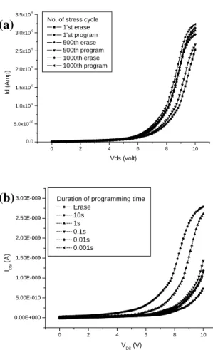
characteristics of nanoflash memory devices when Vds was swept from 0 V to 8 V. During
programming, a bias +20 V was applied to the control gate and a bias -10 V to the drain. Programming results in electrons tunnelling from the channel to floating gates according to the Fowler-Nordheim (FN) mechanism. For erasing, a bias -20 V was applied to the control gate and a bias +10 V to the drain to pump electrons from the floating gates. As depicted in Fig. 2(a), operation window narrowing was observed in the I-V characteristics of a nanoflash device after that device was programmed and erased up to 1000 times. The duration of each program is 10 s. Operation window narrowing effect is expected to reduce if silicon nitride was replaced by the silicon oxide in the process.
When Vds was operated at 8 V, the drain
current on/off ratio is approximately 7. Fig. 2(b) shows characteristics of the nanoflash with respect to duration of program. A
decreased duration of program resulted in a decrease of tunneling electrons into the floating gate such that a smaller conductance was observed, but a difference between on/off currents is still clearly identified even with duration of programming down to 0.001 s.
Based on highly sensitive of electrical property of SiNW, we expected a variation of electrical conductance of SiNW when molecules bind to gold nanoparticles on the surface of SiNW. AEAPTMS modified the silicon dioxide layer by reacting with silanol groups to generate an amino-derivatized surface, which changed the surface potential of SiNW from negative to positive and resulted in a decreased conductance. The gold nanoparticles are bound to amino groups on the surface of SiNW subsequently, and the citrate-coated gold nanoparticles act as negative gates. Hole accumulation in SiNW is expected to cause an increased electrical conductance of p-type SiNW. Fig. 3a shows the dynamic variation of conductance as gold nanoparticles were added onto an AEAPTMS-pretreated surface of SiNW. The conductance increases sharply right after gold nanoparticles are supplied. The bias voltage on a SiNW was maintained at 500 mV during the measurement. That the conductance of SiNW became stable in 500 s after the supply of gold nanoparticles indicates that the reaction became saturated. Figure 3b shows a SEM image of gold nanoparticles anchored on a SiNW after supply of gold nanoparticles for 1 h.
Aminosilane immobilization appears to have a strong effect on the turn-on voltage of SiNW. When the turn-on current (Ids) of the
SiNW device was chosen to be 1 nA, the turn-on voltage of the SiNW shifted from –2.7 volts to –8.1 volts after modification with AEAPTMS. This shift in the turn-on voltage results from the substitution of the hydroxyl terminal with amino groups on the surface of SiNW. For p-type SiNW, the shift of the turn-on voltage occurs because of decreased charge density of a negatively charged surface on binding by AEAPTMS molecules that contain
positively charged amino groups in solution. When the gold nanoparticles were supplied and functionalized with amino groups on the surface of SiNW, the Id-Vg curve showed
another shift in turn-on voltage, from –2.7 V to –3.2 V. The reason is that gold nanoparticles bind with only amino groups and became saturated on the surface of SiNW. The gold nanoparticles with negative citrate charges on the surface of SiNW worked like a negative-gate bias, resulting in an accumulation of holes in SiNW (turn-on voltage = -3.2 V). Because of the distance effect, the impact of a negative charge field effect on the conductance of SiNW with gold nanoparticles is expected to be smaller that that of hydroxyl groups. Enzyme KSI-126C molecules with thiol terminals were supplied and bound with gold nanoparticles on the surface of SiNW. The IV curve again demonstrated a shift of turn-on voltage from -3.2 V to -0.2 V. Figure 4 shows the conductance properties. Although details of the binding of enzyme require clarification, the electrical measurements showed that more negative charges were introduced onto the surface of SiNW such that their conductance increased through the negative charge field effect. The electrical conductance measurements indicate that the field effect of SiNW is induced on binding of molecules, and nanoparticles on SiNW can be detected with great sensitivity. These electrical properties are in accordance with the polarity of charges due to surface modifications of SiNW by AEAPTMS, gold nanoparticles and KSI-126C. Details of the surface chemical structure and binding mechanism on SiNW require further clarification.
To ensure the silanization of AEAPTMS on the patterned oxide surface, surface analysis techniques like XPS and PEEM were conducted to check the Nitrogen and carbon signals. Figure 5(a) shows surface chemical structure of the sample for XPS analysis. Nitrogen can be detected on the XPS spectrum of AEAPTMS SAM on the SiO2
surface for immersion of samples in different concentration of AEAPTMS, as shown in
Fig. 5(b). Figure 5(c) shows the patterned the carbon K edge signal on the patterned SiO2 for AEAPTMS. These results support that binding of AEAPTMS on the oxide surface. V. CONCLUSIONS
A self-aligned technology for nanoflash devices with double floating gates is reported using scanning probe lithography and anisotropic wet etching. On a (110) SOI silicon wafer, along [001] and [111] directions, a silicon nanowire was generated with local oxidation by SPL followed by wet etching with tetramethylammonium hydroxide (TMAH) solution. Polysilicon self-aligned floating gates of width approximately 40 nm and length 500 nm were fabricated. Programming and erasing of the nanoflash device were performed, and an on/off current ratio up to 7 was obtained. The fabricated nanoflash device with duration of programming down to 0.001 s still demonstrated the electrical features of memory. Also, selective deposition of gold nanoparticles on an AEAPTMS-pretreated SiO2/Si surface has been demonstrated. Gold
nanoparticles deposited on the oxide surface of SiNW served as linkers to detect molecules. Silicon nanowires were fabricated with scanning-probe lithography and a TMAH wet etching process on a (100)-oriented p-type SOI wafer. These SiNW (10 μm long, 60 nm wide, and 10 nm high) were connected to the electrodes of a source and a drain. The silicon dioxide surface of SiNW was then modified with AEAPTMS into a protein-bindable environment. The silanol group becomes replaced by amino groups on AEAPTMS treatment that causes the surface potential of the SiNW to alter from negative to positive, resulting in a decreased conductance of SiNW. Furthermore, treatments of the surface of SiNW with gold nanoparticles and KSI-126C molecules resulted in shifts of turn-on voltages of SiNW, such that conductance of SiNW was modulated through the charges of bound nanoparticles and molecules. The selective deposition of
gold nanoparticles on SiNW is believed to be useful in both nanoelectronic and nanobiosensing applications.
VI、Acknowledgements
This program is supported by the National Science Council under the contract number NSC 93-2120-M-009-010.
References
[1] Winkler, F. Merget, M. Heuser, B. Hadam, M. Baus, B. Spangenberg, H. Kurz, Microelectronic Engineering, Vol. 61– 62, 497, 2002.
[2] X. Tang, X. Baie, J.P. Colinge , A. Crahaya, B. Katschmarsyj , Solid-State Electronics, Vol. 44, 2259, 2000.
[3] Hoon Choi, Tadao Tanabei, Noriyuki Kotaki, Kwang Wook Koh, Jeoung Chill Shim, Jpn. J. Appl. Phys. Vol. 42, 3361, 2003.
[4] Toshiro Futatsugi, Anri Nakajima, Hiroshi Nakao, FUJITSU Sci. Tech. J., Vol. 34, 142, 1998.
[5] J. I. Hahm, C. M. Lieber, Nano Lett., 4 (2004), 51.
[6] Z. Li, Y. Chen, X. Li, T. I. Kamins, K. Nauka, and R. S. Williams, Nano lett., 4 (2004), 245.
[7] X. C. Zhou, S. J. O’Shea and S. F. Y. Li, Chem. Commun., (2000), 953.
[8] X. Su, S. F. Y. Li and S. J. O’Sheaa, Chem. Commun., (2001), 755.
[9] L. Malaquin, C. Vieu, M. Geneviève, Y. Tauran, F. Carcenac, Microelectronic Engineering, 73–74 (2004), 887.
[10] J. Li, M. Xue, Z. Lu, Z. Zhang, C. Feng, and M. Chan, IEEE Trans. Electron Devices, 50 (2003), 2165.
[11] D. S. Kim, Y. T. Jeong, H. J. Park, J. K. Shin, Biosensors and Bioelectronics, 20 (2004), 69.
[12] P. G. Collins, M. S. Arnold, P. Avouris, Science, 292 (2001), 706.
[13] Y. Cui, C. M. Lieber, Science, 291 (2001), 851.
[14] Frens, G. Nature, 241 (1973), 20.
[15] A. Ulman, Chem. Rev., 96, (1996), 1533. [16] T. Sato, D. G. Hasko, H. Ahmed, J. Vac.
Sci. Technol. B, 15 (1997), 45.
[17] Hainer Wackerbarth Rodolphe Marie,
Mikala Grubb Jingdong Zhang, J. Solid State Eletrochem (2004) 8: 474.
[18] M. T. Klem, D. Willits, M. Young, and T. Douglas, J. Am. Chem. Soc. 125 (2003), 10806.
(a)
(b)
Fig. 1. (a) AFM and SEM images of a SiNW channel of a nanoflash device after TMAH wet etching. The inset shows a SiNW of width 20 nm and length 200 nm obtained along the [111] crystal direction after TMAH wet etching. (b) SEM image of a nanoflash device with double-floating side gates with width about 40 nm and length 500 nm.
0 2 4 6 8 10 0.0 5.0x10⁻¹⁰ 1.0x10⁻⁹ 1.5x10⁻⁹ 2.0x10⁻⁹ 2.5x10⁻⁹ 0x10-9 3.5x10⁻⁹ Id (A mp ) Vds (volt) No. of stress cycle
1'st erase 1'st program 500th erase 500th program 1000th erase 1000th program 3. (a) 0 2 4 6 8 10 0.00E+000 5.00E-010 1.00E-009 1.50E-009 2.00E-009 2.50E-009 00E-009 IDS (A ) VDS (V) Duration of programming time
Erase 10s 1s 0.1s 0.01s 0.001s
Fig. 2. (a) Operation window narrowing was observed in I-V characteristics of a nanoflash device after the device was programmed and erased up to 1000 times; the duration of programming was 10 s. (b) I–V characteristics of a nanoflash device programmed using pulses of varied duration.
0 500 1000 1500 2000 2500 3000 0.0 5.0x10⁻⁸ 1.0x10⁻⁷ 1.5x10⁻⁷ 2.0x10⁻⁷ 2.5x10⁻⁷ 3.0x10⁻⁷ ID (A) Time (s)
Add the gold nanoparticles solution (b)
(a)
(b
3.
(b)
Fig. 3. (a) Dynamic conductance
measurement of a SiNW on binding of gold nanoparticles. (b) SEM image of a SiNW after reaction of gold nanoparticles with an AEAPTMS-pretreated SiNW surface for 1h.
Fig. 4. Ids-Vg curves of a SiNW after binding
turn-on voltage altered from -2.7 V to -8.1 V to -3.2 V and to -0.2 V after binding of AEAPTMS, gold nanoparticles and enzyme
KSI-126C, respectively. Fig. 5. (a) Surface chemical structure of samples for XPS analysis. (b) The XPS spectrum for different samples immersion in different concentration of AEAPTMS for different period of time. All samples show the signal of nitrogen. (c) The C k-edge signal for patterned AEAPTMS. The image is obtained after subtraction of background carbon signal and the effect on surface topograpgy.
研究成果
國際期刊論文:1. Hwang Z. H., Hwang J. M., Hung W. H., and Hwang, H. L. (2004) “Electrodeless Wet Etching of GaN Assisted with Chopped Ultraviolet Light”, Appl. Phys. Lett. 84 3759-3761. (SCI: 4.049)
2. Huang, S-H, Shih, Y-C, Wu, C-Y, Yuan, C-J, Yang, Y-S, Li, Y-K, Wu TK (2004) “Detection of serum uric acid using the optical polymeric enzyme biochip system” Biosensors & Bioelectronics 19, 1627-1633 (SCI: 2.947)
3. Yeh C. C., Lai Y. H., Chu W. Y., Yeh C. T., and Hung W. H., (2004) Photon-Induced Chemical Deposition of Molybdenum on the Platinum Surface, Surf. Sci. 565, 81-88. (SCI: 2.063)
4. Lay T.S., Kuo W. T., Chen L.P., Lai Y. H.,
Hung W. H., Wang J. S., Chi J. Y., Shih D.
K., Lin H. H., (2004) Probing the Electronic Structures of III-V-Nitride Semiconductors by X-ray Photoelectron Spectroscopy, J. Vac.
Sci. Technol. B. 22 1491-1494. (SCI: 1.600)
5. Hwang J.M., Ho K.Y., Hwang Z.H., Hung W.
H., Lau K. M., Hwang H. L., (2004)
Efficient wet etching of GaN and p-GaN assisted with chopped UV source,
Superlattices and Microstructures 35, 45-57.
(SCI: 0.604)
6. Hwang J. M., Hung W. H., and Hwang H. L., (2004) Bias-assisted Activation of p-GaN at Low Temperature in Air”, Phys. Stat. Sol.
(C), 1, 2470-2473.
7. Chen, Y-Y., Cheng C-Y., Haung. T-L. and Li,
Y-K * (2004) “Chitosanase from
Paecilomyces lilacinus with binding affinity
(b) 290 eV Topography subtraction (c) Si substrate SiO2 NH Si O O O (a) NH2 NH Si O O O NH2 NH Si O O O NH2 NH Si O O O NH2
for specific chitooligosaccharides”
Biotechnol. Appl. Biochem. (SCI: 1.034)
8. F. M. Pan, C. Y. Chen, Y. B. Liu, Y. Chang and J. T. Sheu (2004), “Selective growth of carbon nanotubes on scanning probe tips microwave plasma chemical vapor deposition,” J. Vac. Sci. Technol. B 20(6), Jan./Feb., 90-93. (SCI: 1.6)
9. J. T. Sheu, G. M. Kao, K.S. You, and C. C. Chen (2004),” Fabrication and Electrical Properties of Silicon Nanowires”,
Microelectronic Engineering, Vol 73-74,
594-598. (SCI: 0.9)
10. K. M. Chang, K.S. You, J. H. Lin, and J. T.
Sheu (2004), “Alternative process for silicon
nanowire fabrication with scanning probe lithography and wet etching system”, J.
Electrochem. Soc. Vol. 151, G679~G682.
(SCI: 2.2)
11. J. T. Sheu, C. C. Chen, K.S. You, and C. H. Wu (2004), “Nanoflash Device with Self-Aligned Double Floating Gates Using the Scanning Probe Lithography and TMAH Wet Etching”, J. Vac. Sci. Technol. B. Vol. 22, 3154~3157. (SCI: 1.6)
12. J. T. Sheu, C. C. Chen, P. C. Huang, Y. K. Lee and M. L. Hsu, “Selective Deposition of Gold Nanoparticles on SiO2/Si Nanowires for Molecular Detection,” Japanese Journal of Applied Physics, Part 1, Vol.44, No. 4B, pp.2864-2867, 2005. (SCI )
13. J. T. Sheu, C. C. Chen, P. C. Huang, and M. L. Hsu, “Selective Deposition of Gold Nanoparticles on SiO2/Si Nanowire,” Journal of Microelectronic Engineering, Vol 78-79, pp 294-299, 2005. (SCI)
國外會議論文:
1
1.. Wang K.W., Chung S. R., Hung W. H., and Perng T. P. (2004) Desorption of Surfactant and Sintering of Surface Modified PdxNi1-x Nanoparticles,
Technical Proceedings of the 2004 NSTI Nanotechnology, 3, 402-405 2. CChhiihh--YYuu CChheenngg,, CChhuu--HHaann CChhaanngg aanndd Y Yaaww--KKuueenn LLii ((22000044) “) GGeennee AAnnaallyyssiiss a anndd ssiittee--ddiirreecctteedd mmuuttaaggeenneessiiss ssttuuddyy ooff A Assppeerrggiilllluuss FFaammiillyy 7755 E Ennddoo--cchhiittoossaannaassee”” 22nd International Carbohydrate symposium, Scotland, UK 3. Sheng-Wen Liu,, CChhii--YYuu CChheenngg,, Chun-Hung Lin aanndd YYaaww--KKuueenn LLii ( (22000044)) “EExxpprreessssiioonn,, MMuuttaaggeenneessiiss aanndd t thheeaaccttiivveessiitteeaaffffiinniittyy--llaabbeelliinnggooffhhuummaann --LL--ffuuccoossiiddaassee”” 22nd International Carbohydrate symposium, Scotland, UK. 4. J. T. Sheu, C. C. Chen, K. S. You, and S.
T. Tsai (2004), “Nanoflash Device with self-aligned double floating gates using scanning probe lithography and TMAH wet etching,” 48th
Electron, Ion, Photo Beam, Technology and Nanofabrication (EIBPN), San Diego, USA.
5. J. T. Sheu, C. C. Chen, S. C. Lin (2004), “Characteristics of Silicon Nanowires in Biological Molecules Detection,” 48th
48th Electron, Ion, Photo Beam,
Technology and Nanofabrication (EIBPN), San Diego, USA.
6. J. T. Sheu, C. C. Chen, P. C. Huang, and M. L. Hsu (2004), “Selective Deposition of Gold Nanoparticles on SiO2/Si Nanowire,” Micro- and Nano- Engineering (MNE), Rotterdam, The
Neitherlands.
7. J. T. Sheu, C. C. Chen, P. C. Huang, and M. L. Hsu (2004), “Selective Deposition of Gold Nanoparticles on SiO2/Si Nanowire for Molecular Detection,”
Solid State Devices and Materials (SSDM), Tokyo, Japan.
8. J. T. Sheu, T. Y. Tseng, and C. H. Wu (2004), “Fabrication of nano-scaled alumina template mask by using self-assembly anodic oxidation method,” 4th WSEAS Int. Conf. on
Nanoelectronics and Nanotechnology, Jan,
13~15, 2004.
9. J. T. Sheu, C. H. Wu, H. H. Liu , W. H. Hung and T. S. Chao, “UV light Induced Production of Gold nanoclusters on a N-type Silicon Nano-wires by Using Dip Pen Lithography Technique”, EIPBN 2005, May 31-June 3, Orlando, 2005.
10. J. T. Sheu, C. H. Wu , H. H. Liu, and T. S. Chao, “Nano-scale patternning on the silicon oxide surface by using dip-pen nanolithography”, IEEE Nano 2005, Japan, July, 2005.
11. J. T. Sheu, S. P. Yei, S. T. Tsai, and C. H. Lien, “Fabrication and Electrical Transport Properties of Nickel Monosilicide Nanowires”, IEEE Nano 2005, Japan, July, 2005.