國 立 交 通 大 學
電信工程學系
碩 士 論 文
應用於功率管理單元且具無突波回授切換偵測電路之低功
率延遲鎖定迴路式時脈產生器
A Glitch-Free and Low-Power DLL-Based Clock Generator
Using a Feedback Switching Detector for Power Management
Systems
研究生:林鼎國
指導教授:闕河鳴 博士
率延遲鎖定迴路式時脈產生器
A Glitch-Free and Low-Power DLL-Based Clock Generator
Using a Feedback Switching Detector for Power
Management Systems
研 究 生:林鼎國 Student: Ding Guo Lin 指導教授:闕河鳴 博士 Advisor: Dr. Herming Chiueh
國 立 交 通 大 學
電 信 工 程 學 系
碩 士 論 文
A Thesis
Submitted to Department of Communication Engineering College of Electrical and Computer Engineering
National Chiao Tung University in Partial Fulfillment of the Requirements
for the Degree of Master of Science in Communication Engineering Apr. 2010 Hsinchu, Taiwan 中 華 民 國 九 十 九 年 四 月
應用於功率管理單元且具無突波回授切換偵測電路之低功
率延遲鎖定迴路式時脈產生器
研究生:林鼎國 指導教授:闕河鳴 博士 國立交通大學 電信工程學系碩士班摘要
功率管理單元可以根據系統的操作狀況來動態調整系統操作頻率以及系統 操作電壓以達到降低系統平均功率消耗的目的,像是Intel 的 speedstep 技術就含 有六種操作電壓/頻率組合,這類型的功率管理單元需要一個可程式化的時脈產 生器來提供可變的操作頻率。 本論文提出一個可抑制變頻切換突波與大鎖定範圍的延遲鎖定迴路式時脈 產生器,架構中使用了回授切換偵測器取代多組相位偵測器加電流幫浦的架構來 抑制變頻切換突波,相較於使用多組相位偵測器加電流幫浦的架構可以有效地降 低晶片面積,此時脈產生器的輸出頻率範圍為100MHz 到 1.6GHz,並且提供八 階的操作頻率階級;量測結果顯示當系統操作在 1.6GHz 時鋒對鋒抖動量為 23.316ps、功率消耗為 37.8mW。 最後的版本則是將量測所發現的問題做修正並且重新設計邊緣合成器,在修 正過後將系統輸出範圍提昇至 1.8GHz,這些改進使得此系統更適合使用於功率 管理單元。A Glitch-Free and Low-Power DLL-Based Clock Generator
Using a Feedback Switching Detector for Power
Management Systems
Student: Ding-Guo Lin Advisor: Dr. Herming Chiueh
SoC Design Lab, Department of Communication Engineering,
College of Electrical and Computer Engineering, National Chiao Tung University Hsinchu 30010, Taiwan
Abstract
A power management system can ensure system to operate within specification and achieve nominal power dissipation through power/speed modulation. For example, Intel Pentium M processor has speedstep technology which has six frequency/voltage modes to switching. For such power management system, we need a programmable clock generator to provide various operation frequencies.
In this thesis, a glitch-free DLL-based clock generator using a feedback switching detector is proposed for a programmable power management system. The proposed circuitry utilizes feedback switching detector to eliminate undesired glitch problem which is generated by switching feedback stage of DLL. The output frequency range is from 100MHz to 1.6GHz with 8 steps for operation frequency. The power consumption is 37.8mW and P-P jitter is 23.316ps at 1.6GHz.
After measurement we fix the problem found in measurement and revise edge combiner. The revise extends output frequency range to 1.8GHz. The improvements make this work more suitable for a power management system.
Acknowledgments
首先,我要感謝指導教授闕河鳴博士,在整個碩士班的過程當中,不只給予 我許多專業知識上的指導,使我在整個研究的過程中可以解決許多困難,並在最 後完成此專題的研究。在平日的報告會議中,也在老師身上學到許多報告與文件 格式的技巧。在論文的撰寫過程中也給予我不斷的協助與建議,使得此論文得以 順利的完成。 再來要感謝實驗室的嘉儀、秉勳、凱迪、品翰、明君、春慧學長姐,平常在 課業上以及生活上的幫助,讓我可以很快的融入碩士班以及實驗室的環境中。 在整個研究生活中,幸虧有實驗室同學是瑜、國哲、鎮宇、燦杰還有實驗室 學弟登政以及高中的好朋友們宜旻、國任、劉為、以軒的扶持與幫助,讓我的碩 士班生活過的非常充實與快樂,並且順利的完成碩士班學業,謝謝你們。 最後,我要感謝我的父母、家人,無論是在心理上或經濟上都給予我最大的 支持,使我能專心致志的完成碩士班學業。林鼎國
Apr. 2010
Contents
中文摘要
...
I
English Abstract
...
II
Acknowledgments
...
III
Contents
...
IV
List of Tables
...
VI
List of Figures
...
VII
Chapter 1 Introduction……….1
1.1 Project Motivation and Research Goals………...……….1
1.2 Thesis Organization………...………2
Chapter 2 The Basic and Design Challenges of DLL-Based Clock
Generator………..………..3
2.1 The Basics of the DLL-Based Clock Generator………...………….3
2.2 Design Challenges of DLL-Based Clock Generator…..…...……...…5
2.3.1 Multiplication Factor Issue………..6
2.3.2 Locking Issue………...14
2.3.3 Wide Range Locking Issue………..16
2.3 Design Concepts and Design Goal………...……..17
Chapter 3 Target Circuit/System Implementation ………...19
3.1 System Architecture………19
3.2 Control Circuit……….20
2.3.1 Multiplication Factor Controller ………20
2.3.2 Feedback Switching Detector .………...21
2.3.3 Glitch-free lock detector ………..23
3.3 PFD …….……….27
3.4 CP and LF………28
3.5 Pulse Reshaper ……...………29
3.6 Delay Cell………31
Chapter 4 Simulation and Measurement Results…………...…….……..37
4.1 Locking Range Simulation………..37
4.2 Whole System Simulation……….40
4.2.1 2008 Work Post-Layout Simulation….………40
4.2.2 2009 Work Post-Layout Simulation….………42
4.3 Measurement Setup……...………..49
4.4 Measurement Results ……….52
4.4.1 Measurement results of 2008 Work………40
4.4.2 Measurement results of 2009 Work………40
4.5 Performance Summary………… ………57
Chapter 5 Conclusion and Future Works…………..………...60
5.1 Conclusion………...60
5.2 Future Works………...61
List of Tables
Table 1.1 Performance states for the Intel® Pentium® M processor at 1.6GHz...1
Table 3.1 Enable signal pattern………21
Table 3.2 Lock detector work example when feedback stage is VCDL’s stage 8...25
Table 3.3 Each Status phase difference region……….27
Table 3.4 Logic gates’ size in edge combiner ……….36
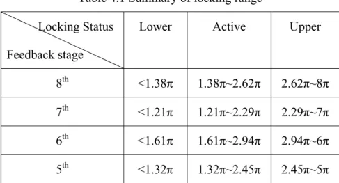
Table 4.1 Summary of locking range………...40
Table 4.2 Performance of 2008 work post layout simulation...………42
Table 4.3 Performance of 2009 work post layout simulation………...…...49
Table 4.4 Performance Summary of 2008 work………...54
Table 4.5 Performance summary of 2009 work………..……….57
Table 4.6 Power consumption at each output frequency………..57
Table 4.7 Comparison between 2008 and 2009 work……….58
List of Figures
Fig. 2.1 DLL clock generator concept………..4
Fig. 2.2 Conventional DLL based clock generator………...5
Fig. 2.3 Simplified edge combiner in [4]………..7
Fig. 2.4 Phase diagram in [4]………8
Fig. 2.5 Simplified example of [5]………...8
Fig. 2.6 The edge combiner in [7]………...9
Fig. 2.7 Pulse toggle method………10
Fig. 2.8 The edge combiner in [8]………..10
Fig. 2.9 Example of 50% and not 50% duty cycle………11
Fig. 2.10 The idea of phase blender………...12
Fig. 2.11 Block diagram of [6]………...12
Fig. 2.12 Undesired glitch………13
Fig. 2.13 Block diagram of [2]………13
Fig. 2.14 Locking range of conventional PD………..15
Fig. 2.15 CP and LF………16
Fig. 2.16 PD gain curve………17
Fig. 3.1 Project system architecture of DLL based clock generator……….19
Fig. 3.2 Rising edge trigger………22
Fig. 3.3 Falling edge trigger……….22
Fig. 3.4 Feedback switching detector………...22
Fig. 3.5 Feedback switching detector working example………..23
Fig. 3.6 Original type lock controller………24
Fig. 3.7 Example of lock detector when feedback stage is 8th stage of VCDL………25
Fig. 3.9 Modified lock controller……….26
Fig. 3.10 PFD’s schematic………28
Fig. 3.11 Charge Pump……….28
Fig. 3.12 Pulse reshaper………....29
Fig. 3.13 Signal go through pulse reshaper………30
Fig. 3.14 Characteristic plot of PFD, CP and control circuit when feedback stage is 8 … … … 3 0 Fig. 3.15 Characteristic plot of PFD, CP, pulse reshaper and control circuit when feedback stage is 8………30
Fig. 3.16 Current mode delay cell………...31
Fig 3.17 2008 work Delay Range of VCDL………32
Fig 3.18 2009 work Delay Range of VCDL………...32
Fig. 3.19 Edge Combiner……….34
Fig. 3.20 TPL circuit………..34
Fig. 3.21 Simplified Edge Combiner………35
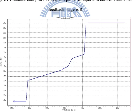
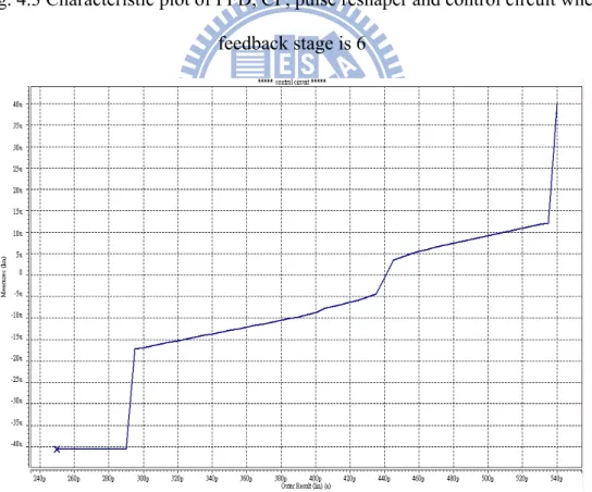
Fig. 4.1 Characteristic plot of PFD, CP, pulse reshaper and control circuit when feedback stage is 8……….38
Fig. 4.2 Characteristic plot of PFD, CP, pulse reshaper and control circuit when feedback stage is 7………..38
Fig. 4.3 Characteristic plot of PFD, CP, pulse reshaper and control circuit when feedback stage is 6……….39
Fig. 4.4 Characteristic plot of PFD, CP, pulse reshaper and control circuit when feedback stage is 5……….39
Fig. 4.5 Eye diagram of input clock is 400MHz and multiplication factor is 4……...40
Fig. 4.6 Eye diagram of input clock is 300MHz and multiplication factor is 4……...41
Fig. 4.8 Eye diagram: Reference clock is 450MHz and multiplication factor is 4…..43
Fig. 4.9 Eye diagram: Reference clock is 450MHz and multiplication factor is 3.5...43
Fig. 4.10 Eye diagram: Reference clock is 450MHz and multiplication factor is 3....44
Fig. 4.11 Eye diagram: Reference clock is 450MHz and multiplication factor is 2.5.44 Fig. 4.12 Eye diagram: Reference clock is 450MHz and multiplication factor is 2....45
Fig. 4.13 Eye diagram: Reference clock is 450MHz and multiplication factor is 1.5.45 Fig. 4.14 Eye diagram: Reference clock is 450MHz and multiplication factor is 1…46 Fig. 4.15 Eye diagram: Reference clock is 450MHz and multiplication factor is 0.5.46 Fig. 4.16 VCTRL at each feedback stage………47
Fig. 4.17 Eye diagram: Reference clock is 450MHz and multiplication factor is 4....48
Fig. 4.18 Eye diagram: Reference clock is 350MHz and multiplication factor is 4…48 Fig. 4.19 Eye diagram: Reference clock is 250MHz and multiplication factor is 4…49 Fig. 4.20 2008 Work Die Photo……….…...50
Fig. 4.21 2009 Work Die Photo………...…….…………...50
Fig. 4.22 2008 Work Prototype PCB……….………..50
Fig. 4.23 2009 Work Prototype PCB..……….51
Fig. 4.24 2008 Work Measurement environment..………..….51
Fig. 4.25 2009 Work Measurement environment……….51
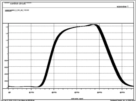
Fig. 4.26 Eye [email protected], P-P Jitter : 23.316ps, Population : 13124…….….52
Fig. 4.27 Eye [email protected], P-P Jitter : 24.168ps, Population : 12804………..52
Fig. 4.28 Eye [email protected], P-P Jitter : 9.065ps, Population : 12804………....53
Fig. 4.29 Eye [email protected], P-P Jitter : 21.404ps, Population : 10005……….53
Fig. 4.30 Eye [email protected]...…55
Fig. 4.31 Eye [email protected]...….56
Fig. 4.32 Eye [email protected]…...56
Chapter 1
Introduction
1.1 Project Motivation and Research Goals
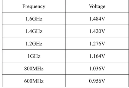
A power management system can ensure system to operate within specification and achieve nominal power dissipation through power/speed modulation [1]. For example, Intel Pentium M processor has speedstep technology which has six frequency/voltage modes to switching [2]. In [2] we can find that Intel Pentium M processor support 6 operation frequency and supply voltage operation points for different work states as shown in Table 1.1.
Table 1.1 Performance states for the Intel® Pentium® M processor at 1.6GHz
Frequency Voltage 1.6GHz 1.484V 1.4GHz 1.420V 1.2GHz 1.276V 1GHz 1.164V 800MHz 1.036V 600MHz 0.956V
For such application, we need a programmable, wide frequency range clock generator to provide various operation frequencies. Our lab had designed a DLL based clock generator[3] for this purpose. Previous work use multi-PFD-CPs to solve undesired glitch, but multi-PFD-CPs structure costs too much chip area.
The project goal is to design a DLL based clock generator which can provide programmable frequency-switching function and wide output frequency range. This work also has to have various frequency multiplication factors for 6 or more operation points. Besides, a new circuit is needed to replace multi-PFD-CPs and to solve undesired glitch. Without using multi-PFD-CPs structure we can lower the chip area.
1.2 Thesis Organization
Chapter 2 will introduce the basic of DLL based clock generator. After that the design challenges of DLL based clock generator will be mentioned. In the end of this chapter the design concept in this project will be presented.
Chapter 3 begins at introduction of this DLL based clock generator’s structure. The rest of this chapter will describe the detail of each sub-circuit.
Chapter 4 contains whole system’s simulation results. And the measurement settings of the DLL-based clock generator and the measurement instruments are introduced later. Then the measurement results of 2008 work are shown. After measurement we find out some problems and we fix problems at 2009 work DLL based clock generator. So the final part of this chapter is simulation results of 2009 work DLL based clock generator.
Chapter 5 is the final chapter of this thesis. This chapter presents conclusion and future work.
Chapter 2
The Basic and Design Challenges of
DLL-Based Clock Generator
The basic of DLL based clock generator is illustrated at beginning of this chapter. And the design challenges of DLL based clock generator are described later. Final part of this chapter will be the design concept and goal of this project.
2.1 The Basic of the DLL-Based Clock Generator
Delayed lock loop-based clock generator has several inherent advantages by using low jitter crystal oscillator as reference clock. We expand this concept more precisely by Fig 2.1. Reference clock feeds in voltage control delay line which total delay time is locked at one time period of reference clock. The delay elements produce several equally spaced edges within one reference clock’s time period. Then edge combiner uses these edges to generate desired output frequency. Unlike PLL uses voltage control oscillator which have jitter accumulation problem, DLL jitter accumulates only within one time period of reference clock. If we use a high Q and low jitter crystal oscillator as reference clock DLL based clock generator can get low jitter performance[4]. Also, from Fig. 2.1 we can see that output frequency is many times higher than reference clock. The multiplication factor can be fixed or programmable and it’s determined by type of edge combiner and the number of
VCDL’s delay cells. There is a trade-off between the number of VCDL’s delay elements and operation frequency range. The more cells are in VCDL, the more narrow operation frequency range will be. Designer can decide the number of delay elements by the project’s operation range.
Crystal Oscillitor VCDL Output Edge Edge Combiner
Fig. 2.1 DLL clock generator concept
There is another advantage from not using voltage control oscillator. The loop filter only needs to be 1st order because there’s no need to compensate pole which voltage control oscillator generates. 1st order system is more stable and easier to design.
Fig. 2.2 is the block diagram of conventional DLL based clock generator. It’s composed of phase detector (PD), charge pump (CP), loop filter (LF), edge combiner and voltage control delay line (VCDL).
PD+CP Loop Filter ……… Fref 0° 360° Edge Combiner Output Clock VCDL
Fig. 2.2 Conventional DLL based clock generator
Its operation procedure is described as followed. Use PD to get the phase difference between reference clock and the signal which is reference clock pass though several VCDL. According to phase difference PD determines CP charge or discharge LF and controls total delay time of VCDL. Final goal is lock the total delay time of VCDL at one time period of reference clock. Once locked, EB uses the equally spaced edges of delay cells’ output to combine desired output clock. The multiplier between reference clock and output clock is determined by the type of edge combiner and the number of VCDL’s delay elements.
2.2 Design Challenges of DLL Based Clock Generator
In previous section we know DLL based clock generator’s fundamental operation procedure. To implement clock generator in power management system, DLL based clock generator has some issue to overcome. Power management system
needs numerous multiplication factors. The multiplication factor is determined by the type of edge combiner, the number of multi-phase signals which VCDL provides. One way to get more multi-phase signals is increase the number of delay cells. But there is a trade between operation frequency range and the number of delay cells. Once number of delay elements is decided the edges feed in edge combiner are fixed. How to use fixed edges to produce as many as possible output clock steps is a challenge. Another challenge is conventional DLL’s locking range is from 0.5Tref to 1.5Tref which is narrow. Locking range too small probably make system get into false locking state when system operates in wide frequency range. If system goes into false locking state, output clock will be unexpected. So we want to extend locking range to prevent system goes into false locking state. The wide frequency range also make static phase bigger when system is locked. Static phase error worsens system jitter performance. We need to minimize static phase error in system operation frequency range to get better jitter performance. These design challenges will be described more detailed in followed section.
2.2.1 Multiplication factor issue
For power management system we need more steps of output frequencies to get better performance. From previous discussion, we know that the number of frequency multiplication factors is determined by the number of multi-phase signals and the type of edge combiner. We’ll discuss these two ways separately.
Classification of Edge Combiner
There are three types of edge combiner can provide plural multiplication factors. We introduce these types of edge combiner in followed sections.
1. AND-OR method
This type edge combiner is using AND gates and OR gates to synthesize output frequency. We use the edge combiner in [5] as an example and its simplified structure and phase diagram is shown in Fig. 2.3 and Fig. 2.4 separately. To generate 9-times output frequency we need Φ1~Φ9 signals where the time interval between Φi and Φi+1 is one ninth time period of reference clock. As shown in Fig. 2.4, we can use Φ1, Φ4 and Φ7 to generate 3-times input frequency clk1. Similarly, clk2 and clk3 are also 3-times input frequencies which are generated by Φ2, Φ3, Φ5, Φ6, Φ8 and Φ9. We can use clk1, clk2 and clk3 as input and generate 9-times input frequency. Through this way we can get two multiplication factors 3 and 9.
Fig 2.3 Simplified edge combiner in [5]
AND-OR method is easier to implement but the multiplication factor is fixed. The inputs of edge combiner need duty cycle correction or combining process would be wrong. Also, the output needs addition duty cycle correction.
2. XOR method
Another method use XOR gates to complete edge combining which had used in [6]. The simplified example is shown in Fig. 2.5. The phase difference between two input signals is 90∘. Use these two input signals and XOR gate we can get 2-times output frequency. We can get 4-times output frequency by using two 2-times output frequency as inputs.
Fig. 2.5 Simplified example of [6]
This type edge combiner also uses simple logic gate to generate output frequency and it’s easy to implement. The multiplication factors can be 2’s power. The defects is the same with AND-OR method which input of edge combiner needs duty cycle correction. The other disadvantage is the number of input grows very fast. If we want N-times output frequency we need N delay cells. But we need N2 delay cells to get another one multiplication factor. The number of delay cells is growing with N’s power if we don’t use phase blender. As mention in previous discussion we know this
disadvantage limits system’s operation frequency range. And it’s harder to implement if there are too many delay cells in VCDL.
3. Pulse toggle method
There are many ways to implement edge combiner with this method. However, the ideas are the same in this type edge combiner. We use the edge combiner in [7] as example, and the circuit is shown in Fig. 2.6. The exampled timing diagram is shown in Fig. 2.7, each input edge generates a short pulse. And each short pulse toggles output frequency once. The multiplication factor is determined by the time period between two close edges. For example, if there are 8 delay elements in VCDL the time interval between two close edges will be 0.25Tref and output toggles every 0.25Tref. Eventually, we get 4-times input frequency and multiplication factor is 8/2. That is we can get N/2 times output frequency when there is N delay elements in VCDL. In this way we can get 50% duty cycle output clock even if VCDL’s outputs are not 50% duty cycle. In other words, we don’t need additional duty cycle compensation circuit. But the pulse width, generated by rising edges, and the AND gates size need carefully design in this type edge combiner.
De1 S1 De2 S2 K1 K1 K2 K5 TPL K3 K7 K2 K6 K4 K8 A dckb Q De8 S8 K8
Transition Detectors Edge Combiner Fig. 2.6 The edge combiner in [7]
Fig. 2.7 Pulse toggle method
Fig. 2.8 The edge combiner in [8]
Another way to implement pulse toggle edge combiner is proposed in [8], and its proposed circuit is shown in Fig. 2.8. The ides is the same with previous one, but the pulses are generated by AND logic gates not by transition detector. In [7], we need to carefully design the pulse width and the AND gates’ size in edge combiner. Although there’s no need to decide the pulse width in [8], because the pulse width is set by the width between each stage’s rising edge, but it has bigger parasitic capacitance. The bigger parasitic capacitance limits the maximum output frequency.
Methods of Increasing Multi-Phase Signals
There are four ways to increase the number of multi-phase signals. We discuss in following sections.
1. Increase the numbers of delay stages
The most direct way is increasing delay cells in VCDL. But there is a trade between operation frequency range and the number of delay cells. The intrinsic delay raises when we adding more delay elements into VCDL. Intrinsic delay limits system’s operation frequency range.
2. Use differential delay stages.
Using differential delay stages may be another equation. But the signals must be 50% duty cycle or the output would be wrong. There’s an example in Fig. 2.7. We can see that if signals feed in edge combiner are not 50% duty cycle the edge combining would be wrong.
3. Use the phase blender circuits.
There is an example of using phase blender in [6]. The idea is shown in Fig. 2.8. We can use two different phase signals to generate another multi-phase signal which is different from the original two. The phase blender must be careful design to produce exact desired phase.
A Φ B Φ AB Φ , B Φ , A Φ , AB Φ AB Φ , B Φ , A Φ
Fig. 2.10 The idea of phase blender
4. Dynamically switching feedback stage
If we can dynamically change the number of delay element in VCDL, we can get more multi-phase signals and more multiplication factors. This idea is proposed in [7], and its block diagram is shown in Fig. 2.7. According to different multiplication factor the multiplier controller chooses corresponding feedback signal from VCDL.
But there is an issue occurs when multiplication factor changing. Fig. 2.8 shows what happens when multiplication factor changes from 8/2 to 5/2. When multiplication factor changes the feedback signal is changing from 5th stage to 8th stage of VCDL. As shown in Fig. 2.10, there is an undesired glitch appears. This glitch may make lock state gone into false locking state and make output clock unexpected. One way to solve this problem is proposed in [3]. It uses multi-PFD-CPs structure which is shown in Fig. 2.11. Although this structure can solve undesired glitch but it cost too much chip area to implement additional 3 PFD-CPs.
Fig. 2.12 Undesired glitch
Summary of multiplication factor issue
As mentioned in the beginning in this section, we need more steps of multiplication factor to get better performance. It’s easier to implement clock generator with AND-OR and XOR method but the cost will be big if we want more multiplication factors. And the steps’ gap is too wide in these two types of edge combiner. It’s more appropriate to choose pulse toggle method. The output clock is 50% duty cycle and its steps’ gap is more suitable for power management system. Also we can dynamically switching feedback stage to get more multiplication factors. So we need to prevent undesired glitch problem without using multi-PFD-CPs structure which is area-cost.
2.2.2 Locking range issue
Locking range is an issue for wide frequency range operation. If feedback signal is out of locking range system will go into false locking state which make output clock unexpected. The conventional characteristic plot of average current of CP and phase difference is shown in Fig. 2.10 We can see that it’s direct proportion in the range from π to 3π (0.5Tref to 1.5Tref) and this range is locking range of conventional PD. According to plot CP discharge LF if phase difference bigger than 3π. Which means control voltage of VCDL goes down and delay time is enlarged. But delay time shall be shortened to catch up reference clock one time period. Eventually delay time locks at 2Tref not Tref. It’s called harmonic locked when system doesn’t lock at Tref. Harmonic lock makes the space between two edges of VCDL’s output changes and output clock becomes not what we desire to be. Similarly, when phase difference is smaller than π system goes into stuck state. Because CP charges LF and make delay time shortened when phase difference smaller than 0.5Tref. But delay time can’t be
zero and CP continues to charge. This state is called stuck, CP continues to charge and never stop. Either system goes into stuck or harmonic lock output clock goes unexpected. In other words, the operation frequency range is limited by locking range of PD.
Locking Range
π
3π
Phase Difference
Average Current
Stuck Harmonic Lock
Fig. 2.14 Locking range of conventional PD
There is two way to extend locking range. Adding start-up circuit is one way to do that[9]. Start-up circuit only can extend lower bound of locking range to 0 and it only works at beginning. If system needs to lock reference clock again we need to reset system let start-up circuit works. Another way to enlarge locking range is adding lock detector in control circuit. This way may be more complex than start-up circuit but there is no need to restart system when we need to lock reference clock again. Furthermore, lock detector enlarge locking more effective. It extends locking range from 0 to 2.5Tref which can prevent system goes into stuck and harmonic lock state.
2.2.3 Wide range locking issue
The static error is mainly cause by the current mismatch of CP. It’s worse when VCDL’s control voltage goes higher. Fig. 2.11 is simplified circuit of CP and LF. LF is a simple capacitance. The up and down signal is controlled by PD. According to phase difference PD control CP generates charge or discharge current to rise or descend voltage of LF. The voltage is called VCTRL which is the control voltage of VCDL.
Fig. 2.15 CP and LF
VCTRL is various when system works in wide frequency range, so the VDS of MOS switches changes at the same time. According to MOS’s current
formula D ' VOV2(1 VDS)
L W k
I = +λ , current changes with VDS. But the charge current and discharge current change in opposite way. This current mismatch causes offset voltage when system is locked. As shown in Fig. 2.12, the dash line means the offset voltage. Although system is locked, the offset voltage brings static phase error. Static phase error represents there is always a phase error between reference clock and VCDL’s feedback signal. The phase error worsens jitter performance of clock generator. The common way to lessen the effect of static phase error is making PD
gain as large as possible[4]. As shown in Fig. 2.12, if PD gain curve has sharper slope then static phase error becomes smaller. The same offset voltage has less effect on sharper gain curve. So we can get better performance from making PD gain curve larger.
PD gain curve
Offset voltage
Static phase error Sharper slope can get smaller static phase error
Fig. 2.16 PD gain curve
2.3 Design Concept and Project Goal
To design clock generator for power management system need to reach some constrains such as wide operation frequency range and various multiplication factors of output frequency. The clock generator also needs programmable system. Based on previous discussion, we know that designer must overcome locking range issue and lessen static phase error to maintain jitter performance in wide frequency range. To complete various multiplication factors the pulse toggle method with feedback signal switching is more appropriate. But we need to prevent undesired glitch occurs when feedback signal is switching.
In this project, we adopt the edge combiner in [7] because it smaller parasitic capacitance and its efficient way to generate multiplication factors. To prevent undesired glitch we propose a new circuit named feedback switching detector. Unlike multi-PFD-CPs structure wastes chip area, the proposed circuit can use chip area more effective. Furthermore, feedback switching detector cooperates with lock detector can fix the locking range problem at the same time.
The static phase error is lessened by pulse reshaper circuit which is proposed in [10]. The pulse reshaper enlarges PD gain to reduce phase error problem. Using pulse reshaper system can work in wide frequency range with good jitter performance.
We’ll introduce the whole system structure in next chapter. The detail of each block will be explained also.
Chapter 3
Target Circuit/System Introduction
This chapter begins at introduction of system architecture. The following are system operation procedure and function of each sub-circuit. How sub-circuits work and its’ detail will be described later in this chapter.
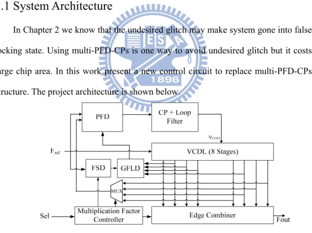
3.1 System Architecture
In Chapter 2 we know that the undesired glitch may make system gone into false locking state. Using multi-PFD-CPs is one way to avoid undesired glitch but it costs large chip area. In this work present a new control circuit to replace multi-PFD-CPs structure. The project architecture is shown below.
Fig. 3.1 Project system architecture of DLL based clock generator
At beginning PFD generates UP and DOWN signals according to phase difference between reference clock and feedback signal. CP charges or discharges LF by receiving UP and DOWN signals. Through control the voltage of LF we can
control total delay time of VCDL. When delay time locks at one time period of reference clock, edge combiner uses edges from VCDL to combine desired output frequency. The frequency multiplication factor of edge combiner is controlled by control circuit and control signal Sel. Control circuit includes multiplication factor controller, Feedback switching detector and modified lock controller. Feedback switching detector begins to work when feedback signal is switching. According to different situation feedback switching detector enforces CP charges or discharges to prevent undesired glitch. Glitch-free lock detector classifies system locking state into 3 states which are Upper, Active and Lower. Through this movement locking range can be extended. So the start-up circuit in multi-PFD-CPs structure is no need and saves more chip area. Using new control circuit to replace multi-PFD-CPs structure can reduce chip area by 37.8%. The following sections are set to show detail of each block.
3.2 Control Circuit
Control circuit contains 3 parts which are multiplication factor controller, feedback switching detector and glitch-free lock detector. Let us start at multiplication factor controller.
3.2.1 Multiplication Factor Controller
This block certainly controls the enable signal of edge combiner and feedback signal. Circuit input and output pattern is shown in Table 3.1. The relationship between enable signals will be described précised in section 3.7. Through the table and K-map we can know that:
1 2 2 3 8 2 3 7 1 3 2 6 1 2 3 4 2 3 2 3 5 3 1 ) ( , , , , Sel Sel Sel Sel S Sel Sel S Sel Sel Sel S Sel Sel Sel S Sel Sel S Sel S S S + ′ + = = + = + + = + = = = =
And the enable signal of feedback signal is easier to generate form Si signals.
) ( , ) ( , ) ( , 7 7 8 6 6 7 8 5 5 6 7 8 8 8 S E S S E S S S E S S S S E = = ′+ = ′+ + = ′+ + +
In this way, we can use the simplest logic gates to generate these control signals.
Table 3.1 Enable signal pattern
Input Output Sel3 Sel2 Sel1 S1 S2 S3 S4 S5 S6 S7 S8 E8 E7 E6 E5
0 0 0 0 0 0 1 0 0 0 0 1 0 0 0 0 0 1 0 0 0 1 0 0 0 1 1 0 0 0 0 1 0 0 0 0 0 0 1 0 0 0 0 1 0 0 1 1 0 1 0 1 0 1 0 1 1 0 0 0 1 0 0 1 1 1 1 1 0 0 0 0 0 0 1 1 0 1 1 1 1 1 1 1 0 0 0 0 1 0 1 1 0 1 1 1 1 1 1 1 0 0 1 0 0 1 1 1 1 1 1 1 1 1 1 1 1 0 0 0
3.2.2 Feedback switching detector
This block is design to avoid undesired glitch generates when feedback signal is switching. Detector through sensing rising edge and falling edge of signals to judges CP needs to be in charge or discharge condition. In order to sensing rising/falling edge we need rising edge trigger and falling edge trigger. These two blocks is shown in Fig. 3.2 and Fig. 3.3.When input signal has rising/falling edge, output generates a short pulse from 0 to 1. Use these two blocks and D-flip-flop we can acquire feedback switching detector which is shown in Fig. 3.4.
i
Fig3.2 Rising edge trigger
Fig. 3.3 Falling edge trigger
Fig. 3.4 Feedback switching detector
By detecting signal rising/falling edge we can judge delay time of VCDL shall be enlarged or shorted. If delay time should be shortened, set_upper sets to 1 and feeds into glitch-free lock detector. Then glitch-free lock detector forces CP charges LF and makes delay time smaller. Set_upper will be cleared at next rising edge of reference clock. Similarly, set_lower will be set for a while when delay time need to be enlarged. Through Fig. 3.5 we can understand how this block work easily. When enable signal falling means feedback signal is changing from VCDL’s 5th stage to other stage. No matter what stage is chosen to be feedback signal, delay time for each delay cell must be shortened. That is the control voltage must rise at that time, so
i
E
5
the set_upper signal sets to 1 to force CP charges LF. Similarly, at rising edge of , delay time for each delay cell must be enlarged. So set_lower is set to 1. At reference signal’s rising edge both set_upper and set_lower will be cleared. Based on this movement we can ignore undesired glitch problem.
5
E
Fig. 3.5 Feedback switching detector working example
3.2.3 Glitch-Free Lock Detector
Lock detector is used to generate PFD’s control signals. By using VCDL’s certain stages sample reference clock, lock detector can identify system locking status into 3 states. When upper sets to 1 means VCDL’s delay time is too long in comparison with reference clock’s time period. At the same time, PFD set UP signal to force CP charges so delay time will be shortened. On the contrary, lower sets to 1 means VCDL’s delay time is too short and PFD has to set DOWN signal. When VCDL’s delay time is closed to reference clock’s time period then active is set to 1. The UP/DOWN signals is determined by PFD at this state. There is only one of Upper, Lower and Active can be 1 at the same time. We can enlarge locking range through separate locking status into Upper, Active and Lower.
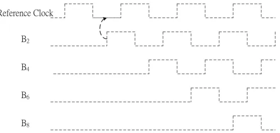
In [8], we can see the original type of lock controller and it’s shown in Fig 3.6. The output signals upper, active and lower are determined by the relationship between reference clock and Bi signals. Where Bi signals represents the ith stage of VCDL.
Using Bi signals to sample reference clock we can know the lock status. To explain more detailed, I use an example which feedback stage is 8th stage of VCDL. Lock detector uses 2nd, 4th and 6th stage of VCDL as D-flip-flops’ clock. And D-flip-flops’ inputs are reference clock. Let us see Fig. 3.7. If B2 signal samples at 0 which means the phase difference between reference clock and 2nd stage of VCDL is π ~ 2π and 8th stage is 4π ~ 8π. But the phase difference between feedback stage and reference clock should be 2π when system is locked. So at this moment delay should be shortened and output signal should set to 1. Similarly, in Fig. 3.8 we can see that when B2, B4 and B6 sample value are 1, 0 and 1 the phase difference should be 0.67π ~ π, 1.34π ~ 2π and 2π ~ 3π separately. And the phase difference between feedback stage and reference clock is 2.67π ~ 4π still far away from 2π. This locking status is upper too. In similarly way we can separate locking status into upper, active and lower. There is a summary in table 3.2.
Reference Clock B2
B4
B6
B8
Fig. 3.7 Example of lock detector when feedback stage is 8th stage of VCDL
Fig. 3.8 Example of lock detector when feedback stage is 8th stage of VCDL
Table 3.2 Lock detector work example when feedback stage is VCDL’s stage 8
Input Phase Difference Locking Status
Q1 Q2 Q3 Stage 2 Stage 4 Stage 6 Stage 8
0 X X π ~2π X X 4π ~8π Upper 1 0 1 π ~π 3 2 π π 2 ~ 3 4 2π ~3π π π 4 ~ 3 8 Upper 1 X 0 π π 3 2 ~ 3 1 X π ~2π π π 3 8 ~ 3 4 Active 1 1 1 π 3 1 < π 3 2 < < π π 3 4 < Lower
From Table 3.2 we can get 3 2 1 1 3 2 1 3
1Q ' ,Lower QQ Q andUpper Q ' QQ 'Q
Q
Active= = = +
Actually we can simplify it to
)' ( and )' ' ' ' ( , )' '
(Q2 Q6 Lower Q2 Q4 Q6 Upper Active Lower
Active= + = + + = +
In this way we can identify locking state into 3 states. In order to cooperates with feedback switching detector we need to make some changes. The structure after modified is shown in Fig. 3.9. The difference from original type is adding two input signals set_upper and set_lower. And we have to clear active and lower to 0 when set_upper is 1. Sets lower and clear active when set_lower is 1. After adding these two signal we can modified the formula to
)' ( and ) )' ' ' ' ( _ ( , )' ' _ _ ( 2 6 2 4 6 Lower Active Upper Q Q Q lower Set Lower Q Q lower Set upper Set Active + = + + + = + + + =
Fig. 3.9 Modified lock controller
When feedback stage changes to other stage, the clock of D-flip-flop may be changed. Clock inputs change to 2nd, 3rd and 4th stage when feedback stage is 5th and 6th stage. The clock input doesn’t change from feedback stage 8th to 7th. The operation
procedures are still the same, but locking range is changing with feedback stage. The operation range is summarized in table 3.3. According to table 3.3, we enlarge locking range at least to 2.5 Tref. In Chapter 2 we know the maximum traditional DLL’s locking range is only 1.5 Tref. Adding glitch-free lock detector in DLL based clock generator not only can enlarge locking range but also can fix undesired glitch problem.
Table 3.3 Each Status phase difference region Locking Status
Feedback stage
Lower Active Upper
8th <1.33π 1.33π~2.67π 2.67π~8π 7th <1.16π 1.16π~2.33π 2.33π~7π
6th <1.5π 1.5π~3π 3π~6π
5th <1.25π 1.25π~2.5π 2.5π~5π
3.3 PFD
The schematic of PFD is shown in Fig. 3.10. The difference from traditional PFD is adding three control signals into circuit. When Upper is 1, output Up keeps high and Down keeps low. On the contrary, output Up keeps low and Down keeps high when Lower is 1. PFD begins to work until active is 1. At rising edge of reference clock, Up is trigged to 1. Also, Down is trigged to 1 at rising edge of feedback signal. Up and Down are cleared to 0 when both Up and Down are 1. Arrived order of reference clock’s and feedback signal’s positive edge determined CP generates charge or discharge current to LF. When system is locked, the arrived time of two rising edge is the same. But Up and Down still trig to 1 for a short time, this movement can reduce dead zone of PFD.
REF FB Lower Upper Up Down Acti ve Act iv e Fig. 3.10 PFD’s schematic
3.4 CP and LF
In consideration of wide frequency range operation, the current mode CP is suitable for high speed operation. The CP schematic is shown in Fig. 3.11. Reference current is generated from the left part of circuit and use current mirror to mirror current to switch nodes. The switches are control by Up and Down signal. Node Vctrl is connecting to LF which is a simple capacitance.
3.5 Pulse Reshaper
In Chapter 2 we mention that CP current mismatch is unavoidable in wide range operation. The mismatch will cause statistic phase error and worse jitter performance when system locked. In this project, we use the pulse reshaper circuit in [10] to lessen current mismatch problem in CP.
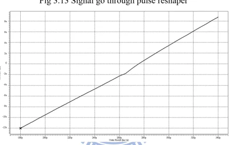
The schematic of pulse reshaper is shown in Fig. 3.12. The Up and Down signal is produced by PFD. Pulse resharper expand the difference between Up and Down by two low slew rate inverters. Fig 3.13 shows what happens when signal go through pulse reshaper. When Up and Down are the same, Rup and Rdn remain the same. But when difference between Up and Down is larger than Tm. The difference between Rup and Rdn become more obvious than between Up and Down. In other words, the gap between charge and discharge current become wider and PD gain becomes bigger. The slope of characteristic plot will be sharper by adding this block between PFD and CP. In Chapter 2 we know the sharper slope makes static phase error smaller. Fig 3.14 is the PD gain’s characteristic plot without pulse resharper and Fig 3.15 is PD gain’s characteristic plot with pulse resharper. This is obvious that Fig. 3.15 has sharper slope especially when phase difference approaches to 0.
Up Down Upb Downb Rdn Rup Tm Tm Tm (a) (b) (c) 0 = −VCDL
REF REF−VCDL<Tm REF−VCDL>Tm
Fig 3.13 Signal go through pulse reshaper
Fig. 3.14 Characteristic plot of PFD, CP and control circuit when feedback stage is 8
Fig. 3.15 Characteristic plot of PFD, CP, pulse reshaper and control circuit when feedback stage is 8
3.6 Delay Cell
Project uses current mode delay cell because of its lower power consumption. The schematic is shown in Fig. 3.16. There is a single-ended inverter which is composed of M2 and M3 series two transistor. The amount of delay is determined by the equivalent resistance of M1 and M4 which is controlled by its passing current. And the passing current is controlled by voltage Vctrl. M5 and M6 form another inverter which is served as output buffer. It also can compensate high frequency attenuation introduced by delay part. Because the number of VCDL’s stages can decide the number of multiplication factors and the delay range of VCDL. According our design goal we choose 8 stages delay line. In 2008 work total delay range of eight delay cells is shown in Fig. 3.17. And the delay range is 2.2ns to 5.2ns. The delay range is from 1.8ns to 4.2ns in 2009 work and is shown in Fig.3.18.
Fig 3.17 2008 work Delay Range of VCDL
3.7 Edge Combiner
In Chapter 2 we know that pulse toggled edge combiner provides the most number of multiplication factors with the same number of VCDL’s stages. So the pulse toggled method is suitable for a power management system. We adopt edge combiner structure in [7]. The edge combiner’s structure is shown in Fig. 3.19 and TPL circuit is shown in Fig 3.20. It can produce N multiplication factors where N is the number of VCDL’s delay element. And the multiplication factor can be N/2. In this project we have 8 stages delay element in VCDL so we can get 8 multiplication factors from 1/2 to 8/2. Compared to other types of pulse toggle edge combiner, this edge combiner has smaller parasitic capacitance. But the pulse width and the AND gates size need carefully design.
In the part of transition detectors, Ki signal generates a short negative pulse at the rising edge of Dei where Dei is the VCDL’s ith stage’s output. The Si is regarded as the enable signal of transition detector. Then the short negative pulses are combined by three stages of AND gate. In the end, one pulse make TPL toggled once. The multiplication factor is controlled by Si signal and feedback stage. For example, we set S1 ~ S8 to 1 and let feedback stage becomes 8th stage of VCDL when multiplication factor is 8/2. Once system locks, TPL will toggle every 1/8 Tref. Which means output frequency is 4 times Fref. The output of TPL is 50% duty cycle because of pulse toggle method edge combiner we adopt. Every multiplication factor has its own pattern of Si signal and specific feedback stage which are controlled by multiplication factor controller in control circuit. In the other hand, the pattern of Ki pulses is set to avoid Ki pulses overlap in three AND gates and thus maximize output frequency. According to [6], output frequency increases 15% when pattern of Ki pulse is as shown in Fig. 3.19. The K1 and K8, which generates by feedback stage, meet and
final stage of AND gate in the pattern. But K1 and K5 meet at 1st stage when feedback stage is 5. The meet between K1 and Ki which generates by feedback stage occur earlier make jitter performance worse than original pattern. Similarly, K1 and K7 meet at 2nd stage also make jitter performance worse when feedback stage is 7.
Fig. 3.19 Edge Combiner
In 2008 work, the size of AND gate and Ki pulse width is determined by trial and
error. We set symmetric AND gate’s size is
um um L W P 18 . 0 45 ) ( = um um L W N 18 . 0 10 ) ( = and
Ki pulse width 500ps make system work correctly. But the size of AND gates is so big that edge combiner consumes 21.572mW in pre-layout simulation, while whole system consumes 33.645mW in pre-layout simulation.
In the 2009 work we calculate more précised to reduce power consumption. As shown in Fig. 3.21, the design goal is enlarge output frequency range to 1.8GHz so the minimum time interval of Ki signal is 275ps. Because we don’t want Ki pulses overlapped with each other, we set the Ki’s rise time and fall time 50ps. And TPL need pulse consist at 0 for at least 100ps so TPL can work correctly. Under these constraints, we can derive final (6th) stage’s MOS’s size of edge combiner by current
formula ' ( )2 t gs V V L W k i= − and dt dV C I = . Where Vt =0.5, TPL’s input capacitance= 100fF and L=0.18um. We can obtain Wp=12.5um and Wn=2.5um. After simulation, we adjust Wp=16um and Wn=4.8um to conform the constraints.
Fig. 3.21 Simplified Edge Combiner
Then we use logical effort to calculate effort of every stage. F=GBH
There’re 3 NAND gates Î )3 3 4 ( = G There’s no branchÎB=1
We assume edge combiner’s input capacitance is equal to output capacitanceÎH=1
And the total stage of edge combiner is 6(3 NOT gates and 3 NAND gates)Î
The effort of each stage is 6 1.155 1
=
F
In the end, we round 1.155 to 1.2. According to the final stage’s MOS’s size and effort of each stage we can get other five stages’ MOS’s size. Each logic gates’ size are shown in Table 3.4. After redesign edge combiner, we reduce edge combiner’s power consumption from 21.572mW to 9.469mW and whole system’s power consumption form 33.645mW to 21.819mW. Also we enlarge maximum output frequency range to 1.8GHz.
Table 3.4 Logic gates’ size in edge combiner LP=LN=0.18um PMOS’s Width (um) NMOS’s Width (um) 1st NAND 5.5 1.7 2nd NOT 6.8 2.1 3rd NAND 8.4 2.6 4th NOT 10.4 3.2 5th NAND 12.8 4 6th NOT 16 4.8
Chapter 4
Simulation and Measurement Results
Previous chapter shows each sub-circuit’s pre-layout simulation results and this chapter shows the post layout simulation results. The measurement’s setup and results will be introduced later.
4.1 Locking range simulation
Simulation results of characteristic plots of PFD, CP, control circuit and pulse reshaper under different feedback stages are shown in Fig. 4.1 to Fig. 4.4. The plot is like expected divide into 3 parts. CP always discharges LF in Lower region. Similarly, CP always charges LF in Upper region. And current is decided by PFD in Active region. We have steeper slope when phase difference between reference clock and feedback signal approaches to 0. That is because pulse reshaper enlarges the gap between UP and DOWN signal when phase difference approaches to 0. Simulation results summarize in Table 4.1. The locking range is a little different from ideal condition. Active’s range is a little shrank but it doesn’t affect system work.
Fig. 4.1 Characteristic plot of PFD, CP, pulse reshaper and control circuit when feedback stage is 8
Fig. 4.2 Characteristic plot of PFD, CP, pulse reshaper and control circuit when feedback stage is 7
Fig. 4.3 Characteristic plot of PFD, CP, pulse reshaper and control circuit when feedback stage is 6
Fig. 4.4 Characteristic plot of PFD, CP, pulse reshaper and control circuit when feedback stage is 5
Table 4.1 Summary of locking range Locking Status
Feedback stage
Lower Active Upper
8th <1.38π 1.38π~2.62π 2.62π~8π 7th <1.21π 1.21π~2.29π 2.29π~7π 6th <1.61π 1.61π~2.94π 2.94π~6π 5th <1.32π 1.32π~2.45π 2.45π~5π
4.2 Whole system simulation
4.2.1 2008 Work Post-Layout Simulation
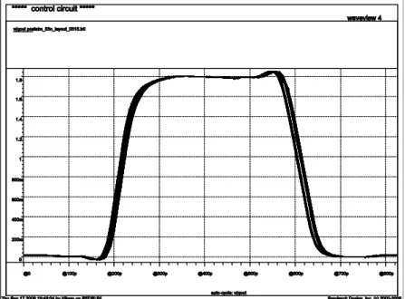
The post-layout simulation of different input reference clocks is shown from Fig. 4.5 to Fig. 4.8. We can see that at different input reference clocks system jitter performance is all under 20ps. The summary is shown in table 4.2.
Fig. 4.6 Eye diagram of input clock is 300MHz and multiplication factor is 4
Table 4.2 Performance of 2008 work post layout simulation
PostSim Process 0.18um Operating voltage 1.8v
Operating frequency range 200MHz~400MHz Output frequency range 100MHz~1.6GHz
Peak-to-peak jitter
17.255ps @ 800MHz 8.949ps @ 1.2GHz
[email protected] Power dissipation [email protected] Active area(Without PAD) 182um*214um
= 0.0389(mm*mm) Layout area(With PAD) 0.688mm*0.688mm =0.473(mm*mm)
4.2.2 2009 Work Post-Layout Simulation
In this version, we fix the issues found in previous measurement. We will show that system is stable at every multiplication factors. The other change is output frequency range. We show system jitter performance at different reference clock in this section. The comparison and performance table is shown in the end of this section. We do reduce power consumption by 16mW from previous measurement.
The following 8 pictures is Eye diagram when reference clock is 450MHz under different multiplication factors. And the jitter performance is summarized in table 4.3. The results show jitter performance is all under 20ps after fix the mismatch. Fig. 4.16 shows VCTRL’s change at different feedback stage. From Fig. 4.16 we can know system’s lock time is smaller than 200ps.
Fig. 4.8 Eye diagram: Reference clock is 450MHz and multiplication factor is 4
Fig. 4.10 Eye diagram: Reference clock is 450MHz and multiplication factor is 3
Fig. 4.12 Eye diagram: Reference clock is 450MHz and multiplication factor is 2
Fig. 4.14 Eye diagram: Reference clock is 450MHz and multiplication factor is 1
Feedback stage = 8 Feedback stage = 7 Feedback stage = 6 Feedback stage = 5
Fig. 4.16 VCTRL at each feedback stage
Different reference clocks
The following pictures are Eye diagram under different reference clock. The results demonstrate system is work at input frequency range from 250MHz to 450MHz and output frequency range is from 125MHz to 1.8GHz.
Fig. 4.18 Eye diagram: Reference clock is 350MHz and multiplication factor is 4
Table 4.3 Performance of 2008 work post layout simulation 2009 work (Post-SIM) input frequency 250M~450M output frequency 125M~1.8G Power 21.819mW Multiplier factor 1/2~8/2 RMS jitter [email protected] P-P Jitter 8.805ps @1.8GHz P-P Jitter (under different MF, test by maximum reference signal) 8.805ps @1.8GHz 12.707ps @1.575GHz 7.598ps @1.35GHz 16.937ps @ 1.125GHz 5.17ps @ 900MHz 8.882ps @ 675MHz 2.923ps @ 450MHz 5.634ps @ 225MHz Chip Area 0.698*0.643mm2
4.3 Measurement setup
Both 2008 and 2009 work are fabricated in TSMC 0.18um CMOS technology. Die photos are shown in Fig. 4.20 and Fig. 4.21 separately. The PCB is shown in Fig.4.22 and Fig. 4.23. The 2008 work’s measurement environment is shown in Fig. 4.24. We use clock generator HP-8133A generates reference clock to chip and use oscilloscopes DSA-70804 to observe output signal. The 2009 work’s measurement environment is shown in Fig. 4.25. The only difference is that we use signal generator, Rohde & Schwarz SML03, to replace HP 8133A.
Fig. 4.20 2008 Work Die Photo
Fig. 4.21 2009 Work Die Photo
Fig. 4.23 2009 Work Prototype PCB VDD(1.8v) REF Q Control Signals (On PCB) Control LABORATORY GPC-3060C HP -8133A Tektronix DSA-70804
Fig. 4.24 2008 Work Measurement environment
4.4 Measurement Results
4.4.1 Measurement results of 2008 Work
The Eye diagrams of 2008 work are shown in Fig. 4.26 to Fig. 4.29. The measurement results and comparison with post-layout simulation is summarized in table 4.4.
Fig. 4.26 Eye [email protected], P-P Jitter : 23.316ps, Population : 13767
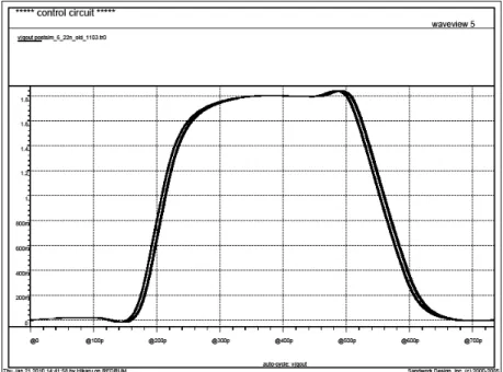
Fig. 4.28 Eye [email protected], P-P Jitter : 9.065ps, Population : 12804
Table 4.4 Performance Summary of 2008 work
Post-layout Simulation Measurement
Input frequency range 200MHz~400MHz 200MHz~400MHz
Output frequency range 100MHz~1.6GHz 100MHz~1.6GHz
P-P Jitter (under different MF, test by 400MHz reference signal) 7.926ps @1.6GHz 19.398ps @1.4GHz 42.567ps @1.2GHZ 58.524ps @ 1GHz 8.371ps @ 800MHz 42.148ps @ 600MHz 0.358ps @ 400MHz 0.433ps @ 200MHz 24.316ps @1.6GHz 45.11ps @1.4GHz 66.643ps @1.2GHZ N/A @ 1GHz 24.168ps @ 800MHz N/A @ 600MHz 9.065ps @ 400MHz 28.929ps @ 200MHz Power consumption 34.418mW @ 1.6G [email protected]
After measurement we find out some issues in 2008 Work. One of the issues is jitter performance is quite different from post-layout simulation. Jitter goes worse when feedback stage is not 8. The reason is mismatch of MUXs in front of PFD. The mismatch causes different delay time between reference clock and feedback signal. So system will not lock at reference clock’s one time period and jitter performance is bad. The other issue is too much power is spending on edge combiner. So at 2009 work we redesign edge combiner to reduce power consumption. The detail is mentioned in Chapter 3.7. These issues are fixed in 2009 work and the measurement results are shown in following section.
4.4.2 Measurement results of 2009 Work
The measurement results are shown below. From Fig. 4.30 to Fig 4.33 are the Eye diagrams and histograms. We set supply voltage is 2.5V when measuring. The performance summary is shown in Table 4.5 and the power consumption at each
output frequency is shown in Table 4.6. The power consumption is much higher in measurement because the supply voltage is 2.5V instead 1.8V. Besides, compared to Post-layout simulation, measurement results present little higher jitter performance when output frequency goes higher. The first reason is the reference clock is ideal in simulation, but it’s not in measurement. The second reason is because there are the delay mismatches between delay cells. Although the total delay of VCDL is equal to TREF. Each delay of delay cells is different. For example, we assume the TREF is 8ns and the number of delay cells is 8. Delay of each delay cell is 1ns ideally. But if there are mismatches between delay cells, the delay may be 1.05ns, 1.05ns, 1.05ns, 1.05ns, 0.95ns, 0.95ns, 0.95ns and 0.95ns. Total delay remains 8ns, but the mismatch makes jitter bigger. When multiplication is 0.5 or 1, output clock is transition at the same delay cell. So at these two multiplication factors, jitter performance is better than at others multiplication factors. The histograms also can explain the effect of delay mismatch. In Fig. 4.31, there are two groups of data. Contrary, in Fig. 4.32, there is only one group of data.
Fig. 4.31 Eye [email protected], RMS Jitter: 2.628ps, P-P Jitter: 13.925ps
Fig. 4.32 Eye [email protected], RMS Jitter: 0.831ps, P-P Jitter: 6.096ps
Table 4.5 2009 work performance at supply voltage = 2.5V 2009 work (Post-Simulation) 2009 work (Measurement) input frequency 250M~450M 250M~450M output frequency 125M~1.8G 125M~1.8G Power 21.819mW 45.973mW Multiplier factor 1/2~8/2 1/2~8/2 RMS jitter [email protected] [email protected] P-P Jitter (under different MF, test by maximum reference signal) 8.805ps @1.8GHz 12.707ps @1.575GHz 7.598ps @1.35GHz 16.937ps @ 1.125GHz 5.17ps @ 900MHz 8.882ps @ 675MHz 2.923ps @ 450MHz 5.634ps @ 225MHz 26.881ps @1.8GHz 36.766ps @1.575GHz 26.888ps @1.35GHz 38.163ps @ 1.125GHz 13.925ps @ 900MHz 35.118ps @ 675MHz 8.031ps @ 450MHz 9.961ps @ 225MHz Chip Area 0.698*0.643mm2 0.698*0.643mm2
Table 4.6 Power consumption at each output frequency Power Consumption
( Multiplication factor = 4, Supply Voltage = 2.5V, Under different input frequency )
45.973mW @ 1.8G 41.723mW @ 1.6G 37.895mW @ 1.4G 33.335mW @ 1.2G 28.725mW @ 1.0G
4.5 Performance Summary
Table 4.7 is the performance comparison between 2009 and 2008 work. After fix the mismatch in front of PFD, we maintain jitter performance under every multiplication factor. Also, the output frequency is enlarged to 1.8GHz at 2009 work.
Table 4.7 Comparison between 2008 and 2009 work
2008 Work (Measurement) 2009 work (Measurement) input frequency 200M~400M 250M~450M output frequency 100M~1.6G 125M~1.8G Power [email protected] [email protected] Multiplier factor 1/2~8/2 1/2~8/2 RMS jitter 7.759ps @ 1.6GHz [email protected] P-P Jitter 24.316ps @1.6GHz 26.881ps @1.8GHz P-P Jitter (under different MF, test by maximum reference signal) 24.316ps @1.6GHz 45.11ps @1.4GHz 66.643ps @1.2GHZ N/A @ 1GHz 24.168ps @ 800MHz N/A @ 600MHz 9.065ps @ 400MHz 28.929ps @ 200MHz 30.398ps @1.6GHz 51.636ps @1.4GHz 20.905ps @1.2GHZ 56.293ps@ 1GHz 10.438ps @ 800MHz 45.03ps@ 600MHz 6.94ps @ 400MHz 8.342ps @ 200MHz Chip Area 0.698*0.698mm2 0.698*0.643mm2
Table 4.8 shows the comparison between this work and other reference papers. This work has 8 multiplication factor is the most in reference paper. Compared to [7], which can generate as many multiplication factors as our work, our work has much lower power consumption.
Table 4.8 Compare with reference papers
2008 Work
measurement
2009 Work
measurement [9] [8] [7] [23]
process 0.18um 0.18um 0.35um 0.18um 0.35um 0.13um
Supply 1.8V 1.8V 3.3V 1.8V 3.3V 1.2V input frequency 200M~ 400M 250M~ 450M 240M~ 275M 275M~ 800M 240M~ 450M 250M~ 500M output frequency 100M~ 1.6G 125M~ 1.8G 120M~ 1.1G 137.5M~ 3.2G 120M~ 1.8G 125M~ 2G Power 37.8mW @1.6GHz 45.973mW @1.8GHz 42.9mW 36.7mW @1.7GH z 86.6mW @1.6GHz 21mW @2GHz Multiplier factor 1/2~8/2 1/2~8/2 0.5, 1 , 2, 4 0.5, 1 , 2, 4 1/2~8/2 0.5, 1 , 2, 4 RMS jitter 7.759ps @ 1.6G 8.395ps @ 1.8G 2ps@1G 2.64ps 1.8ps@ 1.3G 3.16ps @1G P-P Jitter 23.316ps @ 1.6G 26.881ps @ 1.8G ±7.28ps @1G 16.8ps @1.7G ±6.6ps @1.3G 19ps @1G Active area(mm^2) 0.039 0.045 0.07 0.043 0.07 0.019 Year JSSC .2002 ASSCC .2007 JSSC .2006 TCSII .2009
Chapter 5
Conclusion and Future Works
5.1 Conclusion
In the thesis a wide frequency range, glitch free, and Low-Power DLL based clock generator is implemented. In Chapter 2 we discuss design challenges of designing DLL based clock generator such as locking issue, wide range locking issue and multiplication factor issue. Using feedback switching detector to replace multi-PFD-CPs structure can lower active area by 25%. The locking range is extended to 2.5Tref by adding lock detector into system. Eventually we get 8 multiplication factors by adopting edge combiner in [7] and the output frequency range is from 125MHz to 1.8GHz.
2008 work is implemented in TSMC 0.18um 1P6M CMOS technology. Measurement results show system is function work. In 2008 work, the jitter is 24.316ps and power consumption is 37.8mW when output frequency is 1.6GHz. After fixing MUX mismatch problem, we maintain jitter performance under every multiplication factor. In 2009 work, the RMS jitter is 8.395ps and power consumption is 45.973mW when output frequency is 1.8GHz. The revise makes this DLL based clock generator more suitable for a power management system.
5.2 Future Work
In order to solve multi-tone problem, observed in measurement, we need redesign delay cells to fix the delay mismatch. Besides, the more multiplication factors can make power management system more efficient. We can increase the number of VCDL’s delay cells since we enlarge the locking range. In this way, we can get more multiplication factors and thus make power management system more efficient.
Reference List
[1] H. Chiueh, et al., "A dynamic thermal management circuit for system-on-chip designs," in Electronics, Circuits and Systems, 2001. ICECS 2001. The 8th IEEE International Conference on, 2001, pp. 577-580 vol.2.
[2] Intel, "Enhanced Intel® SpeedStep® Technology for the Intel® Pentium® M Processor," 2004.
[3] B.-H. Lu, "A 100MHz-1.6GHz DLL-Based Clock Generator with Switching Glitch and Static Phase Error Reduction Function," Master, Communication Engineering, National Chiao Tung University, Hsinchu, Taiwan, 2009.
[4] G. Chien, "Low-noise local oscillator design techniques using a DLL-based frequency multiplier for wireless application,," University of California, Berkeley, PhD Thesis, 2000.
[5] D. J. Foley and M. P. Flynn, "CMOS DLL-based 2-V 3.2-ps jitter 1-GHz clock synthesizer and temperature-compensated tunable oscillator," Solid-State Circuits, IEEE Journal of, vol. 36, pp. 417-423, 2001.
[6] L. Chih-Hsing and C. Ching-Te, "A 2.24GHz Wide Range Low Jitter DLL-Based Frequency Multiplier using PMOS Active Load for Communication Applications," in Circuits and Systems, 2007. ISCAS 2007. IEEE International Symposium on, 2007, pp. 3888-3891.
[7] K. Jin-Han, et al., "A 120-MHz-1.8-GHz CMOS DLL-Based Clock Generator for Dynamic Frequency Scaling," Solid-State Circuits, IEEE Journal of, vol. 41, pp. 2077-2082, 2006.
[8] C. Kyunghoon, et al., "An anti-harmonic, programmable DLL-based frequency multiplier for dynamic frequency scaling," in Solid-State Circuits Conference, 2007. ASSCC '07. IEEE Asian, 2007, pp. 276-279.
[9] K. Chulwoo, et al., "A low-power small-area ±7.28-ps-jitter 1-GHz DLL-based clock generator," Solid-State Circuits, IEEE Journal of, vol. 37, pp. 1414-1420, 2002.
[10] P. T. Torkzadeh, A.; Atarodi, M., "A Wide Tuning Range, 1GHz-2.5GHz DLL-Based Fractional Frequency Synthesizer," ISCAS, vol. 5, pp. 5031 - 5034, 2005.
[11] J. G. Maneatis, "Low-jitter process-independent DLL and PLL based on self-biased techniques," Solid-State Circuits, IEEE Journal of, vol. 31, pp. 1723-1732, 1996.
[12] G. Chien and P. R. Gray, "A 900 MHz local oscillator using a DLL-based frequency multiplier technique for PCS applications," in Solid-State Circuits Conference, 2000. Digest of Technical Papers. ISSCC. 2000 IEEE International, 2000, pp. 202-203, 458.
[13] R. Farjad-Rad, et al., "A low-power multiplying DLL for low-jitter multigigahertz clock generation in highly integrated digital chips," Solid-State Circuits, IEEE Journal of, vol. 37, pp. 1804-1812, 2002.
[14] C. Hsiang-Hui, et al., "A wide-range delay-locked loop with a fixed latency of one clock cycle," Solid-State Circuits, IEEE Journal of, vol. 37, pp. 1021-1027, 2002.
[15] M. J. E. Lee, et al., "Jitter transfer characteristics of delay-locked loops - theories and design techniques," Solid-State Circuits, IEEE Journal of, vol. 38, pp. 614-621, 2003.
[16] C. Kuo-Hsing, et al., "A 2.2 GHz programmable DLL-based frequency multiplier for SOC applications," in Advanced System Integrated Circuits 2004. Proceedings of 2004 IEEE Asia-Pacific Conference on, 2004, pp. 72-75.
![[2016-Fall] WNFA lab3 - JJY](data:image/gif;base64,R0lGODlhAQABAIAAAP///wAAACH5BAEAAAAALAAAAAABAAEAAAICRAEAOw==)