國
立 交 通 大 學
電子工程學系 電子研究所碩士班
碩 士 論 文
氟摻雜對二氧化鉿堆疊式閘極 P 型金氧半場
效電晶體其可靠性的影響
Effect of Fluorine Incorporation on the Reliability
Issue of pMOSFETs with HfO2/SiON Gate Stack
研 究 生:王信智
指導教授:葉清發 博士
羅正忠 博士
氟摻雜對二氧化鉿堆疊式閘極 P 型金氧半場
效電晶體其可靠性的影響
Effect of Fluorine Incorporation on the Reliability
Issue of pMOSFETs with HfO2/SiON Gate Stack
研 究 生:王信智 Postgraduate:Hsin Chih Wang
指導教授:葉清發 博士 Advisor:Dr. Ching-Fa Yeh
羅正忠 博士 Dr. Jen-ChungLou
國 立 交 通 大 學
電子工程學系 電子研究所碩士班
碩 士 論 文
A Thesis
Submitted to Department of Electronics Engineering & Institute of Electronics Engineering and Computer Science
National Chiao-Tung University in partial Fulfillment of the Requirements
for the Degree of Master of Science in
Electronics Engineering June 2007
Hsinchu, Taiwan, Republic of China
-I-
氟摻雜對二氧化鉿堆疊式閘極 P 型金氧半場
效電晶體其可靠性的影響
研究生:王信智
指導教授: 葉清發博士
羅正忠博士
國立交通大學 電子工程學系 電子研究所碩士班 摘要 根據半導體積體電路的微縮定理,極薄的二氧化矽介電質層(1 至 1.5 奈米) 將遭遇量子穿遂效應的問題而導致極大的洩電流,導致元件可靠度上的問題。近 年來使用高介電質材料來取代傳統以二氧化矽當介電質層已廣泛被研究。相較於 二氧化矽,由於在相同的等效厚度之下高介電質物質有較厚的實際厚度,因此可 以抵擋因量子的穿遂效應而導致的大量漏電。然後,以高介電質材料當閘極介電 質層卻遭遇到其它的問題。例如:相對於二氧化矽操作在相同電壓下,高介電質材 料有較高的界面狀態產生及較多的電荷捕捉,這對於元件操作時臨限電壓的漂移 有較嚴重的影響。 在 P 型金氧半場效電晶體中,負偏壓溫度不穩定效應是主要的問題。我們於-II- 閘極介電質沈積前,以離子佈值的方式植入氟摻雜,使氟原子在後續的高溫摻雜 活化的過程中,使其擴散至通道和閘極介電質層。利用氟的摻入,我們深入的探討 氟對二氧化鉿/氮氧化矽閘極之 P 型金氧半場效電晶體對於負偏壓溫度不穩定效 應的影響。我們發現,摻雜氟對於元件的基本特性,沒有顯著的降級。但對於固定 電壓應力(CVS)以及負偏壓-溫度應力(NBTS)量測時,含氟摻雜的元件有較低的界 面狀態產生,和較少的電荷捕捉,對於元件的可靠度和穩定性有明顯的改善,因此 改善了以高介電質材料為閘極介電極層的穩定性和可靠性。
-III-
Effect of Fluorine Incorporation on the Reliab ility
Issue of pMOSFETs with HfO2/SiON Gate Stack
Student : Hsin Chih Wang Advisor : Dr. Chin-Fa Yeh
Dr. Jen-ChungLou
Department of Electronics Engineering & Institute of Electronics
National Chiao Tung University
Abstract
According scaling rule, ultra-thin oxide(about 1~1.5nm) will undergo tunneling effect and then cause gate leakage current , which is the issue of the reliability . Recently , high dielectric constant materials are used to replace SiO2 has widely
studied. Compare with SiO2 at the same equivalent oxide thickness (EOT) , high
dielectric constant materials have thicker physical thickness which can resist tunneling effect , and then avoid leakage current . However , using high dielectric constant materials as gate dielectric experience other problems . For example , high dielectric constant materials have higher interfacial states and charge traps , these will cause more serious threshold voltage shift when working device as the same voltage compare with SiO2 .
-IV-
incorporate F before gate dielectric deposition via channel implantation technique, which was subsequently diffused into the gate stack during annealing process . By fluorine incorporation , we discuss the effects of negative bias temperature instability (NBTI) of F incorporated in pMOSFETs with HfO2/SiON stack in depth . We found
that F incorporated improves the fundamental electrical properties of the fabricated transistors . In addition , under constant voltage stress (CVS) and negative bias temperature stress (NBTS) , we found that lower generation rate of interface states and charge trapping are observed for device with F incorporation , thus enhances the reliability and the stability of high-k devices.
-V-
致謝
在二年的努力下,此篇碩士論文才能順利完成,有相當多的人要感
謝。首先,要感謝我的指導教授葉清發博士和羅正忠博士,在二年的指
導讓我學習到很多做研究的方法以及為人處世的方法。其次要感謝實
驗室的學長們,打從心裡感謝永裕學長在口試前給的建議、伯翰學長
教導量測的方法以及做實驗的方法、柏村學長為實驗室爭取資源。再
者,感謝帶我玩遍新竹的慧敏、世璋學長、湯尼伯、很堅持己見的德
安、愛走天漄的智仁、生氣來很嚇人的正凱、打電動不耐煩的大峰、
猶豫不決的小天、疼老婆的建宏,以及學弟幸福、佳樺、土豆、鄭元
愷、洪晨修、簡嘉宏。最後要感謝我的爸爸王英富、媽媽程錦碧,這
二年來的支持。有很多話要說,千言萬語都帶表不了我的謝意。總之,
謝謝各位我認識的人。
-VI-
Contents
Abstract (Chinese)………...I
Abstract (English) ………...II
Acknowledgement……….V
Contents………....VI
Table Captions………..….VIII
Figure Captions……….. ……..…...IX
Chapter 1 Introduction
……….
1
1-1 Backgrounds and Motivation……….……...1
1-2 Organization of the Thesis………3
Chapter 2 Electrical Characteristics of Fluorine
Incorporation on pMOSFETs with
HfO
2/SiON Gate Stack……….
5
2-1
Introduction………..………...5
2-2
Experiment………..6
2-2.1
Experimental Procedure………..………..6
-VII-
2-3. Result and Discussion………...………..9
2-2.3
Electrical characteristics of pMOSFETs with and without fluorineincorporation
...9
2-2.4
Conduction mechanism of pMOSFETs with HfO2/SiON GateStack
………...11
2-4. Summary……….………..15
Chapter 3 Impact of Fluorine Incorporation on the
Reliability of pMOSFETs with HfO
2/SiON
Gate Stack
………
35
3-1 Introduction……..………..………...35
3-2 The Models of NBTI and the Mechanism of Fluorine Incorporation
Alleviate NBTI Degradation………...…………...36
3-2.1
The Models of NBTI……….………… 36
3-2.2
The mechanism of Fluorine Incorporation Alleviate NBTI Degradation……….………..40
3-3 Measurements Setup………..……...41
3-4 The Reliability of Control and Fluorine-Incorporated
Devices………...42
-VIII-
3-4.2
NBTI of Control and Fluorine-Incorporated Devices………...44
3-5 Summary………...45
Chapter 4 Conclusion and Future Work
………...62
4-1
Conclusion……….………...62
4-2
Future Work………...………...63
Reference
……...……….64
Table Captions
Table 1-1
2005 International Technology Roadmap for Semiconductors. The color shade means the solution known and unknown for physics limit.-IX-
Figure Captions
Fig. 2-1 Fluorine incorporation via channel implantation.
Fig. 2-2 The process flow of pMOSFETs with HfO
2/SiON gate stack.
Fig. 2-3 Schematic cross section of pMOSFETs with HfO
2/SiON gate
stack.
Fig. 2-4 Basic experimental setup of charging pumping measurement.
Fig. 2-5 Configuration for (a)gate-to-channel, and (b)gate-to-substrate
capacitance measurement.
Fig. 2-6 C-V curves for pMOSFETs.
Fig. 2-7 Id-Vg & Gm-Vg characteristics of devices with and without
fluorine incorporation at V
D=0.1V.
Fig 2-8 I
d-V
dcharacteristics for devices with and without fluorine
incorporation.
Fig. 2-9 Compared Id
linearwith channel length for device with and
without fluorine.
Fig.2-10 Compared Gm
maxwith different channel length for device with
and without fluorine.
-X-
for device with and without fluorine.
Fig. 2-12 Compared threshold voltage with channel length for device
with and without fluorine.
Fig. 2-13 Compared Gm
maxwith channel width for device with and
without fluorine.
Fig. 2-14 Compared threshold voltage with channel width for device
with and without fluorine.
Fig. 2-15 Compared Gm
maxwith area for device with and without f
fluorine.
Fig. 2-16 Compared threshold voltage with area for device with and
without fluorine.
Fig. 2-17 Charge pumping current for device with and without fluorine
incorporation
Fig. 2-18 Compared hole mobility with effective field for device with
and without fluorine.
Fig. 2-19 Gate leakage current versus gate bias for fresh p-channel
devices at room temperature.
Fig. 2-20 Carrier separation under inversion region (a) control sample,
and (b)with F sample.
-XI-
Fig. 2-21 Carrier separation under accumulation region (a) control
sample, and (b)with F sample.
Fig. 2-22 p+-gated pMOSFET with HfO2/SiON gate stack under
inversion region (a) band diagrams, and (b) Schematic
illustration of carrier separation experiment.
Fig. 2-23 p
+-gated pMOSFET with HfO
2/SiON gate stack under
accumulation region (a)band diagrams , and (b)Schematic
illustration of carrier separation experiment.
Fig. 2-24 Gate leakage current versus gate bias without fluorine
incorporation for fresh p-channel devices at different
temperature.
Fig. 2-25 Gate leakage current versus gate bias with fluorine
incorporation for fresh p-channel devices at different
temperature.
Fig. 2-26 conduction mechanism for source/drain current fitting under
inversion region (a) without fluorine sample (b) with fluorine
sample.
Fig. 2-27 conduction mechanism for substrate current fitting under
inversion region (a)without fluorine sample (b) with fluorine
-XII-
sample.
Fig. 3-1 SIMS profile of F and B atoms for as-implanted and after
annealing with and without F implantation. (Ref[])
Fig. 3-2 Fluorine diffuses into HfO
2/SiON stack and forms stronger
Si-F bonds compared to Si-H bonds , and reduce charging
trapping by bonding to Hf dangling bond result in annihilation
of oxygen vacancies.
Fig. 3-3 Basic measurement method for (a) CVS (constant voltage
stress), and (b)NBTS (negative bias temperature stress).
Fig . 3-4 I
d-V
gcharacteristics for p
+-gated pMOSFETs before and after
stress1000 at 25 ℃ (a) control sample, and (b) fluorine
sample.
Fig. 3-5 Threshold voltage shift as a function of stress time, stressed at
25℃, Vg= -2~ -3V in linear scale (a) control sample ,and (b)
fluorine sample.
Fig. 3-6 Threshold voltage shift as a function of stress time, stressed at
25℃, Vg= -2~ -3V in linear scale (a) control sample ,and (b)
fluorine sample.
-XIII-
time, stress at 25℃, V
g=-3V.
Fig. 3-8 Interface trap density shift , and total trap density increase as a
function of stress time (a)control sample ,and (b) fluorine
sample.
Fig 3-9 interface state increase and total trap density increase versus
stressing time for control and fluorine-incorporated sample,
stressed at 25℃, Vg=-3V.
Fig. 3-10 I
d-V
gcharacteristics for p
+-gated pMOSFETs before and after
stress1000 at 125℃ (a) control sample (b) fluorine sample
Fig. 3-11 Interface trap density shift as function of stress time under
BTS at different stress temperature, Vg=-3V , with fluorine
sample
Fig. 3-12 Threshold voltage shift as a function of stress time under BTS
at different stress temperature , V
g=-3V in linear scale (a)
control sample, and (b) fluorine sample.
Fig. 3-13 Threshold voltage shift as a function of stress time under BTS
at different stress temperature , V
g=-3V in logarithm scale (a)
control sample, and (b) fluorine sample.
-XIV-
time under BTS at 25℃ and 125℃ , V
g=-3V
Fig. 3-15 Total trap density increase as a function of stress time under
BTS at different stress temperature , V
g=-3V (a) control
sample , and (b) fluorine sample
Fig. 3-16 Total trap density increase as a function of stress time under
BTS at different stress temperature , V
g=-3V for device with
-1-
Chapter 1
Introduction
1-1 Backgrounds and Motivation
With the developing of the IC (integrated circuit) technology , the rapid shrinking
of the metal oxide field effect transistors (MOSFETs) has confronted the channel length and gate dielectric thickness to also decrease rapidly . The research point out that when conventional SiO2 gate insulator scales to at least 1.0nm~1.5nm , large gate
leakage current tunnels from this ultra-thin oxide and then causes the reliability issues . To suppress above , high dielectric constant (high-k) materials has widely investigated [1]. The main reason of using high dielectric constant materials to replace conventional SiO2 is : under the same equivalent oxide thickness (EOT) , high
dielectric constant materials have thicker physical thickness which can avoid gate leakage current generating .Therefore , we will require high-k gate dielectrics to seek the specification in ITRS (Table 1-1) [2] in terms of sufficiently low gate leakage combined with ultra-thin equivalent oxide thickness (<1nm)
There are several high-k dielectrics have studied in recent . Hafnium oxide (HfO2)
is considered as one of the most promising candidates , since its thermal stability in contact with silicon (47.6Kcal/mole at 727℃) compared to TiO2 and Ta2O5 , high
-2-
5.6eV with band offsets to silicon >1.5eV , appropriate barrier high for both electrons and holes (> 1eV) , and compatible with poly-silicon . However , there are still a number of pending issues when high-k dielectrics are liable applied in future technology nodes , including high density of traps in the bulk dielectric and interfacial layer which will cause mobility degradation and threshold voltage instability . Therefore , how to improve bulk traps and interfacial traps is our goal . Except this , the reliability of high-k dielectrics is need to be understand in order to introduce to CMOS technology .
Abundant literatures have been published about the methods of incorporating nitrogen [3-4] or Si [5-6] into Hf-based films/stack in order to improve the film quality. Recently, some literatures have also incorporated fluorine into different high-k gate dielectrics by different ways [7-8-9]. The results reveal the breakthrough of device reliability and performance are indeed improved . In this thesis, fluorine are incorporated into HfO2/SiON gate stack via channel implantation before gate
dielectric growths, and its impact on the pMOSFETs are studied . It was clearly seen that the degradation is improved in the F-incorporated sample. More importantly , we also found less shift of threshold voltage under CVS (constant voltage stress ) and NBTS (negative bias temperature stress ) in this sample. We believe it has the potential to be an industrial standard if ALCVD HfO2 is the final selection of future
-3- dielectric of the ULSI industry .
1-2 Organization of This Thesis
In this chapter, we introduce the reason of the high-k dielectrics on CMOS technology and systematic discuss the effect of fluorine incorporating on pMOSFETs with HfO2/SiON gate stack.
In chapter 2 , we describe the process flow for fabricating pMOSFETS test devices with HfO2/SiON gate stack . We will show some basic electrical characteristics with
and without fluorine incorporation, split C-V to obtain mobility , charging pumping to verify the amount of interface states and carrier separation to gain leakage current mechanisms .
In chapter 3, we discuss the reliability issues such as constant voltage stress (CVS) , negative bias temperature stress (NBTS) of the devices with and without fluorine incorporation .
In chapter 4 , we conclude the result and important discovery in this research . Some suggestion for future work about fluorine incorporating is given .
-4-
Table 1-1 2005 ITRS roadmap
Manufacturable solutions, and are being opitimized.
Manufacturable solutions are known.
Manufacturable solutions are not known.
Years of Production 2005 2006 2007 2008 2009 2010 2011 EOT (Physical ) for
High –performance(nm) 1.2 1.1 1.1 1.0 0.9 0.65 0.5 Electrical thickness adjustment for gate
depletion and inversion layer effects (nm)
0.73 0.74 0.74 0.7 0.7 0.27 0.25
Nominal gate leakage current density
-5-
Chapter 2
Electrical Characteristics of Fluorine
Incorporation on pMOSFETs with HfO
2/SiON
Gate Stack
2-1 Introduction
Fluorine incorporation in silicon dioxide gate dielectrics has widely studied in 1980s. The research pointed out that fabrication of transistors with fluorine-enriched oxide will not show degradation as long as the concentration is sufficiently low. The research also found fluorine have caused an improvement in interfacial properties [10].
In high-k dielectrics we faced high defect density in the bulk of high-k gate
dielectric and interfacial state in the gate stack structure are major reasons for Vth
instability and mobility degradation [11]. Recently, the research of fluorine incorporation into CMOS has studied in high-k gate dielectrics with different methods , such as channel implantation [9] , gate implantation [7] and UV-F2 [8].
They indicated that fluorine piles up in the bulk of dielectric, but excessive amount of fluorine ions are present in the dielectric will increase the leakage current [12]. In this chapter, we compared with electrical characteristics for pMOSFETs with and
-6-
without fluorine incorporation, which was implemented by channel implantation. We found the 5E13cm-2 sample doesn’t cased severe damage while channel implantation compared with the non-fluorine sample. On the contrary, it make the electrical characteristics better like mobility enhancement and driving current increase without serious leakage current.
2-2 Experiment
2-2.1 Experimental Procedure
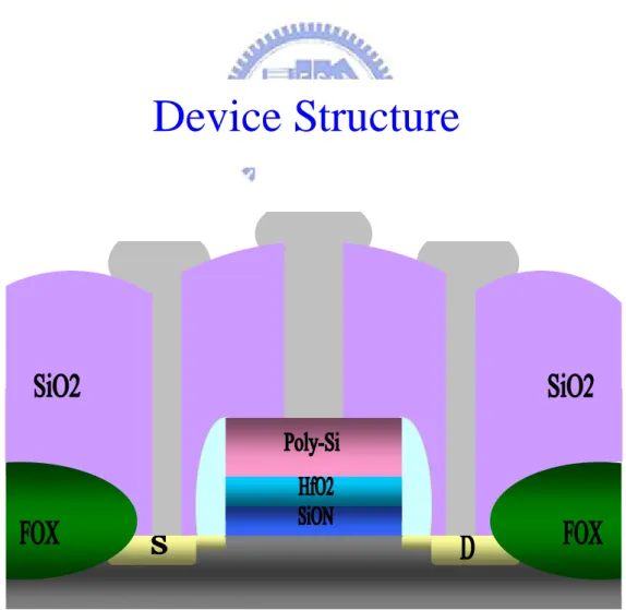
Standard local oxidation of silicon (LOCOS) process was applied to devices
isolation. The pMOSFETs were fabricated on 6-inch p-type (100) Silicon wafer utilizing conventional self-align process. After LOCOS was made and then fluorine (5E13cm-2) was incorporated by ion implantation, the schematic diagram is shown in Fig. 2-1, which to see if fluorine affects device performance and reliability compared with control sample (non-fluorine). After stripping sacrificial oxide by dipping in HF solution for seven minutes, standard RCA clean was used to remove the organics, particles and metal contamination. Immediately, a thin interfacial layer SiON was formed by Horizontal Furnace at 800℃ in NH3 and O2 ambient in order to avoid
negative oxide growing before depositing high-k dielectric and decrease leakage current. The SiON film was about 0.7nm~0.11nm, which was measured by ellipsometer. And then 3nm HfO2 film was deposited by ALCVD, following by RTA
-7-
at 600℃ for 30s in N2 ambient to improve the quality of high-k dielectrics. A 200nm
poly-silicon was deposited by low pressure chemical vapor deposition (LPCVD) . Subsequently, gate electrode was defined by I-line lithography stepper and etched by ECR etching system. After removing sidewall polymer, S/D extension implantation was implemented by B implantation. Spacer formation was carried out by plasma-enhance chemical vapor deposition (PECVD) and then S/D implantation was executed by Boron implantation. After S/D implantation, rapid thermal anneal (RTA) was performed at 950℃ for 20s in N2 ambient to activate dopants. Afterward, SiO2
capping layer was deposited by PECVD and contact hole pattering . And Al-Si-Cu metallization was deposited by PVD system and then pattering. Finally, forming gas annealing at 400℃ for 30 minutes in N2/H2 ambient .
2-2.1Measurement Setup
Current-voltage (I-V) and capacitance-voltage (C-V) characteristics were evaluated by a HP4156A precision semiconductor parameter analyzer and an HP4284 LCR meter, respectively. The equivalent oxide thickness (EOT) of the gate dielectrics was obtained from high frequency (100 KHz) capacitance-voltage (C-V) curve at strong inversion without considering quantum effect. The main process flow is summarized in Fig. 2-2 and schematic cross section of pMOSFETs with HfO2/SiON gate stack in
-8-
In this thesis, the interface trap density (Nit) was analyzed using the charging
pumping method. Square-wave waveforms (f=1MHz) which generated from 8110A were applied to the gate, and the base voltage was varied from inversion to accumulation, while keeping the pulse amplitude at 1.5V. Fig. 2-4 shows the configuration of measurement setup used in our charging pumping experiment. A MOSFET with gate area AG gives the charging pumping current as:
Icp =qAGNit (2-1)
The hole mobility for pMOSFETs was obtained by split C-V method. We know that drain current is a combination drift and diffusion currents as follows:
n eff n DS D eff Wu Q V kT dQ I Wu L q dx = − (2-2)
The effective mobility for pMOSFETs was measured at low drain voltage (about -50mv or -100mv), because then the channel charge is more uniform from source to drain, allowing the diffusive second term as below
n d eff g L u WQ = (2-3) where the drain conductance gd is defined as
. D V d GS DS I g const V ∂ = = ∂ n
Q was direct measured from capacitance measurements. The capacitance meter is
connected between the gate and the source/drain connected together with the substrate grounded. Therefore, Q was expressed as follows n
-9- GS V n GC GS Q − C dV ∞ =
∫
(2-4) and the vertical surface electric field εeff , was expressed as0 b n eff s Q Q K η ε ε + = (2-5) GS fb V b V GB GS Q =
∫
C dVwhere Q and b Q were charge densities (C/cmn 2) in the space-charge region and the inversion layer , respectively. The parameter η=1/3 was for hole mobility. We finally can calculate universal mobility by following equation
, 5 180 1 ( / 4.5 10 ) p eff eff u ε = + × (2-6)
We can extract mobility, universal mobility , effective field by above equation. Fig. 2-2 is the configure of split-CV measurement setup.
2-3 Result and Discussion
2.3-1. Electrical characteristics of pMOSFETs with and without
fluorine incorporation
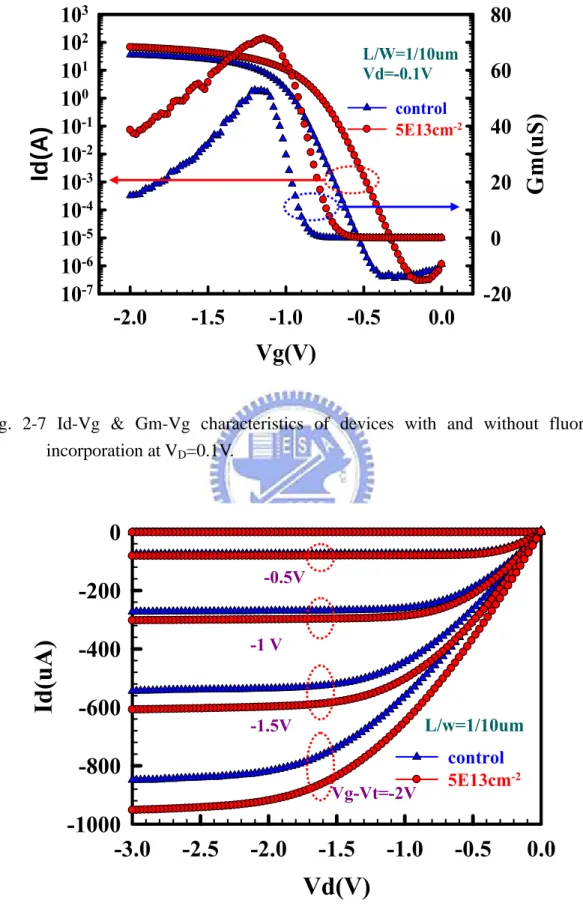
The C-V curves in Fig. 2-6 indicate not obvious change of EOT with and without fluorine sample, this means that fluorine atoms doesn’t break Hf-F bond and then causes dielectrics degradation [10]. And we can also observe that C-V curve in F-incorporated sample show shift toward positive Vg direction. Similar phenomenon
-10-
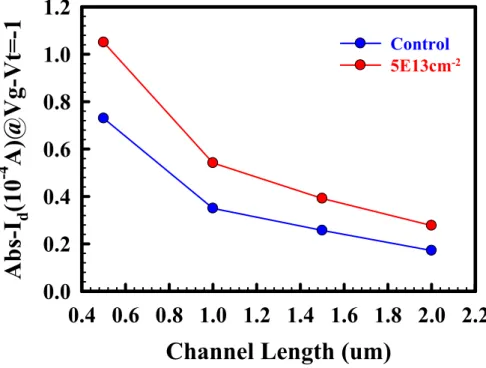
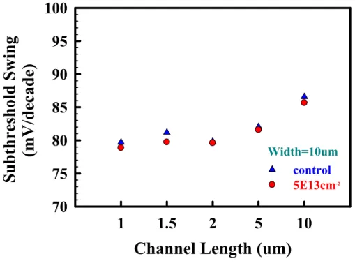
of positively charged traps or increase of negatively charged traps [8, 9, 13]. In Fig. 2-7 and Fig. 2-8 we also observe both drain current and transconductance have a apparent improvement in F-incorporated sample. Fig. 2-9 and Fig. 2-10 depict the results of driving current and maximum transconductance versus different channel length. When channel length becomes shorter, the improvement is more apparent. Fig. 2-11 indicates the sub-threshold swing for devices with and without fluorine incorporation. We find that sub-threshold swing versus channel length. We find that sub-threshold swing in F-incorporated sample is smaller than it in control sample. This implies that this dose of fluorine doesn’t cause severe damage in silicon bulk, on the other hand it makes the interface better. Fig. 2-12 shows the threshold voltage versus channel length. Threshold voltage shift toward positive Vg direction was also
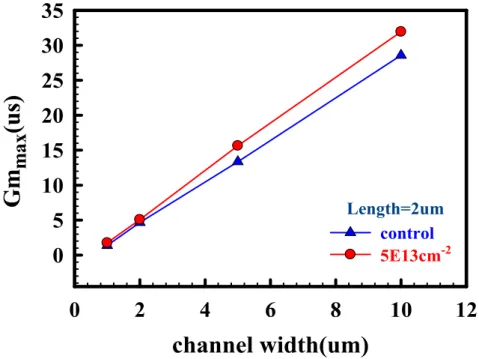
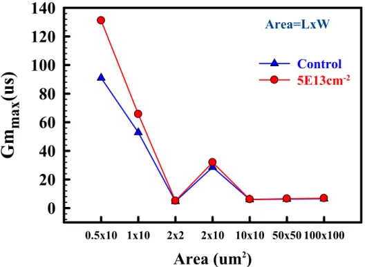
observed in F-incorporated sample. Fig. 2-13 and Fig2-15 show the maximum transconductance versus various channel width and area .Fig. 2-14 and Fig. 2-16 show the threshold voltage versus diverse channel width and area. We can see that F-incorporated sample has obvious improvement on maximum transconductance no matter in different channel length, width and area. And threshold voltage shift toward positive Vg direction also observe in F-incorporated sample. The driving current and transconductance of F-incorporated are higher than control sample. This is because less interface state existed in F-incorporated sample, and the higher mobility we get.
-11-
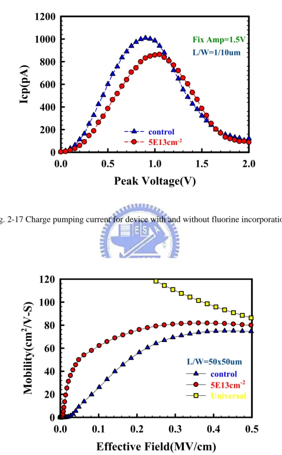
We can prove that by charge pumping method, in Fig 2-17. express charge pumping current for device with and without fluorine incorporation. We observe that charge pumping current decreases in F-incorporated sample. This implies a lot of dangling bond could be fixed by fluorine ion and therefore reduces interfacial layer. And then we can extract the value of Nit by equation (2-1). Then we get Nit values of
6.3067x1010cm-2 and 5.3926x1010 cm-2 with and without fluorine incorporation respectively.
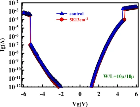
Fig. 2-18 shows that mobility versus effective electric field, we find the higher mobility we get in F-incorporated sample. This is also caused by fluorine ion fixed dangling bond in the interfacial layer. But using split-CV method wouldn’t calculate short channel device because we the capacitance is too small and disturbance is too large, then we can’t get it by HP4284 LCR meter. Therefore, we only can measure the large dimensional device. Fig 2-19 reveals that leakage current seems not to be increased for device with and without fluorine incorporation.
2.3-2. Conduction mechanism of pMOSFETs with HfO
2/SiON
gate stack
The carrier type involved in the leakage current through HfO2/SiON dielectric
-12-
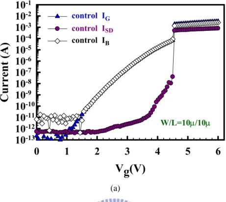
method [14]. The contributing carrier of the gate leakage current can be separated into holes and electrons. Fig. 2-20 shows carrier separation results under the inversion region, and Fig. 2-21 shows carrier separation results under the accumulation region for P+-gated PMOSFETs with HfO2/SiON gate stack, both with and without fluorine
incorporation. It is found that the source/drain current ISD dominates the leakage
current under inversion region, and the substrate current IB dominates the leakage
under accumulation region. This indicates holes from S/D that tunnel through gate dielectric is the dominant component of conduction mechanism under inversion region , while electrons from gate electrode that tunnel through gate dielectric is the dominant component of conduction mechanism under accumulation region.
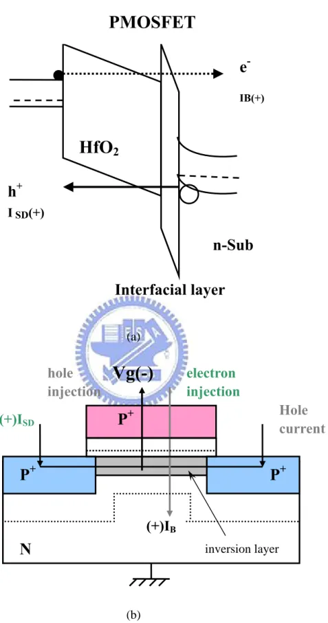
This could be explained by band-diagrams shown in Fig. 2-22(a) and carrier separation experiment shown in Fig. 2-22(b). The substrate current IB corresponds to
the electron current from the gate , while the source/drain current ISD corresponds to
the hole current from Si substrate under inversion region. Electron supply from the gate conduction band in pMOSFETs is limited by the generation rate of minority electrons in p+ gate. In other words, the probability of carriers from S/D that tunnel through gate dielectric is strongly affected by tunneling distance and barrier height [15]. Because of the asymmetry of the HfO2/SiON band structure , it is more difficult
-13-
hole current from the channel is the predominant injection current under stressing. The leakage component under accumulation region can also be explained by band-diagrams shown in Fig. 2-23(a), and the current component flow in carrier separation experiment is shown in Fig. 2-23(b).
In Fig. 2-24 and Fig. 2-25 , the gate current Ig as a function of Vg for the
HfO2/SiON layer is measured from temperature up to 125℃, both under inversion region and accumulation region for two samples. The current is temperature dependent that increases with increasing temperature. This implies that the conduction mechanism of current is trap-related, i.e., trap-assisted tunneling (TAT). Frenkel-poole, etc.
The gate leakage current for devices with HfO2/SiON gate stack is composed of
two types of current, i.e., hole current and electron current. To determine the conduction process in the HfO2/SiON dielectric, Frenkel-poole (F-P) plots are fitted
for hole current and electron current, respectively, for both samples. The current from Frenkel-poole emission is of the form:
2 exp( B) B q a V I V n k T Φ ∝ − (2-7) 0 ( / exp( B ox ins ) ox B q qE J B E k T πε ε − Φ − = ∗ (2-8) 0 / ln( ) ox ins B) ox ox B B q qE q J E E k T k T πε ε Φ = − (2-9)
-14- ⇒ intercept gives the Barrier height ( B
B
q k T
Φ − )
where B is a constant in terms of the trapping density in the HfO2 film , ΦB is
the barrier height, Eox is the electric field in HfO2 film. ε0 is the free space
permittivity, εinsis HfO2 dielectric constant, kB is Boltzmann constant , and T is the
temperature measured in Kelvin.
As shown in Fig. 2-26 and Fig. 2-27, under inversion region, excellent linearity for each current characteristic has been observed for both samples. This tendency indicates that both samples exhibit the Frenkel-Poole conduction mechanism for the gate leakage current. Both the electron and hole conduction mechanisms are the same, and the result agree well with the F-P conduction mechanism. Barrier height ΦB and
dielectric constant εinsof HfO2/SiON can be calculated. The εHfO2valre is found to be
~ 14.7 and ~14.4 for the control and F-incorporated samples, respectively.
The ΦB for the hole traps in the control sample and F-incorporated sample is about
1.47eV and 1.51eV, respectively. On the other hand, for electron traps, the ΦB of the
control sample and F-incorporated sample are about 1.59eV and 1.62eV, respectively. The ΦBto be discussed in this chapter is the “effective" value that is representative
of the HfO2/SiON gate stack [15]. We consider the case when the injected carriers
flow across HfO2/SiON by hopping via the trap sites with energy barrier ΦB, whose
-15-
the energy level for traps in the control sample is similar to that of the F-incorporated sample, and the energy barrier ΦB for holes is clearly lower than that for electrons
about 0.12eV in both samples.
2-4 summary
In this work, the initial electrical properties of the devices are smaller affected by fluorine incorporation, such as absolute threshold voltage is smaller and CV curve shifts toward positive Vg direction. We verify that appropriate fluorine incorporation
doesn’t degrade the interface and dielectric quality, and it can enhance mobility and drive current of the device. We use carrier separation to verify that devices with and without fluorine incorporation, we found gate leakage current is the same with both devices. And conduction mechanism is Frankel-Poole emission.
-16-
Fluorine Channel Implantation
․ Standard LOCOS process
․ Fluorine implantation(Dose:5E13 Energy:10KeV)
Fig. 2-1 Fluorine incorporation via channel implantation F F F F F F F F F F F
-17-
․ Standard LOCOS process
․ Fluorine implantation(Dose:5E13 Energy:10KeV)
․ RCA clean and HF dip
․ 800℃ in NH3 ambient by furnace ~SiON 0.7nm ․ ALD of 30 nm HfO2
․ PDA 600℃ 20sec in N2 ambient
․ poly-Si deposition 200nm and pattering
․ Spacer , S/D extension , S/D implant
․ Dopant activation : 950℃ , 30s
․ Passivation layer : SiO2 400nm ․ Metallization : Al-Si-Cu 900nm
․ Forming gas sintering : 400℃ , 30min
Fig 2.2 The process flow of pMOSFETs with HfO2/SiON gate stack
Fig 2-3 Schematic cross section of pMOSFETs with HfO2/SiON gate stack.
-18-
Fig. 2-4 Basic experimental setup of charging pumping measurement. Switch HP 4156 GPIB n-substrate p+ Source p+ Drain p+ poly-Si h+ e -HP 81110A Pulse Generator Vr
-19- (a)
(b)
Fig. 2-5 Configuration for (a)gate-to-channel, and (b)gate-to-substrate capacitance measurement.
P
+P
+P
+N
P
+P
+P
+N
G
G
-20-
Vg(V)
-2
-1
0
1
2
C
ap
aci
ta
nc
e(
uF
/c
m
2 )
0.0
0.2
0.4
0.6
0.8
1.0
1.2
1.4
1.6
control 5E13cm-2 L/W=50/50um EOTINV w F 2.8nm 2.79nm wo F-21-
Fig. 2-7 Id-Vg & Gm-Vg characteristics of devices with and without fluorine incorporation at VD=0.1V.
Vd(V)
-3.0
-2.5
-2.0
-1.5
-1.0
-0.5
0.0
Id(uA)
-1000
-800
-600
-400
-200
0
control 5E13cm-2 L/w=1/10umFig 2-8 Id-Vd characteristics for devices with and without fluorine incorporation.
Vg(V)
-2.0
-1.5
-1.0
-0.5
0.0
Id
(A
)
10
-710
-610
-510
-410
-310
-210
-110
010
110
210
3Gm
(u
S
)
-20
0
20
40
60
80
control 5E13cm-2 L/W=1/10um Vd=-0.1V Vg-Vt=-2V -1.5V -1 V -0.5V-22-
Channel Length (um)
0.4 0.6 0.8 1.0 1.2 1.4 1.6 1.8 2.0 2.2
Abs-I
d(10
-4A)@Vg-Vt=-1
0.0
0.2
0.4
0.6
0.8
1.0
1.2
Control 5E13cm-2Fig. 2-9 Compared Idlinear with channel length for device with and without fluorine.
0.4 0.6 0.8 1.0 1.2 1.4 1.6 1.8 2.0 2.2
20
40
60
80
100
120
140
control 5E13cm-2Channel Length (um)
Gm
ma
x
(us)
Fig. 2-10 Compared Gmmax with different channel length for device with and without
-23-
Channel Length (um)
1
1.5
2
5
10
Subthreshold Swing (mV/
decad
e)
70
75
80
85
90
95
100
control 5E13cm-2 Width=10umFig. 2-11 Compared sub-threshold swing with different channel length for device with and without fluorine.
0.4 0.6 0.8 1.0 1.2 1.4 1.6 1.8 2.0 2.2
Vth(V)
-1.1
-1.0
-0.9
-0.8
-0.7
-0.6
-0.5
controal 5E13cm-2 width=10umChannel Length (um)
Fig. 2-12 Compared threshold voltage with channel length for device with and without fluorine.
-24-
channel width(um)
0
2
4
6
8
10
12
Gm
ma x(us)
0
5
10
15
20
25
30
35
control 5E13cm-2 Length=2umFig. 2-13 Compared Gmmax with channel width for device with and without fluorine.
Width(um)
0
2
4
6
8
10
12
Vt
h(
V)
-1.1
-1.0
-0.9
-0.8
-0.7
-0.6
-0.5
control 5E13cm-2 Length=2umFig 2-14 Compared threshold voltage with channel width for device with and without fluorine.
-25-
Area (um
2)
0.5x10 1x10 2x2 2x10 10x10 50x50 100x100Gm
max
(us)
0
20
40
60
80
100
120
140
Control 5E13cm-2 Area=LxWFig. 2-15 Compared Gmmax with area for device with and without fluorine.
Area(um
2)
0.5x10 1x10 2x2 2x10 10x10 50x50 100x100Vth(V)
-1.2
-1.0
-0.8
-0.6
-0.4
Contral 5E13cm-2 Area=LxWFig. 2-16 Compared threshold voltage with area for device with and without fluorine.
-26-
Peak Voltage(V)
0.0
0.5
1.0
1.5
2.0
Icp(pA)
0
200
400
600
800
1000
1200
control 5E13cm-2 L/W=1/10um Fix Amp=1.5VFig. 2-17 Charge pumping current for device with and without fluorine incorporation.
L/W=50x50um
Effective Field(MV/cm)
0.0
0.1
0.2
0.3
0.4
0.5
Mobility(cm
2/V-S)
0
20
40
60
80
100
120
control 5E13cm-2 Universal L/W=50x50umFig. 2-18 Compared hole mobility with effective field for device with and without fluorine.
-27-
Vg(V)
-6
-4
-2
0
2
4
6
Ig
(A
)
10
-1210
-1110
-1010
-910
-810
-710
-610
-510
-410
-310
-2 control 5E13cm-2 W/L=10µ/10µFig. 2-19 Gate leakage current versus gate bias for fresh p-channel devices at room temperature.
-28- `
Vg(V)
-6
-5
-4
-3
-2
-1
0
Current(A)
10
-1210
-1110
-1010
-910
-810
-710
-610
-510
-410
-310
-2 control IG control ISD control IB W/L=10µ/10µ (a)Vg(V)
-6
-5
-4
-3
-2
-1
0
Current(A)
10
-1210
-1110
-1010
-910
-810
-710
-610
-510
-410
-310
-2 5E13cm-2 I G 5E13cm-2 ISD 5E13cm-2 I B W/L=10µ/10µ (b)Fig. 2-20 Carrier separation under inversion region (a) control sample, and (b)with F sample.
-29-
Vg(V)
0
1
2
3
4
5
6
Current (A)
10
-1310
-1210
-1110
-1010
-910
-810
-710
-610
-510
-410
-310
-210
-1 control IG control ISD control IB W/L=10µ/10µ (a)Vg(V)
0
1
2
3
4
5
6
Current(A)
10
-1310
-1210
-1110
-1010
-910
-810
-710
-610
-510
-410
-310
-2 5E13cm-2 I G 5E13cm-2 I SD 5E13cm-2 I B W/L=10µ/10µ (b)Fig. 2-21 Carrier separation under accumulation region (a) control sample, and (b)with F sample.
-30- (a)
(b)
Fig. 2-22 p+-gated pMOSFET with HfO2/SiON gate stack under inversion region (a) band diagrams, and (b) Schematic illustration of carrier separation experiment.
PMOSFET
p
+Gate
HfO
2e
- IB(+)h
+ I SD(+)n-Sub
Interfacial layer
P
+P
+P
+Vg(-)
electron
injection
Hole
current
hole
injection
(+)I
SD(+)I
BN
inversion layer-31- (a)
(b)
Fig. 2-23 p+ -gated pMOSFET with HfO2/SiON gate stack under accumulation region
(a)band diagrams , and (b)Schematic illustration of carrier separation experiment.
P
+P
+P
+Vg(+)
electron
injection
Hole
current
hole
injection
(-)I
SD(-)I
BN
inversion layerPMOSFET
p
+Gate
HfO
2e
-I
B(-)
h
+ ISD(-)n-Sub
Interfacial layer
-32-
V
g(V)
-6
-4
-2
0
2
4
6
I
g(A)
10
-1210
-1110
-1010
-910
-810
-710
-610
-510
-410
-310
-2 25oC 75oC 100oC 125oC Control W/L=10µm/10µmFig. 2-24 Gate leakage current versus gate bias without fluorine incorporation for fresh p-channel devices at different temperature.
V
g(V)
-6
-4
-2
0
2
4
6
I
g(A)
10
-1210
-1110
-1010
-910
-810
-710
-610
-510
-410
-310
-2 25oC 75oC 100oC 125oC W/L=10µm/10µm 5E13cm-2Fig. 2-25 Gate leakage current versus gate bias with fluorine incorporation for fresh p-channel devices at different temperature.
-33-
3600
3700
3800
3900
4000
4100
-30
-28
-26
-24
-22
-20
ln(J
SD/E)
E
1/2(V/cm)
1/2 25oC 75oC 100oC 125oC Frankel-poole emission W/L=10µm/10µm ΦB=1.47ev control (a)E
1/2(V/cm)
1/23600
3700
3800
3900
4000
4100
ln(J
SD/E)
-30
-28
-26
-24
-22
-20
25oC 75oC 100oC 125oC Frankel-poole emission W/L=10µm/10µm 5E13cm-2 ΦB=1.51ev (b)Fig. 2-26 conduction mechanism for source/drain current fitting under inversion region (a) without fluorine sample (b) with fluorine sample.
-34-
E
1/2(V/cm)
1/23600
3700
3800
3900
4000
4100
ln(J
B/E)
-30
-28
-26
-24
-22
-20
-18
-16
25oC 75oC 100oC 125oC Frankel-poole emission W/L=10µm/10µm control ΦB=1.59ev (a)E
1/2(V/cm)
1/23600
3700
3800
3900
4000
4100
ln(J
B/E)
-30
-28
-26
-24
-22
-20
-18
-16
25oC 75oC 100oC 125oC Frankel-poole emission W/L=10µm/10µm 5E13cm-2 ΦB=1.62ev (b)Fig. 2-27 conduction mechanism for substrate current fitting under inversion region (a)without fluorine sample (b) with fluorine sample.
-35-
Chapter 3
Impacts of Fluorine Incorporation on the
Reliability of pMOSFETs with HfO
2/SiON
Gate Stack
3-1 Introduction
The main issue of reliability in pMOSFETs is NBTI (negative bias temperature
instability) [17-18-19]. It manifests itself as a increase in the absolute threshold voltage, and a decrease in the inversion layer mobility under the negative bias at elevated temperatures. This is due to increase in interface states and generation of positive charges during NBTI processes. The device parameter degradations can lead to circuit failures, both for analog and digital application. The mechanism of NBTI is the depassivation of Si-H bonds at Si/SiON interface.
Unlike SiO2 films, high-k films have another problem, charging trapping . Charge
trapping causes the threshold voltage to shift with stressing time, and is therefore an important transistor reliability issue. Two mechanisms: the depassivation of Si-H bonds and trapping effect for pMOSFETs with high-k gate dielectric.
Fluorine is known as to worsen boron penetration in PMOS devices employing p+ gate. Therefore fluorine incorporation has been generally regarded as undesirable
-36-
for PMOS device application. Nevertheless, an appropriate fluorine implant will enhance oxide reliability.
Huard et al. has demonstrated that the use of BF2 implants , in lieu of B implants ,
for the S/D and poly gate for the traditional p+-gated pMOSFETs with nitrided gate oxide layer results in lower device degradation. Fluorine was found to improve the gate oxide reliability as long as the concentration is moderate. This result has been confirm by deliberate fluorine implantation, in addition to BF2 doping, which also
shows alleviated NBTI degradation [20].
In this thesis, effects of fluorine (F) on the reliabilities of pMOSFETs with HfO2/SiON have been studied. We incorporate fluorine ions via channel implantation ,
and we found that F-incorporated sample improving NBTI immunity. The reliability of pMOSFETs with and without fluorine incorporation will discuss in this later.
3-2 The Models of NBTI and the Mechanism of Fluorine
Incorporation Alleviate NBTI Degradation
3-2.1 The Models of NBTI
The model about negative bias stress (NBS) was first published by Jeppson and Svensson in 1977 [21-22]. This is so call Reaction-Diffusion model, which can be
-37- generalized as
+
-interface
(interface defect)
(interface trap) + (fixed oxide charge) X +e ←⎯→ + (3-1) interface diffusion bulk X ←⎯⎯⎯→X (3-2) where X represents a mobile species which diffuse away from the interface. It is noted that interface defect in Eq. (3-1) means Si/SiO2 or Si/high-k interface is comprised of hydrogen passivating Si dangling bond and that X is hydrogen (atom or proton) or some water-related species[17,22,23]. The interface trap is then supposed to be a silicon dangling bond denoted as Si․ which results when H is removed from Si-H bond. A detailed critical analysis of the proposed reactions has been given in [21,24] Their model forms the basis for models subsequently modified by others.
Other models like hydrogen models are used to explain NBTI. They are: (a)high electric fields induced SiH dissociation model , as follows
0
3 3
Si ≡SiH ⎯⎯→Si ≡ • +Si H (3-3) where H0 is a neutral interstitial hydrogen atom or atomic hydrogen .
(b)interstitial atomic hydrogen attack model , as follows
Si3 ≡SiH +H+ ⎯⎯→Si3≡ • +Si H2 (3-4) according to the first-principles calculations show that the positively charged hydrogen or proton H+ is the only stable charge state of hydrogen at the interface and
-38-
that H+ reacts directly with the SiH to form an interface trap. This model uses the fact that the Si-H complex is polarized such that a more negative charge resides near the hydrogen atom. Mobile positive H+ migrates toward the negatively charged dipole region or the Si-H molecule. The H+ atom then reacts with the H- to form H2 leaving
behind a positively charged Si dangling bond.
(c) holes induce Si-H dissociation model , as follows
3 3
Si ≡SiH +h+⎯⎯→Si ≡ • +Si H+ (3-5) SiH interact with “hot holes” or holes near the Si/SiO2 interface during NBTI stress.
The fixed charge (Qf) is a by-product of trivalent Si defect near the SiO2/Si interface
oxide and also contributes to the shift of threshold voltage
0
3 3
O ≡SiH +h+⎯⎯→O ≡Si++H . (3-6) The generation of fixed charges is independent of oxide thickness, while the interface trap generation is inversely proportional to oxide thickness [21]. This suggests that NBTI is worse for thinner oxide, but this phenomenon is not always observed and highly dependent on the process conditions.
As proved by Jeppson and Svensson [22], the behavior of the interface trap generation suggests the generation process is diffusion controlled. Nit buildup equals
the total number of released H species. Hole-assisted reaction breaks interfacial SiH bonds, resulting in Nit generation:
-39-
( ) ( )n
it
N t R Dx t
∆ = (3-7) Although reaction-diffusion model can predicts the threshold voltage shift to increase with a power law dependence on time. However, the model does not predict the saturation as observed after prolonged stressing nor does it derive the dependence of ∆ on stress oxide field from first principles. In 2004 , Sufi Zafar from IBM Vt
proposed a physical based model for NBTI induced degradation [25]. This model attributes NBTI to depassivation of Si-H bonds at the SiO2/Si interface. The two
distinguishing features of the proposed model are: (i) statistical mechanics is applied to calculate the decrease in interfacial Si-H density as a function of stressing conditions, and (ii) hydrogen diffusion in the oxide is assumed to be dispersive and the diffusing species is identified with the positively charged hydrogen ion (Hi+). The model assumes that as Hi+ diffuses away from the interface into the oxide, interfacial and bulk traps are created. Based on these model assumptions,an equation .for ∆ Vt
shift is derived as a function of stress time, oxide field, temperature, oxide thickness, and initial Si-H density at the interface. The equation as follows
∆V tt( )= ∆Vmax (1⋅ −e−( / )t τ β) (3-8) where, ∆Vmax, τ , β are the model parameters. According this model, we can explain NBTI mechanism in conventional dielectrics completely.
-40-
dielectrics is more serious. This is because that high-k film is a big trapping center compared to SiO2 [1] . Although Si-H dissociation is one of the reason of threshold
voltage shift, but the main reason of Vth shift is charge injection [26]. This indicate the
threshold voltage shift is bulk fixed charges dominative, not interface defects.
3-2.2 The Mechanism of Fluorine Incorporation Alleviate NBTI
Degradation
Fluorine incorporation technique was widely studied in 1980s. Wright and Saraswat, their research point out that fluorine incorporation will improve interfacial layer quality [10]. This is because fluorine can passivate the interface defects by forming Si-F bond, and lead to higher reliability. But the research also indicated that large concentrations of fluorine can cause deterioration of bulk gate oxide, although the interfacial region is improved.
In this work, we incorporated fluorine via channel implantation. We found that most of the fluorine atoms implanted in the channel are diffused into HfO2 layer after
annealing [9]. Fluorine is believed to form stronger Si-F bonds (5.73eV) compared to Si-H bonds (3.18eV) in the SiON/Si interface [8], and then improved interface quality and has NBTI immunity. A large number of fluorine exited in the high-k bulk is expected to reduce the defect density and thus reduce charge trapping by bonding to
-41-
Hf dangling bond resulting in annihilation of oxygen vacancies. As show in Fig. 3-2 , we schematic describe the binding of Si-F bonds and Hf-F bonds.
3-3 Measurement Setup
Constant voltage stress (CVS) is method to evaluate the reliability of devices as it causes threshold voltage to shift with electrical stressing. A constant voltage stress is applied to device gate from Vg=-2V~-3V, while source/drain and substrate are
grounded.We measurement Id-Vg and charging pumping during stress intervals.
Id-Vg measurements are used to evaluate Gm variation and threshold voltage shift.
And charging pumping measurements are used to obtain interface density generation. Moreover, the total trap density which consists of interface trap density and bulk trap density is calculated from threshold voltage shift before and after stress. It expresses as follows
/
total th G
N C V qA
∆ = ∆ (3-9) and bulk trap density also can be calculated as follows
bulk total it
N N N
∆ = ∆ − ∆ (3-10)
Negative bias temperature instability (NBTI) is an important reliability issue as it causes the threshold voltage to shift with electrical stressing at elevated temperature. To evaluate device degradations due to the bias temperature stress (BT), the gate
-42-
electrode of the device was subjected to stress condition with negative bias (-3V) varying from 25℃ to 125℃, while the drain/source and substrate were all grounded. The detail process is the same as CVS process , except temperature variation. Fig. 3-3 shows the experimental framework of our measurements.
3-4 Reliability of Control and Fluorine-Incorporated
Devices
3-4.1 CVS of control and Flourine-Incorporated Devices
Fig. 3-4 (a) and Fig. 3-4 (b) expresses Id-Vg characteristics before stress and after
stress at 25℃. We observe that there is no severe degradation of sub-threshold swing but positive Vth shift after stress is observed. This means that interface state
generation plays no significant role, rather, charge trapping in the bulk dielectric is the primary mechanism leading to CVS issues in high-k dielectrics. Vth shift of the
control sample is found to be slightly larger.
The threshold voltage shift (ΔVth) is measured with respect to the Id-Vg
characteristics with and without fluorine incorporation shown in Fig. 3-5 in linear scale, and Fig3-6 in logarithm scale .The threshold shifts toward negative gate voltage (ΔVth < 0), thus implying that net positive charges are trapped in the gate dielectric
-43-
shows smaller ΔVth than the control sample under different stress voltages as shown
in Fig. 3-7. Fig. 3-6 shows that Vth degradation obeys the power law [22,27],
∆V tth( )= Atb (3-11)
and the exponential values of both samples at vg=-3V(0.076 for control sample, and 0.54 for fluorine sample) are much larger than those of the device at Vg=-2V(0.022 for control sample, and 0.013 for fluorine sample) . This indicates that Vth degradation
is more severe for the devices under larger constant voltage stressing. The exponential value is voltage dependent relative to bulk trap generation.
To further gain insights into the degradation mechanism during voltage stressing, the interface state generation, ΔNit, and the increase of effective total trap density,
ΔNtot, are plotted as a function of the stress time in Fig 3-8(a)control sample ,and
(b)fluorine sample ,respectively. Apparently, ΔNtot(=ΔNit+ΔNot) is significantly
larger thanΔNit, suggesting that the degradation under CVS is dominated by the
charge trapping in the bulk of HfO2 film, rather than the generation of interface states,
irrespectively of whether fluorine is added or not. The instability of HfO2/SiON gate
stack is mainly determined by the bulk charge traps, contrast to that in the SiON gate stacks. In addition, the improvement in charge trapping is larger than that in interface generation as shown in Fig. 3-9.
-44-
3-4.2 NBTI of Control and Flourine-Incorporated Devices
Fig. 3-10(a) and (b) expresses Id-Vg characteristics before stress and after stress at
125℃. Compared Fig. 3-4 (a) and (b), we found that there is observable change in S.S at high temperature, compared to that at room temperature, indicating that ΔNit
increases with increasing temperature. This phenomenon is consistent with our results as shown in Fig. 3-11.
Fig. 3-12 and Fig. 3-13 compare the NBT-Stress-time dependence of threshold voltage shift for HfO2/SiON gate stack with and without fluorine incorporation. A
significantly smaller Vth shift is observed for the F-incorporated sample under the BT stress,Vg=-3V at 25℃ and 125℃ as shown in Fig 3-14. Such phenomena can be
attributed to fluorine incorporation into gate dielectric. Fig. 3-14 also shows that the exponential values of both samples at 125℃ (0.106 for control sample and 0.093 for fluorine sample) are much larger than those of the devices at 25℃ (both about 0.056). This indicates that the Vth degradation could be more severe for the devices under BT
stress at high temperature [28]. The exponential value is temperature dependent relative to bulk trap generation.
Fig. 3-15(a) and (b) show ΔNtot as a function of time during NBTI for both devices
measured at different temperatures. It is found that for both devices, Vth degradation
-45-
control sample than in F-incorporated. Fig. 3-16 shows that F-incorporated sample has less ΔNtot than control sample, this means less degradation in F-incorporated sample.
Compared Fig. 3-11 with 3-15(b), we found that interface states is not the main reason of threshold voltage shift. This indicates that charge trapping in bulk is the main reason of threshold voltage shift. The research has pointed out that amount of bulk traps is one to two order higher than amount of interfacial traps [1].
3-5 Summary
In this work, we found F-incorporated sample has less degradation than control sample. From CVS measurements, the value of ΔNit is similar to that of traditional
SiO2 dielectric. And the exponential value of ΔVth is voltage dependent. From NBTI
measurements, the exponential value of ΔVth is voltage and temperature dependent.
As result, we can confirm that charge traps in the bulk of HfO2/SiON gate stack are
responsible for the instability. We can expect a continuous distribution of charge trapping cross sections, instead of a discrete-value capture cross section, in HfO2
high-k film [26]. A better interface is expected to help reduce Vth instability, therefore
bulk traps need to be reduced. Our experimental also results show that hole trapping is dominant in DC stress.
-46-
Fig. 3-1 SIMS profile of F and B atoms for as-implanted and after annealing with and without F implantation. (Ref[9])
-47-
Fig. 3-2 Fluorine diffuses into HfO2/SiON stack and forms stronger Si-F bonds
compared to Si-H bonds , and reduce charging trapping by bonding to Hf dangling bond result in annihilation of oxygen vacancies.
F-S Hf-F F-S Hf-F F-S Hf-F F-S F-S
Si(100
)
F diffusion HfO2 SiONPMOSFET
p+ Gate
-48-
Fig. 3-3 Basic measurement method for (a) CVS (constant voltage stress), and (b)NBTS (negative bias temperature stress).
n+ n+ n+ P G ID-VG & CP DC stress 10sec ….. Charge pumping: To evaluate △Nit ID-VG: To evaluate △Gm ID-VG & CP ID-VG & CP ID-VG & CP DC stress 5sec DC stress 1sec
CVS for gate electrode CVS = -2, -2.5, -3V △Vth & △Nit n+ n+ n+ P G ID-VG & CP DC stress 10sec ….. Charge pumping: To evaluate △Nit ID-VG: To evaluate △Gm ID-VG & CP ID-VG & CP ID-VG & CP DC stress 5sec DC stress 1sec
CVS for gate electrode CVS = -3V
Change T