行政院國家科學委員會專題研究計畫 成果報告
ZnO 奈米線之合成及其於平面場放射光源之應用研究
研究成果報告(精簡版)
計 畫 類 別 : 個別型 計 畫 編 號 : NSC 96-2221-E-151-021- 執 行 期 間 : 96 年 08 月 01 日至 97 年 07 月 31 日 執 行 單 位 : 國立高雄應用科技大學電子工程系 計 畫 主 持 人 : 楊素華 計畫參與人員: 碩士班研究生-兼任助理人員:黃士峰 碩士班研究生-兼任助理人員:王千鴻 碩士班研究生-兼任助理人員:陳保志 碩士班研究生-兼任助理人員:洪勝裕 報 告 附 件 : 出席國際會議研究心得報告及發表論文 處 理 方 式 : 本計畫可公開查詢中 華 民 國 97 年 10 月 31 日
行政院國家科學委員會補助專題研究計畫
成 果 報 告
□期中進度報告
ZnO 奈米線之合成及其於平面場放射光源之應用研究
計畫類別: 個別型計畫
□ 整合型計畫
計畫編號:NSC
96-2221-E-151-021-
執行期間:
96 年 08 月 01 日至 97 年 07 月 31 日
計畫主持人:楊素華
共同主持人:
計畫參與人員:陳保志,洪勝裕,黃士峰,王千鴻
成果報告類型(依經費核定清單規定繳交):精簡報告 □完整報告
本成果報告包括以下應繳交之附件:
□赴國外出差或研習心得報告一份
□赴大陸地區出差或研習心得報告一份
出席國際學術會議心得報告及發表之論文各一份
□國際合作研究計畫國外研究報告書一份
處理方式:除產學合作研究計畫、提升產業技術及人才培育研究計畫、
列管計畫及下列情形者外,得立即公開查詢
□涉及專利或其他智慧財產權,□一年□二年後可公開查詢
執行單位:國立高雄應用科技大學
中
華
民
國
97
年
10
月
日
I. Abstract
In this study, field emission characteristic of the silver-catalyzed ZnO nanostructure grown on silicon by vapor-phase transport process was investigated. The ZnO nanostructures were grown on different temperature and time. The structure and optical properties of ZnO nanostructures were investigated using scanning electron microscopy SEM, X-ray diffraction X-ray and photoluminescence analyses. X-ray diffraction measurements showed that the main grown plane of ZnO nanostructures was (002) plane. The ZnO nanostructure has diameters ranged from 50−200 nm and length from 2−4μm.Theoptimalfield emission property ofZnO nanorods was obtained when it was synthesized at temperature 680oC for 60 min at region C. The turn-on electric field for ZnO nanorods was 5.23 V/μm.When the electric field was 8.46V/μm and a phosphor screen was used as anode, the emission current density approached 20.5 μA/cm2. Bright phosphor image was observed from the diode mode field emission lighting.
中文摘要 本研究是利用氣相傳輸法並使用銀觸媒成長氧化鋅奈米柱的場發射特性探討及其於平 面場放射平面光源之應用研究。我們探討在不同溫度、時間下,所形成之氧化鋅奈米柱特 性。使用場發射掃描式電子顯微鏡以及 x-ray 和光激發光特性來探討氧化鋅奈米柱的結構與 光特性。經由 x-ray 量測可以得知氧化鋅奈米柱的主成長方向為(002)面。銀觸媒平均所成 長出之氧化鋅奈米柱的直徑為 50-200 nm,長度為 2-4 μm。所成長之氧化鋅奈米柱之最佳 場發射特性為在區域 C,成長溫度為 680 度,成長時間為 60 分鐘。起始電場為 5.23 V/μm。 在電場強度8.46 V/μm、螢光面為陽極時,所得之電流密度大約為 20.5μA/cm2。利用二極式 氧化鋅奈米結構可以順利激發螢光粉發光,即可完成氧化鋅奈米線平面場放射光源之製作。 II. Introduction
Nanostructures have attracted much attention owing to their peculiar and fascinating properties [1,2]. Since the discovery of carbon nanotubes in 1991 [3], one-dimensional (1D) nanostructures, including nanotubes [4-6], nanowires [7-9], and nanorods [10-12], are studied actively because of their unique physical properties and potential to revolutionize broad areas of nanotechnology. 1D nanostructures represent the smallest dimension structure that can efficiently transport electrical carriers, and thus are ideally suited to move charges in integrated nanoscale systems [13]. In addition, owing to quantum confinement, 1D nanostructures can demonstrate the characteristic of light emission [14]. Therefore, 1D nanostructures are expected to play an important role as both interconnects and functional units in electronic, optoelectronic, electrochemical, and electromechanical devices with nanoscale dimensions.
Recently, 1-D nanostructures such as wires, belts, rods, and tubes have also become the dominate research subjects owing to their unique applications in mesoscopic physics and fabrication of nanoscale devices. 1-D nanostructures, exhibiting photonic and electronic confinement in two-dimensions, have attracted considerable interest as potential candidates for a variety of nanoscale electronic and optoelectronic devise [15-18].
Zinc oxide is a highly complex material with some unique properties which give rise to many of its scientific and technical applications. Some especially properties of ZnO are: the anisotropy in crystal structure, the non-stoichiometric defect structure, the broad band gap, the high reflectivity in visible and strong absorption in ultraviolet, and dissociative sublimation and
amphoteric chemical behavior. Furthermore, ZnO is an environment-friendly material. It belongs to wurtzite structure in hexagonal system, with lattice constants a =b = 3.250 Å and c = 5.205 Å. The inherent n-type character of ZnO is caused by a deviation from stoichiometry due to intrinsic internal defects such as oxygen vacancies and zinc interstitial.
ZnO nanostructures have many applications, such as piezoelectric transducers, surface acoustic wave devices, gas sensors, varistors, phosphors, transparent conducting films, and field emitters for field emission lighting.
III. Experimental
p-type silicon was used assubstrate.Theelectricconductivity ofsilicon waferwas10Ω-cm. Silver (Ag, 99.995) was used as a catalyzst. ZnO (99.995) and graphite (99.999) were used as source powders. First, 7-nm-thick Ag thin film was evaporated on Si substrate at evaporation rate of 0.02 nm/s. After the evaporation of Ag film was finished, ZnO and graphite (weight ratio = 1:1) powders were put on an alumina boat, then placed at the center of a quartz tube. And other alumina boat carrying the Ag-deposited substrates were placed into the quartz tube as well. The substrates were placed at regions A, B, C and D from the center of the quartz tube. The flow rates of the nitrogen and oxygen were 70 and 20 sccm, respectively.
The system temperature for growing ZnO nanorods was set at 1050−1150oC. The substrates were located at four different places, which were named as region A, B, C and D. The temperature at region A is 1050−1150oC. The temperature at region B is 1020−1120oC. The temperature at region C is 580−680oC, and region D is room temperature. The growth time of ZnO nanorods was set at 10, 30 and 60 minutes. After the furnace was cooled to room temperature, dark gray material was obtained on the surface of the substrates.
Field emission scanning electron microscopy (FE-SEM, Philips XL40 FE-SEM). X-ray diffraction (XRD, SIEMENS D5000& ENRAF-NONIUS 852DX60D) and photoluminescence (PL, Hitachi F-4500, Japan) were used to evaluate the characterizations of crystal structure, surface morphology, chemical composition and optical properties of the ZnO nanostructures. Transmission electron microscopy (TEM, PHILIPS CM-200) was used to measurement a real space image on the atom distribution in the nano-crystal. The field emission measurements were implemented in a vacuum chamber with 5×10⁻⁶ Torr at room temperature. The phosphor coated ITO was used as field emission anode. The distance between anode and ZnO nanostructures was 130 μm.The ZnO nanostructure field emission lighting was made with diode type. Emission currents were characterized by the direct current (DC) mode. The field emission current-voltage characteristics were evaluated with a Keithley 2410 power source. CIE coordinates and illumination of devices were measured by CS-100A chroma meter.
III. Results and Discussion
3-1 ZnO nanorods grown in region A
Substrate was placed near source powders. The temperature of source powders was set at 1050−1150oC. The substrate temperature was fixed at 1050−1150oC. The grown time for ZnO nanorods was set at 10−60 min.
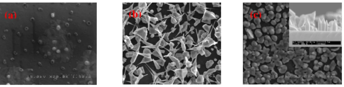
Figure 1 shows the SEM images of ZnO nanorods grown at 1050oC for 10, 30, and 60 minutes. It shows that when the growth time was short, insignificant growth of ZnO nanorods
was observed. When the growth time was increased from 10 minutes to 30 minutes, lots of ZnO nanorods were grown at 1050oC; however, when the growth temperatures were at 1100oC and 1150oC, no ZnO nanorods were grown. When growth temperature was at 1050oC for 60 min, nanorods were grown.
Fig. 1 shows the SEM images of ZnO nanorods grown at 1050oC for (a) 10, (b) 30, and (c) 60 minutes.
The XRD patterns in Fig. 2 show that the ZnO nanorods was a wurtzite structure. The lattice constants of ZnO nanorods were a = b = 3.26 Å and c = 5.22 Å. The strong (002)peak atθ= 34.4o and other small peaks originated from the hexagonal ZnO were observed. The main growth plane of ZnO nanorods was (002) for grown temperature at 1050oC. XRD data exhibited dominant peaks at 34.4o, 31.7oand 36.2owere corresponding to ZnO (002), (100) and (101) planes.
The optical properties of the ZnO nanorods were characterized by the PL spectra measurement at room temperature. In Fig. 3, it is not only the emission peak centered at 384 nm (3.23 eV) in UV band was measured for all the nanostructures, but also a broad green band (visible emission) with peaks at 493 nm (2.52 eV) was estimated. The UV emission band is due to a near-band-edge (NBE) transition of wide band gap of ZnO, namely the recombination of free excitons through an exciton–exciton collision process, while the green band emission is attributed to the radial recombination of a photogenerated hole with an electron that belongs to a singly ionized oxygen vacancy in the surface and subsurface lattices of the ZnO materials.
3-2 The ZnO nanorods grown in region B
The temperature of source powders was set at 1050−1150oC and the substrate temperature was at 1020−1120oC. The grown time was varied from at 10 to 60 min.
10 20 30 40 50 60 70 80 0 200 400 600 800 1000 Z n O (1 0 3 ) Z n O (1 1 0 ) Z n O (1 0 2 ) Z n O (1 0 1 ) Z n O (0 0 2 ) Z n O (1 0 0 ) 1150oC 1100oC 1050oC In te n si ty (a .u .) 2(degree)
Fig. 2 XRD patterns of ZnO nanorods Fig. 3 Spectrum of ZnO nanorod excited grown at 1050−1150oC for 60 min. at wavelength of 325 nm.
(a) (b) (c) 350 400 450 500 550 600 1000 2000 3000 4000 5000 6000 In te n si ty (a .u .) Wavelength (nm) 384 nm 493 nm
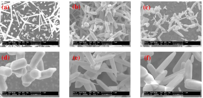
The SEM photographs of ZnO nanorods grown at substrate temperatures of 1020−1120oC are shown in Fig. 4. We found that no any ZnO nanorods were grown if the growth time was short. While increasing to 30 minutes, the growth of ZnO nanorods obviously increased (Figs. 4(a)−4(c)); the diameters of ZnO nanorods were about 100−500 nm and their lengths were about 2−4μm.When the Ag catalyst was not deposited, ZnO nanorods could be grown successfully. When temperature increases to 1150oC, the ZnO nanorod’s structure was changed form hexagonal to cylinder structure. The appearance of nanorods was changed as the substrate temperature was increased. The SEM photos for nanorods grown for 60 minutes are shown in Figs. 4(d)−4(f). The diameters of ZnO nanorods were about 300−500 nm and their lengths were about 2−4 μm. We found that when the growth temperature increased, the quantity of ZnO nanorods increased, in the meantime, when the growth time increased, the quantity of ZnO nanorods increased as well.
Fig. 4 SEM photographs of ZnO nanorods grown at (a) 1020, (b) 1070, (c) 1120oC for 30 min; (d) 1020, (e) 1070, (f) 1120oC for 60 min.
30 40 50 60 70 0 1000 2000 3000 4000 5000 6000 7000 (f) (e) (d) (c) (b) (a) (1 0 3 ) (1 1 0 ) (1 0 2 ) (1 0 1 ) (0 0 2 ) 1120oC 1070oC 1120oC 1070oC 1020oC In te n si ty (a .u .) 2(degree) 1020oC (1 0 0 ) A g (2 0 0 )
Fig. 5 XRD patterns of nanorods grown at different Fig. 6 EDX plot of nanorods grown substrate temperature. (a)−(c) without catalyst, (d) in region B.
−(f) with catalyst.
(b)
(c)
(d)
(f)
(a)
(e)
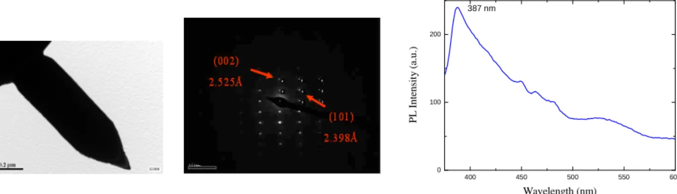
Energy (keV)XRD patterns shown in Fig. 5 reveal that the ZnO nanorods were a wurtzite structure. The lattice constants of ZnO nanorods werea= b = 3.26 Å and c = 5.22 Å.Thestrong (101)peak atθ = 36.3o and other small peaks originated from the hexagonal ZnO were observed. The main growth plane of ZnO nanorod was (101) for as-grown (non-catalyzed), but it was (002) for 7-nm-thick Ag film deposited.Thestrong peak atθ = 44.4oin Fig. 5(d) was referred to (200) Ag. The chemical composition of the ZnO nanorods grown on Si substrate was evaluated by energy dispersive X-ray fluorescence (EDX). Figure 6 shows that only Zn and O peaks were observed; the detected Si peak was come from Si substrate. TEM image of ZnO nanorod grown at 1020oC for 60 min shown in Fig. 7(a). Figure 7(b) is SAED image. ZnO nanorod (002) direction with the d-spacing of 2.525 Å was observed. The (101) direction shows that the d-spacing was 2.398 Å. From PL property shown in Fig. 7(c), it reveals that the nanorods grown at region B exhibited a better crystallinity. 400 450 500 550 600 0 100 200 P L In te n si ty (a .u .) Wavelength (nm) 387 nm
Fig. 7 (a) TEM image, (b) SAED image, (c) PL spectrum of nanorods grown at 1020oC for 60 min.
3-3 The ZnO nanorods grown in region C
The source temperature was set at 1050−1150oC and the substrate temperature was at 620−680oC. The growth time was 10−60 min.
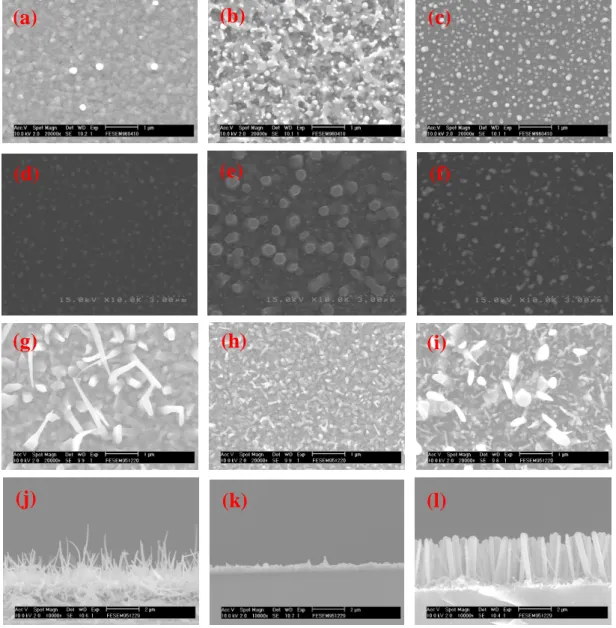
The surface morphologies of ZnO nanorods are shown in Fig. 8. We found that no any ZnO nanorods were grown up because of the short growth time, 10 min (Fig. 8(a)−(c)). While the growth time was increased to 30 minutes, nanorods were grown (Fig. 8(d)−(f)). While increasing the growing time to 60 minutes for a long time growth, the growth of nanorods were observed obviously. The diameters of ZnO nanorods were about 50−100 nm and their lengths were about 2−4μm, as shown in Fig. 8(g)−(i). The cross-section images of the ZnO nanorods grown at 620−680oC for 60 min were shown in Fig. 8(j)−(l), which revealed that the ZnO nanorods were almost vertically grown on Si substrate.
EDX analyses shown in Fig. 9(a) exhibited that only Zn and O peaks were observed. In addition, XRD pattern shown in Fig. 9(b) exhibited that the dominant peaks were at 34.4o, 31.7o and 36.2o, which were corresponding to ZnO (002), (100) and (101) planes. The strong (002) peak at 2θ= 34.4owere observed, this indicated that the main growth plane of ZnO nanorod was (002). The lattice constants of ZnO nanorod were a = b = 3.26 Å and c = 5.22 Å. PL spectrum in Fig. 9(c) shown that it is not only a weak UV band with peak at 376 nm a strong broad green band with peak at 493 nm were observed. Apparently, a lot of surface vacancies were involved in the ZnO nanorods.
Fig. 8 Surface morphologies of ZnO nanorods grown at (a) 620oC, (b) 650oC, and (c) 680oC for 10 min; (d) 620oC, (e) 650oC, and (f) 680oC for 30 min; (g) 620oC, (h) 650oC, and (i) 680oC for 60 min. Cross section images for nanorods grown at (j) 620oC, (k) 650oC, and (l) 680oC for 60 min. 10 20 30 40 50 60 70 80 0 200 400 600 800 1000 Z n O (1 0 3 ) Z n O (1 1 0 ) Z n O (1 0 2 ) Z n O (1 0 1 ) Z n O (0 0 2 ) Z n O (1 0 0 ) 680oC 650oC 620o C In te n si ty (a .u .) 2(degree) 350 400 450 500 550 600 650 0 1000 2000 3000 4000 5000 493 nm P L In te n si ty (a .u .) Wavelength (nm) 376 nm
Fig. 9 (a) EDX plot, (b) XRD, and (c) PL of ZnO nanorods grown in region C.
3-4 Field Emission Characteristics for ZnO nanorods
Electron field emission is a quantum mechanical tunneling phenomenon. Figure 2-1(a) shows the energy band diagram of the metal and vacuum system. The electron on Fermi-level (EF)
needs enough power to shake off the bind energy of surface into vacuum. If an external bias is
(b)
(c)
(e)
(f)
(a)
(g)
(h)
(i)
(l)
(k)
(d)
(j)
Energy (keV) (b) (c) (a)applied on the emitter surface, the electrons will be emitted from metal through the surface potential barrier into vacuum. In 1928, Fowler and Nordheim proposed the theory of field emission. The emission of electrons from a metal-vacuum interface in the presence of electric field normal to the surface was initially treated as a quantum mechanical tunneling process. The F-N equation is as follow:
E y Bv y t AE J 2 3 2 2 exp . (1)Where J is the current density (A/cm2), E is the applied electric field (V/cm),Φ isthework function of emitter. A and B are constants; A = 1.54×10⁻⁶, B = 6.83×10⁹ (V×eV-3/2×m-1), v(y) = 0.95-y2≒ 1, t2(y) ≒ 1.1. In addition,J I/, whereαis emission area; and E V /d, βis the local field enhancement factor at the emitting surface, d is the distance between cathode and anode. Then the F-N equation will be written as
V d B d V A I 32 2 2 2 exp (2) and, V d B d A V I 32 2 2 2 ln ln . (3)
Therefore, when d and Φ are fixed, we could evaluate the field emission characteristic of field emitters from F-N equation. To reduce the operation voltage of field emission devices, some approaches may therefore be taken: (1) Lower the work function of the materials (Φ). (2) Narrow the cone angle (increases β). (3) Protect the cathode from arc breakdown. (4) Find techniques to reproducibly sharpen the tips to the atomic level (increases β).
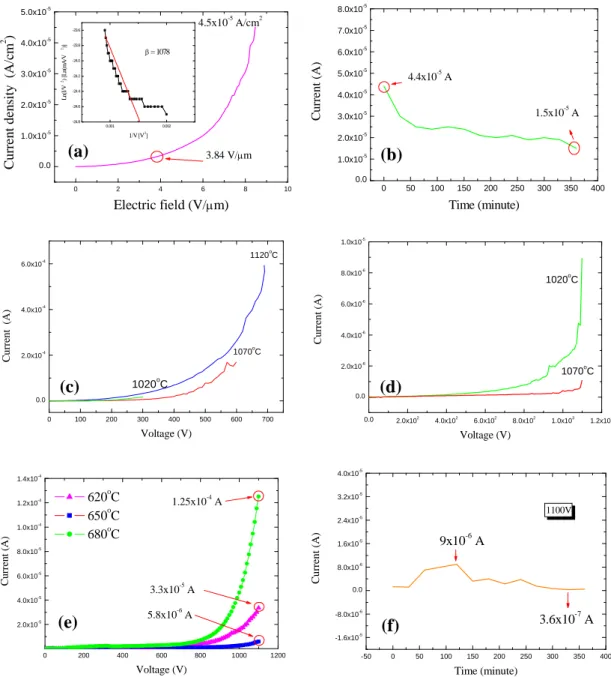
The field emission characteristics of the ZnO nanorods grown in regions A−C are shown in Fig. 10. For the ZnO nanorods grown in region A, the current of nanorods was 4×10⁻⁴A at 1100 V. The turn-on electricfield approaches3.84 V/μm in Fig 10(a); the measured current density was 45 μA/cm2 at 8.46 V/μm for ZnO nanorods grown at substrate temperature 1050oC for 1 hr. The electric field enhancement factor could be derived with formula of
b d B 32 95 . 0 , where b
is the slope of the F-N plot,
d B Slope b FN 2 3 .Thefield enhancementfactorβ wasabout1078
cm-1for ZnO nanorods grown at region A. The emission stability of ZnO nanorods grown at region A was measured at constant electric field of8.46 V/μm, as shown in Fig. 10(b). The max emission current density was 2.93μA/cm2and the min emission current density was 1 μA/cm2. The emission current density of ZnO nanorods emitter was approximately 1.93μA/cm2
after applying voltage for 6 h.
For the ZnO nanorods grown in region B, the emission current was 4.35×10⁻⁴A at 600 V for ZnO nanorods grown at 1020oC for 30 min, and the current was 7.11×10⁻⁴ A at 700 V for ZnO nanorods grown at 1070oC for 30 min. Both two samples can’t stand the high electric field strength. As the growth time increases, the I-V curves measured with ITO as anode for ZnO nanorods grown with silver-catalyzer at region B for 60 min was shown in Fig. 10(c). We find the current was 1×10⁻⁵ A at 300 V for ZnO nanorods grown at 1020oC for 60 min; the current was
0 2 4 6 8 10 0.0 1.0x10⁻⁵ 2.0x10⁻⁵ 3.0x10⁻⁵ 4.0x10⁻⁵ 5.0x10⁻⁵ C u rr en t d en si ty (A /c m 2 ) 0.001 0.002 -24.8 -24.6 -24.4 -24.2 -24.0 -23.8 -23.6 = 1078 L n( I/ V 2) [L n( m A /V 2)] 1/V[V-1 ] Electric field (V/m) 4.5x10⁻⁵A/cm2 3.84 V/m 0 50 100 150 200 250 300 350 400 0.0 1.0x10⁻⁵ 2.0x10⁻⁵ 3.0x10⁻⁵ 4.0x10⁻⁵ 5.0x10⁻⁵ 6.0x10⁻⁵ 7.0x10⁻⁵ 8.0x10⁻⁵ C u rr en t (A ) Time (minute) 4.4x10⁻⁵A 1.5x10⁻⁵A 0 100 200 300 400 500 600 700 0.0 2.0x10⁻⁴ 4.0x10⁻⁴ 6.0x10⁻⁴ C u rr en t (A ) 1120o C 1070oC Voltage (V) 1020oC 0.0 2.0x10² 4.0x10² 6.0x10² 8.0x10² 1.0x10³ 1.2x10³ 0.0 2.0x10⁻⁶ 4.0x10⁻⁶ 6.0x10⁻⁶ 8.0x10⁻⁶ 1.0x10⁻⁵ 1070o C C u rr en t (A ) Voltage (V) 1020oC 0 200 400 600 800 1000 1200 2.0x10⁻⁵ 4.0x10⁻⁵ 6.0x10⁻⁵ 8.0x10⁻⁵ 1.0x10⁻⁴ 1.2x10⁻⁴ 1.4x10⁻⁴ C u rr en t (A ) 5.8x10⁻⁶A 3.3x10⁻⁵A 1.25x10⁻⁴A Voltage (V) 620oC 650oC 680oC -50 0 50 100 150 200 250 300 350 400 -1.6x10⁻⁵ -8.0x10⁻⁶ 0.0 8.0x10⁻⁶ 1.6x10⁻⁵ 2.4x10⁻⁵ 3.2x10⁻⁵ 4.0x10⁻⁵ C u rr en t (A ) Time (minute) 9x10⁻⁶A 3.6x10⁻⁷A 1100V
Fig. 10 ZnO nanorods grown in (a) region A; region B (c) with catalyst and (d) without catalyst; (e) region C. The emission stabilities for nanorods grown in regions A and C are shown in (b) and (f) respectively. The inset in (a) is F-N plot.
1.6×10⁻⁴A at 600 V for ZnO nanorods grown at 1070oC for 60 min and the current was 5.9×10⁻⁴ A at 700 V for ZnO nanorods grown at 1120oC for 60 min. As the ZnO nanorods was grown without catalyzer (Fig. 10(d)), the current was 8×10⁻⁶ A at 1100 V for ZnO nanorods grown at 1020oC for 60 min, and the current was 1×10⁻⁶A at 1100 V for ZnO nanorods grown at 1070oC for 60 min.
For the ZnO nanorods grown in region C, the I-V curves is shown in Fig. 10(e) while using ITO anode and ZnO nanorods grown at substrate temperature of 620oC~680oC for 60 min. The emission current was 1.25×10⁻⁴ A at 1100V for ZnO nanorods grown at substrate temperature of 680oC. The current density was20.5 μA/cm2 at8.46 V/μm when the ZnO nanorods were grown substrate at temperature of 680oC for 1 hr. Thefield enhancementfactorβ wasabout1167cm-1 for the nanorods grown at region C. Furthermore, the emission stability of ZnO nanorods emitter was measured at constant electric field of8.46 V/μm.Thecurrentvariationas a function of time is shown in Fig. 10(f). The max emission current density was 25 μA/cm2 and the min emission
(a) (b)
(c) (d)
current density was 15 μA/cm2. The emission current density of ZnO nanorods emitter was approximately 20 μA/cm2after applying voltage for 6 h.
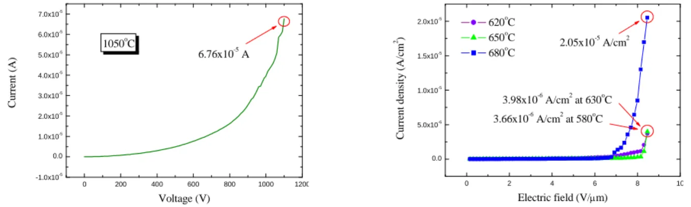
3-5 Luminescence Characteristics for field emission lighting
For the fabrication of field emission lighting, the ZnS:Ag,Cl phosphor coated ITO glass was used as anode. The emission current for the lighting was 6.76×10⁻⁵ A at 1100V for nanorod emitters grown in region A, as shown in Fig. 11(a). Furthermore, the emission current of the lighting for nanorod emitters grown in region C was measured as well. Fig. 11(b) shows that the emission current density for the lighting was 3.66 μA/cm2 at 8.46 V/μm when the nanorod emitters were grown at substrate temperature of 620oC for 1 hr. The turn-on electric field approaches4.92 V/μm and the current density for the lighting was3.66 μA/cm2 at8.46 V/μm
with a luminance of 39.29 cd/m2at 1100 V. In the meantime, we found that emission current was 3.98 μA/cm2at8.46 V/μmand the luminance was 34.87 cd/m2at8.46 V/μm fornanorod emitters grown at substrate temperature 650oC. The current density was20.5 μA/cm2at8.46 V/μm and the luminance was 291.4 cd/m2 at8.46 V/μm whilethenanorodemitters were grown at substrate temperature of 680oC. The cathodoluminescence (CL) image of the field emission lighting involved ZnO nanorod emitters together with a ZnS:Ag,Cl phosphor screen is shown in Fig. 12(a); the CIE coordinates were shown in the inset of Fig. 12(a). Fig. 12(b) is the luminance intensity
0 200 400 600 800 1000 1200 -1.0x10⁻⁵ 0.0 1.0x10⁻⁵ 2.0x10⁻⁵ 3.0x10⁻⁵ 4.0x10⁻⁵ 5.0x10⁻⁵ 6.0x10⁻⁵ 7.0x10⁻⁵ 6.76x10⁻⁵A C u rr e n t (A ) Voltage (V) 1050oC 0 2 4 6 8 10 0.0 5.0x10⁻⁶ 1.0x10⁻⁵ 1.5x10⁻⁵ 2.0x10⁻⁵ 3.66x10⁻⁶A/cm2at 580oC 3.98x10⁻⁶A/cm2at 630oC C u rr en t d en si ty (A /c m 2) Electric field (V/m) 620oC 650o C 680oC 2.05x10 -5 A/cm2
Fig. 11 Characteristics of the field emission lighting, (a) I-V plot for nanorod emitters grown at substrate temperature of 1050oC in region A; (b) J-E plot for nanorod emitters grown at different substrate temperature in region C.
0 150 300 10-6 10-5 10-4 C u rr en t (A ) Time (minute) 2.5x10⁻⁵ A 1.5x10⁻⁵ A 1100V
Fig. 12 (a) cathodoluminescence (CL) image of the field emission lighting, (b) luminance intensity of field emission lighting operated at different voltages. CIE coordinates and emission current stability are shown in the inset of Figs. 12(a) and 12(b), respectively.
0 200 400 600 800 1000 1200 0 50 100 150 200 250 300 291.4 cd/m2at 1100V 680oC L n m in a n ce (c d /m 2 ) Voltage (V)
for the field emission lighting operated at different voltages, where the ZnO nanorod emitters were grown at substrate temperature 680oC; the stability of emission current is shown in the inset of Fig. 12(b).
IV. Conclusions and comments
This study investigates the synthesis and field emission characteristics of zinc oxide (ZnO) nanostructures grown on Ag-depositeded Si substrate using vapor-solid mechanism. The morphology of ZnO nanostructures was related to source and substrate temperatures. A strong bluish-green photoluminescence indicated that the nanostructures had many surface defects correlated with oxygen vacancies. Field emission characteristic of the ZnO nanorods were evaluated. It shows that high emitter density and high aspect ratio of the nanorods resulted in an enhancement in emission current density. A better field emission stability of the nanorods was observed. In addition, the flat panel field emission lighting was prepared. A luminance of 291.4 cd/m2at 1000 V was obtained when the nanorod emitters were grown at substrate temperature of 680oC. The emission characteristics of the nanostructures and the luminescence properties of the field emission lighting have to be improved; and these are under studied.
The presented papers in this study are listed below.
A. Conference paper
1. Pao Chih Chen ( 陳 保 志 ), Sheng Yu Hong ( 洪 勝 裕 ), Su Hua Yang ( 楊 素 華 ), “Silver-catalyzed ZnO nanaorods grown on etched Si (100) substrate by standard clean 1”, 材料年會, 交通大學, 11 月 16~17 日, 2007.
2. Sheng Yu Hong, Su Hua Yang, “Effect of oxygen on the properties of ZnO nanorods grown on Si substrate”, Optical and photons Taiwan 2007, Taichung, November 30-December 1, 2007.
3. Sheng Yu Hong, Su Hua Yang, Cheng Hsun Tsai, “Properties of ZnO nanorods grown under different temperature raising rates”, 第十五屆奈米元件技術研討會, 新竹市科學工業園區 奈米電子研究大樓國際會議廳舉行, 5 月 15 日, 2008.
4. Sheng-Yu Hong, Su-Hua Yang, Cheng-Hsun Tsai, “Characteristics of ZnO Nanaorods Grown by Different Mixtures of ZnO and Graphite Powders”, The 6th International Conference on Optics-photonice Design & Fabrication, Taipei International Convention Center, Taiwan, June 9, 2008.
5. Su-Hua Yang, Pao-Chih Chen, Sheng-Yu hong, “Characterization of Ag-catalyzed ZnO
nanostructure prepared by vapor-solid mechanism”, The 6th International Nanotech Symposoum & Exhibition, KINTEX, Korea, Aug. 27-29, 2008.
6. S. H. Yang, P. C. Chen, S. Y. Hong, and C. H. Tsai, “Synthesis and field emission
characterizations of Ag-catalyzed ZnO nanostructure”, International Conference on Solid State Devices and Materials, Tsukuba, Japan, September, 24-26, 2008.
B. Journal paper
Su-Hua Yang, Pao-Chih Chen, Sheng-Yu hong, “Characterization of Ag-catalyzed ZnO
nanostructure prepared by vapor-solid mechanism”, accepted by Current Applied Physics (Elsevier).
References:
[1] Nanomaterials: synthesis, properties, and applications(Ed: A.S. Edelstein, R.C. Cammarata), “A LaserAblation Method fortheSynthesisofCrystallineSemiconductorNanowires.” Institute of physics, Philiadelphia, PA 1996.
[2] P. Alivisatos, P.F. Barbara, A.W. Castleman, J. Chang, D.A. Dixon, M.L. Kline, G. L. McLendon, J.S. Miller, M.A. Ratner, P. J. Rossky, S.I. Stupp, M.I. Thompson, “Mechanical and Electrical Properties of Nanosized Contacts on Single-Walled Carbon Nanotubes.”, Adv. Mater. 10, p.1297, 1998.
[3] S.Iijima,Nature, "Helical microtubules of graphitic carbon", vol.354, pp.56-58, 1991.
[4] C.Dekker,“Carbon nanotubes as molecular quantum wires,”Phys.Today 52(5), 22-28 (1999).
[5] Y.Zhang,K.Suenaga,C.Colliex,and S.Iijima,“Silicon carbideand silicon oxidesheathed with boron nitride and carbon.”Science 281, pp.973-975 (1998).
[6] Y. Zhang, T. Ichihashi, E. Landree, F. Nihey, and S. Iijima, “Heterostructures of single-walled carbon nanotubes and carbide nanorods.”Science285,pp.1719-1722 (1999). [7] J. Hu, T. W. Odom, and C. M. Lieber, “synthesis and properties of nanowires and
nanotubes.”Acc.Chem.Res.32,pp.435-445 (1999).
[8] Y. Cui and C. M. Lieber, “Functionalnanoscale electronic devices assembled using silicon nanowire building blocks.”Science291,pp.851-853 (2001).
[9] Y. Huang, X. Duan, Y. Cui, L. J. Lauhon, K. H. Kim, and C. M. Lieber, “Logicgatesand computation from assembled nanowire building blocks.”Science294,pp.1313-1317, 73 (2001).
[10] W.Han,S.Fan,Q.Li,and Y.Hu,“Synthesisofgallium nitride nanorods through a carbon nanotube-confined Reaction.”Science 277, pp.1287-1289 (1997).
[11] J. Hu, L. Li, W. Yang, L. Manna, L. Wang, and A. P. Alivisatos, “Linearly polarized emission from colloidal semiconductor quantum rods.”Science292,pp.2060-2063 (2001). [12] W.I.Park,G.C.Yi,M.Y.Kim,and S.J.Pennycook,“Quantum confinementobserved in
ZnO/ZnMgO nanorod heterostructures.”Adv. Mater. 15, pp.526-529 (2003).
[13] P. G.Collinsand P.Avouris,“Nanotubesforelectronics,”Sci.Am.283(6),pp.62-69 (2000). [14] M. S. Gudiksen, L. J. Lauhon, J. Wang, D. C. Smith, and C. M. Lieber, “Growth of
nanowire superlattice structures for nanoscale photonics and electronics.”Nature 415, pp.617-620 (2002).
[15] Xiuqing Meng,Dongxu Zhao,“ZnO nanorod arraysgrown underdifferentpressuresand their photoluminescence properties.”Journal of Luminescence, pp.122 766-769 (2007). [16] Guozhen Shen, Cheol Jin Lee, “Vertically aligned ZnO nanowires produce by a
catalyst-free thermal evaporation method and their field emission properties.”Chemical Physics Letters 404, pp.69-73 (2005).
[17] Jae-Hwan Park, Young-Jin Choi, “Synthesis of ZnO nanowires and nanosheets by an O2-assisted carbothermal reduction process.”JournalofCrystalGrowth 280, pp.161-167 (2005).
[18] Jae-Min Myoung, “Catalyst-free growth of ZnO nanowires by metal-organic chemical vapor deposition and thermal evaporation.”ActaMaterialia,52 pp.3949-3957 (2004).
出席國際學術會議心得報告
計畫編號 96-2221-E-151-021-計畫名稱 ZnO 奈米線之合成及其於平面場放射光源之應用研究 出國人員姓名 服務機關及職稱 楊素華 國立高雄應用科技大學電子系 教授 會議時間地點 2007 年 11 月 26-30 日,Tokyo Japan會議名稱 First International Conference on White LEDs and Solid State Lighting (White LEDs-07)
發表論文題目 High Efficiency and Luminance of Blue-Green Organic Light-Emitting Diode Based on Single Co-Doping Layer
一、參加會議經過
First International Conference on White LEDs and Solid State Lighting (White LEDs-07)是在
2007 年 11 月 26-30 日於 Tokyo 之 Hotel Pacific Tokyo 舉行。Conference chair 是 Tsunemasa Taguchi 教授。參加此次研討會之學者專家超過 400 人。White LED-07 研討會的議題主要針 對白光 LED 及固態光源的基礎和應用研究,共八大議題,包括:1. Various LED emitter、high
power LED、 white LED、visible LEDs。 2. Near UV and deep UV LEDs、 ZnO、organic EL
(OLED)。 3. Crystal growth and characterization of emitters。 4. Improvement of lm/W and quantum efficiency、phosphors、color rendering properties。 5. Packaging and silicon、thermal
management、driving circuit、reliability。 6. CIE and chromaticity measurements、photometric measurement 、 lighting theory 。 7. Lighting system and design 、 safety LED source 、
standardization、display。8. Illumination、new applications、all aspects of LED and SSL。
此次會議發表之論文共 118 篇。議程裡包含一場 plenary 演講,四場 keynote 演講,和 49
篇 invited paper 安排在 most active area LED 和光源之 sections 內演講。Proceedings 裡共收錄
133 篇論文。發表之論文可在日本的發光期刊內出版。贊助此次研討會共 22 家公司,4 所學 術單位,及 4 個基金會; 日本的 Illuminating Engineering Institute of Japan 為主要的 sponsor。 參展之公司及協會共 49 家。
二、 與會心得
White LED-07 研討會提供了所有與會的學者專家一起討論和提升白光 LED 和相關領域 之基本物理、發展和應用的機會。此次會議是首次於日本針對白光 LED 舉行之國際研討會。
日本政府對此次在研討會之議題及白光 LED 光源之商業化推動非常重視。在日本,白光 LED 技術是起源於 1997 年,白光 LED 於普通光源之應用是在 1997 年第一次於日本 Ministry of
economy, Trade and Industry (METI)執行的國家計劃“The light for the 21st century”中發表, 至今年,2007 年,正好滿 10 周年。對白光 LED 技術取代燈泡、,螢光燈、和高壓放電燈 (HID) 充滿期待。然而固態光源缺乏重要的光源之科學背景和技術,因為白光 LED 是由半導體材料 和螢光體製作。雖然,目前為止大學及工業界對白光 LED 不僅是在指示器之應用,在光源之 應用,已在國際間實行超過 10 年,然而卻無學術性的國際研討會曾在日本舉行過,因此日本 的大學及工業界對舉行白光 LED 之國際研討會非常歡迎。 因為白光 LED 是一新的研究領域,學界及工業界對白光 LED 於光源應用之技術,仍有 許多問題等待解決。這些問題可經由多次在半導體工程、光/照明工程、光環境、系統工程、 和光設計等領域經過多次討論而獲得解決。最近,一高性能之 LED,其發光效率超過 100lm/W 且 color render index 超過 95,已經研發出。因此,在材料上之研究,包括螢光體,樹脂等,
加速了研究進度,且在封裝和製程技術上也有很大的進展。
因此,此次的研討會主要的目的是產生一個新的白光技術學術研討會以增加國際學者之
互相討論的機會,對 LED 光源之最新研究與發現有所了解,並對此相關領域之發展有所貢 獻。為了加速白光 LED 之發展,是有必要整合全世界於半導體工程、光工程,和光設計工程
之技術,而此次研討會正提供了這樣的機會。
在 White LED-07 研討會,我們發表的論文為“High efficiency and luminance of blue-green
organic light-emitting diode based on co-doping layer”。在此篇論文,我們以單一 LT-N421:C6 為發光層製作一高亮度之藍綠光 LED。利用穿插於 LT-N421 和 Alq3之間的 DPVBi 層,可降
低電子注入之能位障,並增加電洞之阻擋能力,因而電子-電洞之複合能力增加。元件的結構 為 ITO/NPB (50 nm)/LT-N421:C6 (40-y nm)/DPVBi (y nm)/Alq3 (20 nm)/LiF (1 nm)/Al (200
cd/m2。最大的電流效率在 11 V 時為 8383 cd/A;而最大的功率效率在 6 V 時為 3.96 lm/W.
於 White LEDs-07 研 討 會 所 發表 之 論文 如下 頁 所 示。 本 研究 論文 已 在 Journal of
electrochemical society 發表,期刊資料為: S. H. Yang, W. K. Chang, B. C. Hong, X. B. Huang, J.