High efficiency light emitting diode with anisotropically etched GaN-sapphire
interface
M. H. Lo, P. M. Tu, C. H. Wang, C. W. Hung, S. C. Hsu, Y. J. Cheng, H. C. Kuo, H. W. Zan, S. C. Wang, C. Y. Chang, and S. C. Huang
Citation: Applied Physics Letters 95, 041109 (2009); doi: 10.1063/1.3190504 View online: http://dx.doi.org/10.1063/1.3190504
View Table of Contents: http://scitation.aip.org/content/aip/journal/apl/95/4?ver=pdfcov Published by the AIP Publishing
Articles you may be interested in
Conical air prism arrays as an embedded reflector for high efficient InGaN/GaN light emitting diodes Appl. Phys. Lett. 102, 061114 (2013); 10.1063/1.4773559
Contrary luminescence behaviors of InGaN/GaN light emitting diodes caused by carrier tunneling leakage J. Appl. Phys. 110, 064511 (2011); 10.1063/1.3642955
Effect of threading defects on InGaN GaN multiple quantum well light emitting diodes Appl. Phys. Lett. 91, 231107 (2007); 10.1063/1.2822395
White light-emitting diodes based on a single InGaN emission layer Appl. Phys. Lett. 91, 161912 (2007); 10.1063/1.2800797
Enhanced light output from aligned micropit InGaN-based light emitting diodes using wet-etch sapphire patterning
Appl. Phys. Lett. 90, 131107 (2007); 10.1063/1.2714203
This article is copyrighted as indicated in the article. Reuse of AIP content is subject to the terms at: http://scitation.aip.org/termsconditions. Downloaded to IP: 140.113.38.11 On: Wed, 30 Apr 2014 14:58:28
High efficiency light emitting diode with anisotropically etched
GaN-sapphire interface
M. H. Lo,1P. M. Tu,1C. H. Wang,1C. W. Hung,1S. C. Hsu,2Y. J. Cheng,1,2,a兲 H. C. Kuo,1H. W. Zan,1S. C. Wang,1C. Y. Chang,3and S. C. Huang4
1
Department of Photonics and Institute of Electro-Optical Engineering, National Chiao Tung University, 1001 Ta Hsueh Rd., Hsinchu 300, Taiwan
2
Research Center for Applied Sciences, Academia Sinica, Taipei 11529, Taiwan
3
Institute of Electronics, National Chiao Tung University, 1001 Ta Hsueh Rd., Hsinchu 300, Taiwan
4
Advanced Optoelectronic Technology Inc., Hsinchu 303, Taiwan
共Received 5 June 2009; accepted 1 July 2009; published online 28 July 2009兲
We report the fabrication and study of high efficiency ultraviolet light emitting diodes with inverted micropyramid structures at GaN-sapphire interface. The micropyramid structures were created by anisotropic chemical wet etching. The pyramid structures have significantly enhanced the light output efficiency and at the same time also improved the crystal quality by partially relieving the strain and reducing the dislocation defects in GaN. The electroluminescent output power at normal direction was enhanced by 120% at 20 mA injection current and the output power integrated over all directions was enhanced by 85% compared to a reference sample. © 2009 American Institute of
Physics. 关DOI:10.1063/1.3190504兴
GaN-based light emitting diode 共LED兲 has attracted great attention in past few years due to its importance in solid state lighting applications. Researchers are actively in-vestigating various approaches to improve output efficiency. Among those factors affecting output efficiency, material de-fect density and light extraction efficiency are two important problems. The GaN-based devices are often epitaxially grown on sapphire. The as grown GaN epitaxial layer has high crystal dislocation density, typically in the range of 108– 1010 cm−2. These crystal defects are detrimental to op-toelectronic device performance. The high refractive index of GaN restricts the escape angle of emitting light and results in low light extraction efficiency. There have been great efforts in solving these two problems. While the improvement in defect density has been slow, the light extraction efficiency has experienced rapid progress. Various surface texture,1–3 photonic crystal structure,4,5and patterned substrate6–8 meth-ods have been investigated and demonstrated significant light extraction enhancement. Recently, patterned sapphire sub-strate with chemical wet etching in between epitaxial growth steps has provided another way to improve light extraction efficiency.9,10A common feature in all these different meth-ods is having large surface variations at the air or GaN-sapphire interface. The fabrication process often involves mi-crolithography and etching. Here, we report a fabrication process that can significantly improve both the light extrac-tion efficiency and crystal quality without the need of pho-tolithography substrate patterning.
The fabricated UV LEDs have inverted pyramid struc-tures throughout the GaN-sapphire interface. The pyramid structures are created by anisotropic chemical wet etching at GaN-sapphire interface. The chemical etching agent reaches GaN-sapphire interface through channels self-assembled by defect selective etching from top surface. The pyramid struc-tures help to redirect light to the front emitting surface and at
the same time also partially relieves the strain in GaN, which in turn reduces dislocation defects.
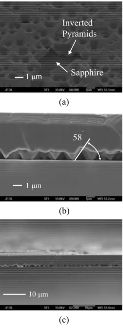
The material epitaxial growth uses nominal low pressure metalorganic chemical vapor deposition共MOCVD兲. A 30 nm of low temperature GaN nucleation layer followed by a 2.5 m GaN buffer layer was grown on 共0001兲 sapphire template. The GaN wafer was immersed in high temperature molten KOH at 280 ° C for 12 min. The molten KOH selec-tively etched defects on wafer surface and etched continu-ously downward opening up channels to sapphire interface. The molten KOH was led to GaN-sapphire interface through these self-assembled channel openings. The etching process then turned into lateral direction because the defect density was high at interface and etched away a thin layer of GaN along sapphire interface. It is known that KOH etching is typically anisotropic and preferentially etches specific crys-tallographic planes. A tilted view scanning electron micros-copy共SEM兲 image is shown in Fig.1共a兲, where the inverted pyramid structure at GaN-sapphire interface can be seen from a large opening. A large number of hexagonal pits were also formed on the surface. The etch pit density was ⬃5 ⫻108 cm−2 from SEM image estimation. Additional GaN was grown on the etched GaN wafer to fill up both the etched openings and surface pits to provide flat top surface for the subsequent LED device growth. The LED device structure was 3.5 m n-doped GaN, ten pairs of Al0.05Ga0.95N/InGaN quantum wells 共13/2.5 nm兲, and 100 nm of p-doped GaN cap layer. The designed emission wave-length is at 395 nm. A cross-sectional SEM image of a cleaved sample after regrowth process is shown in Fig.1共b兲. The space and the inverted pyramid structures created at the GaN-sapphire interface are still well maintained and distrib-uted throughout the large area, as shown in the zoom out Fig.
1共c兲. Most of the pyramid tips are still in contact with sap-phire. To investigate the performance of the device structure and make fair comparisons, a reference wafer also went through exactly the same fabrication process except for skip-ping the KOH etching step.
a兲Electronic mail: [email protected].
APPLIED PHYSICS LETTERS 95, 041109共2009兲
0003-6951/2009/95共4兲/041109/3/$25.00 95, 041109-1 © 2009 American Institute of Physics
This article is copyrighted as indicated in the article. Reuse of AIP content is subject to the terms at: http://scitation.aip.org/termsconditions. Downloaded to IP: 140.113.38.11 On: Wed, 30 Apr 2014 14:58:28
The x-ray diffraction共XRD兲 rocking curves of these two samples are shown in Fig.2. The linewidth for共102兲 planes was reduced from 552 to 472 arc sec. The linewidth for 共002兲 planes was only reduced from 338 to 335 arc sec.
The XRD linewidths for 共102兲 and 共002兲 planes are related to edge and screw threading dislocation densities, respectively.11The decrease in XRD linewidth indicates im-proved material quality. The improvement is attributed to the strain relaxation of the partially relieved GaN layer by inter-facial etching and the subsequent regrowth. When GaN epi-taxial layer was first grown on sapphire, a compressive strain was built up in the material due to the mismatched lattice constants and thermal expansion coefficients between GaN and sapphire. The KOH interfacial etching partially relieved GaN from sapphire interface and relaxed the compressive strain. This partially relieved layer served as a buffer layer to reduce the problems of mismatched lattice constants and thermal expansion coefficients during MOCVD regrowth and led to improved crystal quality.
These two samples were made into LED chips. Indium tin oxide was used as a current spreading layer and Ni/Au as a p-type electrode contact. Ti/Al/Ni/Au was deposited on the exposed n-GaN to serve as an n-type electrode contact. The sapphire substrates of both samples were lapped down and a 240 nm Al metal reflector coating was deposited on the sap-phire back surface. The use of back reflector is common in finished LED package. Therefore, it was also included. They were finally scribed into 350⫻350 m2 LED chips. The schematic of the LED with inverted micropyramid structures 共IP-LED兲 is shown in Fig.3共a兲. The reference LED共R-LED兲 has similar structure except for a flat GaN-sapphire interface. The electroluminescence 共EL兲 spectra of both LEDs col-lected in the normal to the front surface direction are shown in Fig. 3共b兲. The peak intensity of IP-LED is enhanced by 112% compared to that of R-LED. The EL spectrum of R-LED shows slight Fabry–Pérot mode ripples. The Fabry– Pérot mode spacing is about 5 nm, which is consistent with the overall GaN thickness of 6 m and refractive index of ⬃2.55 at 394 nm. The EL spectrum of IP-LED on the other hand does not have the same Fabry–Pérot mode ripples. This is because the randomly distributed micropyramid structures suppress the standing wave formation between the top and bottom interfaces. The peak wavelength of IP-LED is red-shifted by ⬃2 nm compared to that of R-LED, indicating the relaxation of compressive strain in IP-LED.12
The light-current共L-I兲 and voltage-current 共V-I兲 charac-teristics are shown in Fig. 3共c兲. The forward voltages of
IP-Sapphire
Inverted
Pyramids
1 μmSapphire
Inverted
Pyramids
1 μm(a)
58
∘ 1 μm58
∘58
∘ 1 μm(b)
10 μm 10 μm(c)
FIG. 1.共a兲 SEM image of the etched GaN surface. 共b兲 SEM cross-sectional
image of the regrown sample.共c兲 A zoom out view of the inverted pyramid
structures.
FIG. 2. 共Color online兲 XRD rocking curves for IP-LED and R-LED
samples. u-GaN MQWs Al mirror Sapphire u-GaN ITO p-GaN n-GaN Al mirror u-GaN MQWs Al mirror Sapphire u-GaN ITO p-GaN n-GaN Al mirror (a) (b) (c) (d)
FIG. 3.共Color online兲 共a兲 Schematic of IP-LED structure. 共b兲 EL spectra of
IP-LED and R-LED in normal direction.共c兲 L-I-V curves of IP-LED and
R-LED.共d兲 Far field patterns of IP-LED and R-LED.
041109-2 Lo et al. Appl. Phys. Lett. 95, 041109共2009兲
This article is copyrighted as indicated in the article. Reuse of AIP content is subject to the terms at: http://scitation.aip.org/termsconditions. Downloaded to IP: 140.113.38.11 On: Wed, 30 Apr 2014 14:58:28
LED and R-LED are 3.86 and 3.80 V, respectively, at 20 mA and increase to 5.09 and 4.93 V at 100 mA. The electric characteristic of IP-LED is still reasonably well maintained. The optical power of IP-LED and R-LED collected by an integrating sphere are 7.31 and 3.95 mW at 20 mA and 37.5 and 23.7 mW at 100 mA, respectively. The IP-LED output power exhibits 85% and 58% enhancement at 20 and 100 mA, respectively. The decrease of output power enhance-ment is likely due to the lower thermal conductance from the smaller GaN-sapphire contacts. The small interface contacts on the other hand are crucial for relieving the compressive strain and reducing material defects as described previously, which in turn reduces heat generation. The low thermal con-ductance problem is therefore not as serious as it would be. We also measured the far field pattern at 20 mA injection current as shown in Fig. 3共d兲. The IP-LED emission in nor-mal direction is much more enhanced. The emission intensity is enhanced by 120% in normal direction and 62% in 45° direction. The divergent angles of IP-LED and R-LED are 108° and 128°, respectively.
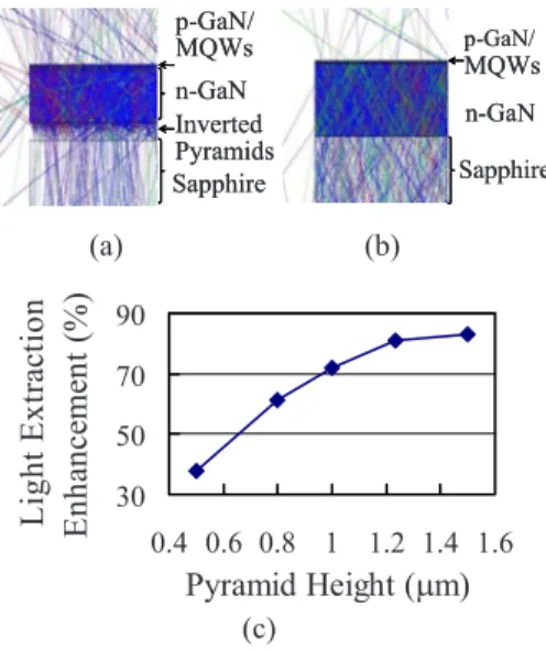
To obtain a better physical understanding of output power improvement, ray tracing simulations based on Monte Carlo method are carried out for both LEDs. There is a slight distribution of pyramid heights. The pyramid facet angle is however fairly well defined as can be seen from Fig.1共b兲. To simplify the calculation, an averaged pyramid height of 1 m and 58° facet angle were used. This model is not exact but is believed to be close enough to provide reasonable estimates. Figures4共a兲and4共b兲are the ray tracing results for
both LEDs. The inverted pyramid structures indeed effec-tively increase light output in the front surface direction. The light extraction efficiencies versus various pyramid heights are also calculated, as shown in Fig. 4共c兲. The calculated 72% enhancement at 1 m pyramid height accounts for the major part of the observed 85% total power enhancement. The other 13% enhancement can be attributed to internal quantum efficiency improvement from better crystal quality. The simulation also shows that light extraction enhancement for 1 m pyramid height is close to the optimum enhance-ment value.
In conclusion, we have demonstrated a high efficiency UV LED with inverted micropyramid structures at GaN-sapphire interface. The micropyramid structures were created by interfacial anisotropic chemical wet etching without the use of photolithography patterning. The LED was fabricated by growth interrupt, chemical etching, and regrowth pro-cesses. The device electrical performance is well maintained after these steps. The overall optical output power has shown significant 85% enhancement at nominal operating current 20 mA, which is attributed to both improved crystal quality and better light extraction efficiency.
This work was financially supported by the MOE ATU program and in part by the National Science Council of Republic of China 共ROC兲 Taiwan under Contract Nos. NSC97-2120-M-009-001, NSC95-3114-P-009-001-MY2, and NSC97-2112-M-00兴27-MY3 and by the Sinica Nano-program.
1T. Fujii, Y. Gao, R. Sharma, E. L. Hu, S. P. DenBaars, and S. Nakamura,
Appl. Phys. Lett. 84, 855共2004兲.
2C.-E. Lee, Y.-C. Lee, H.-C. Kuo, T.-C. Lu, and S.-C. Wang,IEEE
Photo-nics Technol. Lett. 20, 659共2008兲.
3S. J. Chang, C. F. Shen, W. S. Chen, C. T. Kuo, T. K. Ko, S. C. Shei, and
J. K. Sheu,Appl. Phys. Lett. 91, 013504共2007兲.
4A. David, T. Fujii, E. Matioli, R. Sharma, S. Nakamura, S. P. DenBaars,
and C. Weisbuch,Appl. Phys. Lett. 88, 133514共2006兲.
5T. A. Truong, L. M. Campos, E. Matioli, I. Meinel, C. J. Hawker, C.
Weisbuch, and P. M. Petroff,Appl. Phys. Lett. 94, 023101共2009兲.
6Y. J. Lee, H. C. Kuo, T. C. Lu, B. J. Su, and S. C. Wang,J. Electrochem.
Soc. 153, G1106共2006兲.
7A. Bell, R. Liu, F. A. Ponce, H. Amano, I. Akasaki, and D. Cherns,Appl.
Phys. Lett. 82, 349共2003兲.
8J. Lee, S. Ahn, S. Kim, D.-U. Kim, H. Jeon, S.-J. Lee, and J. H. Baek,
Appl. Phys. Lett. 94, 101105共2009兲.
9K. Tadatomo, H. Okagawa, Y. Ohuchi, T. Tsunekawa, Y. Imada, M. Kato,
and T. Taguchi,Jpn. J. Appl. Phys., Part 2 40, L583共2001兲.
10E.-H. Park, J. Jang, S. Gupta, I. Ferguson, C.-H. Kim, S.-K. Jeon, and J.-S.
Park,Appl. Phys. Lett. 93, 191103共2008兲.
11H. Heinke, V. Kirchner, S. Einfeldt, and D. Hommel,Appl. Phys. Lett.77,
2145共2000兲.
12P. P. Paskov, R. Schifano, T. Malinauskas, T. Paskova, J. P. Bergman, B.
Monemar, S. Figge, D. Hommel, B. A. Haskell, P. T. Fini, J. S. Speck, and
S. Nakamura,Phys. Status Solidi C 3, 1499共2006兲.
p-GaN/ MQWs n-GaN Sapphire Inverted Pyramids p-GaN/ MQWs n-GaN Sapphire Inverted Pyramids Sapphire n-GaN p-GaN/ MQWs Sapphire n-GaN p-GaN/ MQWs (a) (b) 30 50 70 90 0.4 0.6 0.8 1 1.2 1.4 1.6 Pyramid Height (μm) Light Extr ac tion Enha nc em en t (%) (c)
FIG. 4. 共Color online兲 Monte Carlo ray tracing simulations. 共a兲 and 共b兲 are
zoom in views at GaN-sapphire interface for IP-LED and R-LED.共c兲 Light
extraction enhancements vs different pyramid heights.
041109-3 Lo et al. Appl. Phys. Lett. 95, 041109共2009兲
This article is copyrighted as indicated in the article. Reuse of AIP content is subject to the terms at: http://scitation.aip.org/termsconditions. Downloaded to IP: 140.113.38.11 On: Wed, 30 Apr 2014 14:58:28