2008 June • JOM www.tms.org/jom.html 77 Overview lead-Free solder
the Effect of pre-aging on the
Electromigration of Flip-chip snag
solder Joints
Po-Chun Yang, Chien-Chih Kuo, and Chih Chen
How would you…
…describe the overall signifi cance of this paper?
Pre-aging at 170°C was able to increase the electromigration lifetime of fl ip-chip solder joints, which has not been reported previously.
…describe this work to a materials science and engineering professional with no experience in your technical specialty?
The effect of pre-aging on electromigration is investigated in this study of fl ip-chip SnAg solder joints. It was found that the average failure time increased about three times when the joints were pre-aged at 170°C for 3 to 25 hours. …describe this work to a layperson?
In high-performance devices such as microprocessors, there are thousands of solder bumps in one chip. It was found that the lifetime of the devices may increase three times when the devices are heated to 170°C for 3 to 25 hours prior to usage of the devices.
The effect of pre-aging on electromi-gration is investigated in this study us-ing fl ip-chip SnAg solder joints. The solder joints were pre-aged at 170°C for 1 h, 3 h, 5 h, 10 h, 25 h, and 50 h, and then they were subjected to electro-migration tests of 0.9 A at 150°C. It was found that the average failure time increased about three times when the joints were pre-aged for 3 h to 25 h. But it decreased when the joints were over-aged. It is proposed that the major con-tributor to the prolonged failure time may be the densifi cation of the nickel and copper under-bump metallization (UBM) and the solder due to the aging treatment. The pre-aging treatment at 170°C may stabilize the microstructure of the solder. The vacancies in the sol-der were annihilated during the heat treatment, causing a slower diffusion rate. In addition, the UBM structure became denser after the pre-aging pro-cess. Thus, the denser UBM structure may lead to slower consumption rates of the nickel and copper layers, result-ing in the enhancement of electromi-gration resistance.
introduction
The fl ip-chip solder joint has become the most important technology for high-density packaging in the microelec-tronic industry.1 As the required perfor-mance in microelectronics devices be-comes higher, thousands of solder bumps are fabricated into one chip. Thus the size of the joints progressively shrinks, with a diameter of about 100 µm or less. The design rule of packaging requires that each bump is going to carry 0.2 A to 0.4 A, resulting in a current density of approximately 2 × 10³ A/cm2 to 2 × 10⁴ A/cm2. There-fore, electromigration has become an important reliability issue for fl ip-chip
solder joints.2
The previous studies on electromi-gration of fl ip-chip solder bumps were mainly focused on eutectic SnPb sol-ders.3–5 Current crowding effect on the cathode/chip side was proposed to be responsible for the failure at the cath-ode/chip side of the SnPb bumps.1,6 Three-dimensional simulation has been carried out to depict the current density distribution in solder bumps and a hot spot was proposed to occur at the re-gion of current crowding.7,8 The current crowding induced by electromigration still plays a crucial role in the failure of the bumps. Recently, due to environ-mental concerns, studies have been conducted on the electromigration of
lead-free solder bumps.9–11 Particularly, several approaches have been proposed to relieve the current crowding and Joule heating effect in the joints, hop-ing to prolong the electromigration life-time of the joints. The approaches mainly include enlarging the cross sec-tion for aluminum traces in the chip end12 and using thicker under-bump metallizations (UBMs).13–15 It is report-ed that thicker UBMs keep the solder away from current-crowded and hot-spot regions and thus may increase the electromigration resistance.3,14 Solid-state aging may form thicker interme-tallic compound (IMC) layers and this may be able to increase the electromi-gration resistance. However, the effect of pre-aging on the electromigration of fl ip-chip solder joints is not clear. In this paper, lead-free eutectic SnAg solder joints were annealed at various conditions to produce various thick-nesses of Ni3Sn4 IMCs. Then electro-migration tests were performed on the joints to examine the effect of the pre-aging on failure time and failure mech-anism. It was found that the appropriate amount of pre-aging at 170°C may in-crease the electromigration resistance. See the sidebar for experimental de-tails.
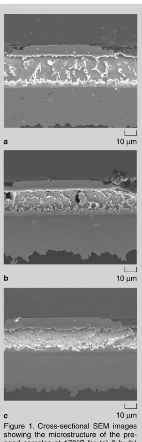
rEsults and discussion By controlling the annealing condi-tions, solder bumps with various IMC thicknesses can be fabricated. Since electromigration failure occurs in the chip side of the solder joints, the thick-ness of the Ni3Sn4 layer on the substrate end will not be discussed in this paper. The Ni3Sn4 layer was 1.96 µm on the chip side before aging. Figure 1a through c show the cross-sectional SEM images for the solder bumps after the solid-state aging at 170°C for 0 h,
JOM • June 2008
78 www.tms.org/jom.html
5 h, and 50 h. The solders were selec-tively etched to reveal the morphology of the IMC layers. The IMC was identi-fied as Ni3Sn4 for all the samples used in this study using scanning-electron microscopy–energy dispersive spec-troscopy (SEM-EDS). The thickness was 1.96 µm, 2.15 µm, and 3.27 µm for the three samples, respectively. The Ni3Sn4 thicknesses for all the annealing conditions are shown in Figure 2. The Ni3Sn4 IMC layer on the chip end grew thicker as the aging time increased. At the same time, some of the nickel layer was consumed due to the IMC forma-tion. Yet, the copper UBM remained
in-tact after all the annealing conditions. To investigate how the pre-aging af-fects electromigration failure time, the joints were stressed by 0.9 A at 150°C. The failure criteria was defined when the bump resistance of Bump 3 in-creased 20% of its original value. The mean failure time was obtained by av-eraging the results of three samples for all the annealing conditions. Figure 3 shows the average failure time as a function of the pre-aging time. The fail-ure time without pre-aging treatment was 103 h, and increased significantly after the aging treatment. With pre-aging of 1 h, the failure time increased to 173 h, and it further increased to 325 h for the samples pre-aged for 3 h. The slight drop in failure time for the samples pre-aged for 5 h may be attrib-uted to sample variation. It reaches a peak value of 331 h for the samples pre-aged for 25 h. The results indicate that the failure time can be prolonged by ap-proximately three times by a simple pre-aging treatment at 170°C for few hours to 25 h. Yet, it decreases to 238 h for the samples pre-aged for 50 h.
The failure mechanism was exam-ined to investigate the reasons for this interesting observation. Figure 4a through c presents the cross-sectional SEM images on the failure site for the bumps with pre-aging for 0 h, 5 h, and 50 h, respectively. The electron flow entered from the aluminum trace on the left-hand side, as indicated by the ar-rows. Dissolution of the nickel UBM was observed on the failure sites. Once the nickel UBM was destroyed, the 5 µm copper UBM dissolved quickly into the solder to form (Cu, Ni)6Sn5 ter-nary IMCs. Since copper atoms were migrated into the solder by the electron flow, voids accumulated in the contact opening. Both the IMCs and void for-mations are responsible for the increase in bump resistance.
It is speculated that a thicker Ni3Sn4 layer may relieve the current-crowding effect in the flip-chip solder joints. A three-dimensional (3-D) finite-element method was employed to simulate the current-density distributions in the
sol-Figure 1. Cross-sectional SEM images showing the microstructure of the pre-aged samples at 170°C for (a) 0 h; (b) 5 h; and (c) 50 h. The sample thickness is 1.96 µm, 2.15 µm, and 3.27 µm, respectively. 10 µm 10 µm 10 µm a b c
Figure 3. Average electromigration failure time of solder joints as a function of pre-aging time. The failure time increases rapidly with proper pre-aging time. Yet, it decreases for the bumps after the aging for 50 h.
Figure 2. The measured thickness of the Ni3Sn4 IMC layer on the chip end as a function of pre-aging time at 170°C. The IMC grew thicker as the annealing time increases.
10 µm c
Figure 4. Cross-sectional SEM images showing the microstructure on the failure sites for the samples pre-aged at 170°C for (a) 0 h; (b) 5 h; and (c) 50 h. Dissolution of the nickel and copper UBM was responsible for the electromigration failure.
10 µm b
10 µm a
2008 June • JOM www.tms.org/jom.html 79 ExpErimEntal procEdurEs
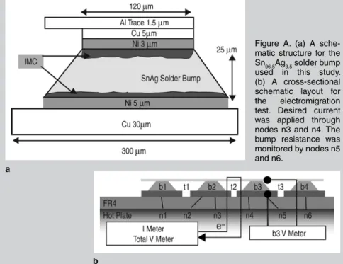
The dimensions of the flip-chip joints used in this study are shown schematically in Figure Aa. The Sn96.5Ag3.5 bump has a dimension of 130 µm in width and about 25 µm in height with an under-bump metallization (UBM) opening of 120 µm in diameter. The solder joints consist of eutectic SnAg solder bumps with an electroplated 5 µm-Cu/elec-troplated 3 µm-Ni UBM. The four bumps are connected together with aluminum trace 2,550 µm long, 100 µm wide, and 1.5 µm thick. The bumps were annealed at 170°C for various durations of time, including 1 h, 3 h, 5 h, 10 h, 25 h, and 50 h.
Kelvin bump probes were adopted to measure the resistance changes during electro-migration and they consist of four bumps, which are denoted as bump 1 through bump 4, as shown in Figure Ab. Six copper nodes were fabricated on the substrate side and they are labeled as Nodes n1 though n6. The copper lines on FR5 substrates were 25 µm thick and 100 µm wide. Bump 2 and bump 3 were applied by 0.9 A current at 150°, in which the electron flow goes from the board side to the chip side in bump 2, whereas it is from the chip side to the board side for bump 3. Kelvin probes were employed to moni-tor the resistance changes for both bumps 2 and 3.16 Thus the degree of damage can be
measured for these two bumps. In this study, we define the electromigration failure as the resistance of the bump 3 increases 20% of its original value. Field-emission scanning-electron microscopy of JEOL 6500 was employed to observe surface microstructure, and energy-dispersive spectroscopy was used to analyze compositions.
Table I. The Resistivity of the Materials used in the Simulation Models
Resistivity at 20°C Materials (µΩ-cm) Al Trace 3.2 Electroless Ni 70.0 Cu 1.7 Ni 6.2 SnAg Solder 11.5 Ni3Sn4 28.5
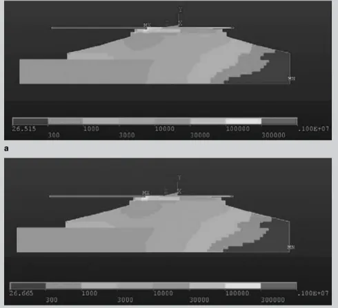
der joints with the pre-aging for 0 h and 25 h. The dimensions of the two mod-els were identical except the thickness of the IMCs and the remaining nickel layer in the chip and in the substrate ends. The Ni3Sn4 layer on the chip side was 1.96 µm and 2.57 µm for the solder bumps with pre-aging for 0 h and 25 h, respectively. The consumption of the nickel UBM was also considered. Layered-type Ni3Sn4 IMCs were used in this simulation to avoid difficulty in meshing. The parameters of the materi-als used in the simulation were tabu-lated in Table I. The model used was SOLID69 8-node hexahedral coupled field element using ANSYS simulation software developed by ANSYS Inc. It is surprising that the simulation re-sults indicate that no obvious differ-ences in current density distribution were observed between the two bumps, as presented in Figure 5a and b. Yet, the bump with the pre-aging for 25 h has a slightly lower maximum current densi-ty. The value is 21,923 A/cm2, which is only about 0.4% lower than that of the bump without the pre-aging treatment. The difference in failure time could be estimated using the mean-time-to-fail-ure equation for solder joints, which is typically expressed as17
where A is a constant, j is the current density in amperes per centimeter square, n is a model parameter for cur-rent density, Q is the activation energy, k is Boltzmann’s constant, and T is the average bump temperature in degrees Kelvin. To estimate the failure time dif-ference due to the variation of current density distribution, the maximum cur-rent density and the stressing tempera-ture were adopted for the values of j and T, respectively. In addition, the
val-ues of n and Q used are adopted as 0.678 eV and 0.691 eV, respectively.18 The calculation results indicate that the thicker Ni3Sn4 layer can only prolong the failure time less than 1%. Yet, the experimental data show that the mean failure time for the bumps with the pre-aging for 25 h is about 3.2 times that of the non-aged one. Thus, the major rea-son for the higher electromigration re-sistance does not come from the change in current density distribution due to the IMC formation.
The major contributor to the pro-longed failure time after the proper
ag-ing conditions may come from the den-sification of the UBM and the solder. C.Y. Liu et al. performed electromigra-tion tests in thin solder strips and they found that the electromigration rate of pure tin could be reduced by about 50% when the strips were annealed at 150°C for 48 h.19 The annealing temperature in this study is 170°C, which is higher than 150°C. Therefore, it is speculated that the pre-aging treatment at 170°C may stabilize the microstructure of the solder. The vacancies in the solder were annihilated during the heat treatment, causing a slower diffusion rate. In
addi-b a
Figure A. (a) A sche-matic structure for the Sn96.5Ag3.5 solder bump used in this study. (b) A cross-sectional schematic layout for the electromigration test. Desired current was applied through nodes n3 and n4. The bump resistance was monitored by nodes n5 and n6. MTTF A j Q kT n = 1 exp
tion, the UBM structure became denser after the pre-aging process. As men-tioned previously, the consumption of the nickel layer plays a crucial role in the electromigration failure. The denser UBM structure may lead to slower con-sumption rates of the nickel and the copper layers. Thus, proper annealing treatment is able to enhance electromi-gration resistance by about three
times.
On the other hand, over-aging may consume too much of the nickel UBM and result in a shorter failure time. For the solder bump pre-aged for 50 h, as shown in Figure 1c, the remaining nickel UBM was about 2.1 µm after the annealing treatment. Since the nickel layer serves as a diffusion barrier for the copper UBM, the electromigration
lifetime may decrease when the nickel UBM becomes too thin. Therefore, the average failure time dropped to 238 h for the solder bumps pre-aged for 50 h. references
1. K.N. Tu, J. Appl. Phys., 94 (2003), p. 5451. 2. Chih Chen and S.W. Liang, J. Mater. Sci.: Materials in Electronics, 18 (2007), p. 259.
3. C.Y. Liu et al., Appl. Phys. Lett., 75 (1999), p. 58. 4. Y.H. Lin et al., Acta Mater., 53 (2005), p. 2029. 5. Hua Ye, Cemal Basaran, and Douglas Hopkins, Appl. Phys. Lett., 82 (2003), p. 7.
6. T.L. Shao et al., J. Appl. Phys., 98 (2005), p. 044509.
7. S.W. Liang, Y.W. Chang, and Chih Chen, Appl. Phys. Lett., 88 (2006), p. 022110.
8. S.H. Chiu et al., Appl. Phys. Lett., 88 (2006), p. 022110.
9. W.J. Choi, E.C.C. Yeh, and K.N. Tu, J. Appl. Phys., 94 (2003), p. 5665.
10. T.L. Shao et al., Journal of Applied Physics, 96 (8) (2004), p. 4518.
11. Y.H. Chen et al., J. Mater. Res., 20 (9) (2005), p. 2432.
12. S.W. Liang, Y.W. Chang, and Chih Chen, Appl. Phys. Lett., 88 (2006), p. 172108.
13. J.W. Nah et al., J. Appl. Phys., 100 (2006), p. 123513.
14. S.W. Liang, Y.W. Chang, and Chih Chen, J. of Electron. Mater., 36 (10) (2007), p. 1348.
15. S.W. Liang, Y.W. Chang, and Chih Chen, J. of Electron. Mater., 36 (2) (2007), p. 159.
16. Y.W. Chang, S.W. Liang, and Chih Chen, Appl. Phys. Lett., 89 (3) (2006), p. 032103.
17. J.R. Black, IEEE Trans. Electron Devices, ED-16 (4) (1969), p. 338.
18. Y.-S. Lai et al., Proceedings of 7th Electronic Packaging Technology Conference (Piscataway, NJ: IEEE Components, Packaging, and Manufacturing Technology Society, 2005), p. 786.
19. C.Y. Liu, Chih Chen, and K.N. Tu, J. Appl. Phys., 88 (2000), p. 5703.
Po-Chun Yang is a corporal with the military police of Taiwan, Chien-Chih Kuo is a master student and Chih Chen is a professor in the Department of Materials Science and Engineering at National Chiao Tung University, Hsin-chu 30010, Taiwan, Republic of China. Dr. Chen can be reached at [email protected].
Figure 5. Simulation results showing the current-density distributions for the solder bumps pre-aged at 170°C for (a) 0 h and (b) 25 h. No obvious difference in current distribution was found due to the variation in the thickness of the nickel and the IMC layers.
b a