Investigation of emission polarization and strain in InGaN/GaN
multiple quantum wells on nanorod epitaxially lateral overgrowth
templates
Huei-Min Huang, Tien-Chang Lu*, Chiao-Yun Chang, Yu-Pin Lan, Shih-Chun Ling, Wei-Wen
Chan, Hao-Chung Kuo, and Shing-Chung Wang
Department of Photonics & Institute of Electro-Optical Engineering, National Chiao Tung
University, Hsinchu 300, Taiwan
*E-mail address: [email protected].
ABSTRACT
Non-polar (a-plane) InGaN/GaN multiple quantum wells (MQWs) on the GaN nanorod epitaxially lateral overgrowth templates with different nanorod height have been fabricated. The average in-plane strain in the InGaN MQWs has been determined from 2.73×10⁻² to 2.58×10⁻² while the nanorod height in templates increases from 0 to 1.7 μm. The
polarization ratio of the emission from InGaN MQWs varies from 85 % to 53 % along with the increase of the GaN nanorod height. The reduction of polarization ratio has been attributed to the partial strain relaxation within the epitaxial structures as a result of growth on the GaN nanorod templates and the micro-size air-voids observed in the nanorod templates.
Keywords: Non-polar, InGaN/GaN MQWs, optical polarization, strain
1. INTRODUCTION
Conventional c-plane InGaN/GaN multiple quantum wells (MQWs) structure suffers from the quantum confinement stark effect (QCSE) due to the existence of spontaneous and piezoelectric polarization fields, leading to spatial separation of the electron and hole wave functions and to reduce the electron-hole recombination rate [1]. Growth along the non-polar [2], [3] and semi-polar [4], [5] oriented direction has been proved to be an effective approach to ease or eliminate the influence of polarization field in nitride-based materials. On the other hand, if growth direction rotates from c-plane to the non-polar orientation, the in-plane biaxial strain will change from isotropic to anisotropic situation. Due to the anisotropic in-plane strain in the non-polar (In, Ga)N material system, the original |X ± iY > valence band states are not degenerate any more [6]. |Z >-like and |Y >-like states will split larger to enhance the polarization ratio of light. The |Z >-like state transition is expected to be z-polarized light (ε//c), similarly the |Y>-like state transition is expected to be y-polarized light (ε⊥c). The strong y-polarized light emission, resulted from the different energy state transitions, can be measured.
Under the influence of the strong in-plane strain, the valence-band states will separate large enough to raise the emission polarization ratio. Recently, an inherent polarized light for non-polar orientation (In, Ga)N material system have been discussed to apply in the display back-lighting system, which may potentially reduce the fabrication cost [7]. Some features in a-plane InGaN-based MQWs, such as the phase segregation within InGaN layers, carrier localization effect, have also been shown to influence the emission polarization discussed by the theoretical simulations and experimental measurements [8]-[10]. However, most of studies on optical polarization effects of InGaN-based MQWs were generally under the different indium composition or different well thickness conditions. In this study, we grew the a-plane InGaN/GaN MQWs on the high crystal quality GaN nanorod epitaxially lateral overgrowth templates. Under defined parameters (the identical indium composition and well thickness) of a-plane InGaN-based MQWs, the optical polarization properties grown on the different nanorod height templates with different strain-induced effects were investigated and compared with the as-grown MQWs structure.
Gallium Nitride Materials and Devices VII, edited by Jen-Inn Chyi, Yasushi Nanishi, Hadis Morkoç, Joachim Piprek, Euijoon Yoon, Proc. of SPIE Vol. 8262, 82621Y
© 2012 SPIE · CCC code: 0277-786X/12/$18 · doi: 10.1117/12.906635 Proc. of SPIE Vol. 8262 82621Y-1
2. EXPERIMENTS
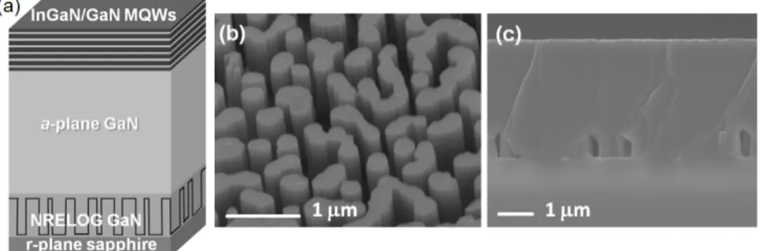
Fig. 1 (a) shows the sketch of the InGaN/GaN MQWs structure grown on a-plane GaN nanorod epitaxial lateral overgrowth templates. The detailed processes for a-plane GaN nanorod template have been described elsewhere [11]. The diameter of the nanorod is about 300−500 nm and the nanorod density is estimated to be around 6×10⁸/cm2
according to the scanning electron microscope (SEM) image shown in Fig. 1 (b). In order to understand the relationship between the optical polarization ratio from the MQWs structure and the nanorod height, the GaN nanorod height was varied from 0 μm, 0.2 μm, 0.7 μm, 1.2 μm, to 1.7 μm. All of the samples within this study possess the same MQWs structural parameters, consisting of 6 pairs of 7 nm In0.2Ga0.8N wells and 20 nm GaN barriers. The cross sectional SEM
image of the InGaN/GaN MQWs grown on GaN nanorod epitaxial lateral overgrowth templates exhibits a few micro-air-voids induced by the incomplete lateral overgrowth as shown in Fig. 1(c). For optical measurements, the polarization dependent photoluminescence (PL) was carried out at room temperature. The excitation source was a 325 nm He-Cd laser with an excitation power of 30 mW and the luminescence was collected using a polarizer in front of the spectrometer (Triax 320) with a photomultiplier tube (PMT) for ultraviolet-visible wavelengths. The light polarization is measured at the surface normal direction with a collection angle of 8 degrees. The linear polarizer for visible wavelength was set in front of the light collection fiber to examine the polarization property. The numerical aperture (N.A.) of the optical measurement system is about 0.15. In the case of the a-plane sample, a polarized angle of 0 degrees is defined to be parallel to the c-axis (ε//c) while the 90 degrees is along m-axis (ε⊥c). Raman spectroscopy was employed to determine the strain variation in the MQWs structure grown on the different GaN nanorod template. The dispersed Raman spectra were detected by a focal length 500 mm spectrograph (Acton SP 2500) with the 1800 grooves/mm grating, and the spectral resolution of around 1 cm-1 was achieved at the exciting source of 532 nm.
Fig. 1. (a) The sketch of a-plane InGaN/GaN MQWs structure grown on GaN nanorod templates. (b) The SEM image of the GaN nanorod template fabricated by self-assembled Ni nanomasks and coupled plasma reactive-ion etching. (c) The cross-sectional SEM image of InGaN/GaN MQWs grown on the GaN nanorod epitaxially lateral overgrowth templates.
3. RESULTS AND DISCUSSION
In order to clarify the evolution of the polarization ratio and the energy peak ΔE difference in the GaN nanorod template with the different nanorod heights, the polarization dependent PL spectra for InGaN/GaN MQWs grown on the different GaN nanorod height in templates as 0 (as-grown), 0.2, 0.7, 1.2 and 1.7 μm have been carried out. It can be seen that the PL intensity increases with polarization angle from 0o (ε//c) to 90o (ε⊥c), implying that polarized light emitted from the
a-plane as-grown and the nanorod template samples. Figure 2 shows the integrated PL intensity with the different
polarization angles. The polarization ratio ρ is defined as (I⊥-I//)/( I⊥+I//) using the integrated PL intensity for two
orthogonal polarization directions, I⊥ and I//. The polarization ratio appears an obvious reduction for InGaN/GaN MQWs
grown on GaN nanorod template, and decreases from 85 % to 53 % with the increase of the GaN nanorod height. The polarization ratio seems to be influenced by using the nanorod template in contrast with the as-grown sample. The observable peak energy shift (ΔE) can be found between the emissions polarized to ε//c (0°) and to ε⊥c (90°), where ΔE is defined as (Eε//c-Eε⊥c). Compared with the nanorod epitaxial lateral overgrowth MQWs, the spectra for as-grown MQWs revealed a larger peak shift (about 32.1 meV).
Proc. of SPIE Vol. 8262 82621Y-2
Fig. 2. The integrated PL intensity of these two different MQWs samples at different polarization angles. The polarization-dependent PL spectra with the polarization angle ranging from 0° (c-axis [0001]) to 90° (m-axis [1100]) at room temperature for the a-plane InGaN/GaN MQWs grown on the 0 μm (as-grown) and 1.7 μm GaN nanorod template have been achieved.
Figure 3 summarized the polarization ratio (ρ) and the peak energy shift (ΔE) as a function of the GaN nanorod height in templates. Both the values of polarization ratio and the peak energy shift exhibit a decreasing tendency with increasing the GaN nanorod height in templates. It is well known that the non-polar InGaN/GaN MQWs structure suffers from anisotropic in-plane compressive strain, breaking the original valence band states. The peak energy shifts resulted from the splitting valence subbands could be raised with the increase of in-plane strain [12].Once the strain is decreased, subband splitting would be smaller and, in turn, lead to the reduction of the polarization ratio [13], [14].Thus we infer that the as-grown sample could be under the stronger in-plane strain; and the in-plane strain may be reduced with increasing the GaN nanorod height in templates.
Fig. 3. The polarization ratio (ρ) and the peak energy shift (ΔE) plotted as a function of the GaN nanorod height in templates.
Figure 4 (a) shows Raman spectra measured at room temperature, and the principal phonon modes are labeled at the corresponding peaks. E2(High) mode has the strongest intensity among all of the phonon modes. Since E2(High) mode is
an in-plane vibration mode and sensitive to strain, it is usually used to probe the in-plane strain. According to the Raman polarization selection rules, the A1(TO), E1(TO), and E2(High) modes can be observed by using the
x z y y
x( , + ) scattering configuration, where the assignments follow as x = a = [1120], y = m = 00][11 , and z = c = [0001]. In contrast with free standing a-plane GaN (568 cm-1) [15], the E
2(High) mode frequency shift is associated with
Proc. of SPIE Vol. 8262 82621Y-3
the induced compressive strain within a-plane GaN layers. The GaN template on the sapphire substrate is typically under compressive in-plane strain because of their differences in lattice mismatch and thermal expansion coefficient. Once compressive strain is introduced into GaN layer, the InGaN active layers are more strained by the virtue of heteroepitaxial growth on GaN layers [16]. The strain variation of InGaN active layers could be estimated via the analysis of E2(High) mode of GaN layers. The evolution of the phonon mode frequency as a function of the GaN
nanorod height in templates is shown in Fig. 4 (b). All phonon modes generated from GaN layer exhibit the red-shift trends with increasing the GaN nanorod height in templates. The frequency of E2(High) mode shifts slightly from 572 to
570 cm-1, that implied the in-plane strain was reduced after the GaN growth on nanorod templates. This strain reduction
could be partly attributed to the strain relaxation via the occurrence of the micro-air-voids in GaN nanorod epitaxially lateral overgrowth templates [Fig. 1(c)] [17].Besides,the evolution trend of in-plane strain measured by Raman spectra is consistent with the variation of polarization ratio shown in Fig. 3.
Fig. 4. (a) The room temperature Raman spectra of the InGaN/GaN MQWs grown on the GaN nanorod template with different nanorod height. (b) The frequency shift of the phonon modes as a function of the GaN nanorod height in templates.
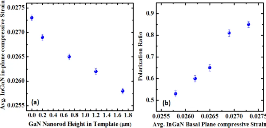
Fig. 5. (a) The values of the average in-plane strain of InGaN active layers plotted as a function of GaN nanorod height in templates. (b) The polarization ratio as a function of the average in-plane strain of InGaN active layers.
We employed the reference phonon mode frequency of 568 cm-1 and the linear proportionality factor of 2.7 cm-1·GPa-1
with the basal plane elastic modulus Cij to determine the in-plane biaxial strain further [15]. According to the strain evolution of GaN layers, the values of average in-plane strain in InGaN active layers were also calculated, and plotted as a function of the GaN nanorod height in Fig. 5(a). The average in-plane compressive strain of 3.11×10⁻³ (the stress of 1.5
GPa) in the as-grown sample have been obtained. When the variation of nanorod height reaches to 1.7 μm, the compressive strain almost reduces to half (about 1.53×10⁻³). An obvious reduction of the average in-plane compressive
Proc. of SPIE Vol. 8262 82621Y-4
strain of InGaN active layers can be observed, and it is decreased from 2.73×10⁻² to 2.58×10⁻² for the nanorod height
varying from 0 to 1.7 μm. Based on these experimental results, the variation of in-plane strain has been analyzed in our
a-plane InGaN/GaN MQWs samples grown on the GaN templates with different nanorod height. The strain relaxation in
the regrown layer including MQWs structure by using the nanorod template is believed to be one of the reasons for obtaining better crystal quality in terms of the narrow X-ray rocking curves [11]. Furthermore, the correlation between the average in-plane strain in the InGaN active layer and the polarization ratio is summarized, as shown in Fig. 5 (b). The polarization ratio depends on the variation of in-plane strain is obtained. It is believed that the decrease of the in-plane strain could diminish the valence subband splitting, leading to the reduction of the polarization ratio. On the other hand, when the GaN nanorod height in templates is increased, more micro-air-voids are observed inthe template. These micro-size air-voids would lead to the reduction of polarization ratio to a certain extent.
4. SUMMARY
In conclusion, a-plane InGaN/GaN MQWs structures grown on the GaN nanorod templates with different nanorod height have been investigated. We have demonstrated that the growth on nanorod templates can reduce the in-plane compressive strain within the samples in comparison to the as-grown sample by performing the polarization-dependent PL and Raman scattering spectra, respectively. The polarization-dependent PL reveals that the polarization ratio decreases with increasing the GaN nanorod height in templates due to the reduction of strain and appearance of micro-size air-voids.
5. ACKNOWLEDGEMENT
These works were supported by the MOE ATU program and in part by the National Science Council of Republic of China (ROC) in Taiwan under contract No NSC-98-3114-M-009-001 and NSC-99-2120-M-009-007.
6. REFERENCES
[1] P. Waltereit, O. Brandt, A. Trampert, H. T. Grahn, J. Menniger, M. Ramsteiner, M. Reiche, and K. H. Ploog, “Nitride semiconductors free of electrostatic fields for efficient white light-emitting diodes,” Nature, vol. 406, pp. 865, (2000).
[2] P. Waltereit, O. Brandt, M. Ramsteiner, A. Trampert, H. T. Grahn, J. Menniger, M. Reiche, R. Uecker, P. Reiche, and K. H. Ploog, “Growth of M-Plane GaN (1-100): A Way to Evade Electrical Polarization in Nitrides,” Phys. stat. sol. (a), vol. 180, pp. 133,( 2000).
[3] M. D. Craven, S. H. Lim, F. Wu, J. S. Speck, and S. P. DenBaars, “Structural characterization of nonpolar (11-20)
a-plane GaN thin films grown on (1-102) r-plane sapphire,” Appl. Phys. Lett., vol. 81, pp. 469, (2002).
[4] Chakraborty, T. J. Baker, B. A. Haskell, F. Wu, J. S. Speck, S. P. Denbaars, S. Nakamura, and U. K. Mishra, “Milliwatt Power Blue InGaN/GaN Light-Emitting Diodes on Semipolar GaN Templates,”Jan. J. Appl. Phys., vol. 44, L945, (2005).
[5] R. Sharma, P. M. Pattison, H. Masui, R. M. Farrell, T. J. Baker, B. A. Haskell, F. Wu, S. P. DenBaars, J. S. Speck, and S. Nakamura,” Demonstration of a semipolar (1013) InGaN/GaN green light emitting diode,” Appl. Phys. Lett., vol. 87, pp. 231110, (2005).
[6] S. Ghosh, P. Waltereit, O. Brandt, H. T. Grahn, and K. H. Ploog,“Electronic band structure of wurtzite GaN under biaxial strain in the M plane investigated with photoreflectance spectroscopy,” Phys. Rev. B, vol. 65, pp. 075202, (2002).
[7] H. Masui, H. Yamada, K.Iso, J. S. Speck, S. Nakamura, and S. P. DenBaars, “Optical polarization characteristics of m-oriented InGaN/GaN light-emitting diodes with various indium compositions in single-quantum-well structure,” J. Soc. Inf. Disp., vol. 16, pp. 571,(2008).
[8] N. A. EI-Masry, E. L. Piner, S. X. Liu, and S. M. Bedair, “Phase separation in InGaN grown by metalorganic chemical vapor deposition,” Appl. Phys. Lett., vol. 72, pp. 40, (1998).
[9] T. Koyama, T. Onuma, H. Masui, A. Chakraborty, B. A. Haskell, S. Keller, U. K. Mishra, J. S. Speck, S. Nakamura, S. P. DenBaars, and T. Sota, “Prospective emission efficiency and in-plane light polarization of nonpolar m-plane InxGa1−xN/GaN blue light emitting diodes fabricated on freestanding GaN substrates,” Appl. Phys. Lett., vol. 89, pp.
091906, (2006).
[10] C. H. Chiu, S. Y. Kuo, M. H. Lo, C. C. Ke, T. C. Wang, Y. T. Lee, H. C. Kuo, T. C. Lu, and S. C. Wang, “Optical properties of a-plane InGaN/GaN multiple quantum wells on r-plane sapphire substrates with different indium compositions,” J. Appl. Phys., vol. 105, pp. 063105, (2009).
[11] S. C. Ling, C. L. Chao, J. R. Chen, P. C. Liu, T. S. Ko, T. C. Lu, H. C. Kuo, S. C. Wang, S. J. Cheng, J. D. Tsay,
Proc. of SPIE Vol. 8262 82621Y-5
“Crystal quality improvement of a-plane GaN using epitaxial lateral overgrowth on nanorods,” J. Crys. Growth, vol. 312, pp. 1316, (2010).
[12] P. Misra, U Behn, O. Brandt, H. T. Grahn, B. Imer, S. Nakamura, S. P. DenBaars, and J. S. Speck, “Polarization anisotropy in GaN films for different nonpolar orientations studied by polarized photoreflectance spectroscopy,” Appl. Phys. Lett., vol. 88, pp. 161920, (2006).
[13] B. Liu, R. Zhang, Z. L. Xie, J. Y. Kong, J. Yao, Q. J. Liu, Z. Zhang, D. Y. Fu, X. Q. Xiu, P. Chen, P. Han, Y. Shi, Y. D. Zheng, S. M. Zhou, and G. Edwards, “Anisotropic crystallographic properties, strain, and their effects on band structure of m-plane GaN on LiAlO2(100),” Appl. Phys. Lett., vol. 92, pp. 261906, (2008).
[14] D. Fu, R. Zhang, B. Wang, Z. Zhang, B. Liu, Z. Xie, X. Q. Xiu, H. Lu, Y. D. Zheng, and G. Edwards, “Modification of the valence band structures of polar and nonpolar plane wurtzite-GaN by anisotropic strain,” J. Appl. Phys., vol. 106, pp. 023714, (2009).
[15] V.Y. Davydov, N.S. Averkiev, I.N. Goncharuk, D.K. Nelson, I.P. Nikitina, A.S. Polkovnikov, A.N. Smirnov, M.A. Jacobsen, O.K. Semchinova, “Raman and photoluminescence studies of biaxial strain in GaN epitaxial layers grown on 6H–SiC,” J. Appl. Phys., vol. 82, pp. 5097, (1997).
[16] H. Masui, S. Nakamura, S. P. DenBaars, and U. K. Mishra, “Nonpolar and Semipolar III-Nitride Light-Emitting Diodes: Achievements and Challenges,” IEEE Transactions on Electron Devices, vol. 57, issue 1, pp. 88-100, (2009).
[17] K. Y. Zang, Y. D. Wang, H. F. Liu, and S. J. Chua, “Structural and optical properties of InGaN/GaN multiple quantum wells grown on nano-air bridged GaN template,” Appl. Phys. Lett., vol. 89, pp. 171921, (2006).
Proc. of SPIE Vol. 8262 82621Y-6