IEEE MICROWAVE AND WIRELESS COMPONENTS LETTERS, VOL. 24, NO. 1, JANUARY 2014 11
Investigation of the Flip-Chip Package With BCB
Underfill for W-Band Applications
Chin-Te Wang, Li-Han Hsu, Wei-Cheng Wu, Heng-Tung Hsu, Senior Member, IEEE,
Edward Yi Chang, Senior Member, IEEE, Yin-Chu Hu, Ching-Ting Lee, Fellow, IEEE, and Szu-Ping Tsai
Abstract—Flip-chip package has great potential for use in
mil-limeter-wave applications. However, the coefficient of thermal ex-pansion mismatch between the chip and the substrate usually gen-erates thermal stresses that fracture the flip-chip structure. The use of underfills with low dielectric loss is essential to improve the mechanical strength and reliability of the flip-chip package. Benzo-cyclobutene (BCB) was used in this study as the underfill material for the flip-chip structure using the no-flow process. The flip-chip structure with BCB injection provides good RF performance with a return loss of better than 18 dB and an insertion loss of 0.6 dB up to 100 GHz, in addition to a lower dielectric loss. Furthermore, thermal cycle and shear force tests show that the underfill injection can significantly improve the reliability of a flip-chip package.
Index Terms—Benzocyclobutene (BCB), flip-chip packaging,
millimeter-wave, reliability, W-band.
I. INTRODUCTION
W
IRELESS communication and imaging systems at mil-limeter-wave and sub-milmil-limeter-wave frequencies are gaining increasing attention. Packages with good electrical per-formance, decent mechanical reliability and low cost are crucial for high frequency applications. Flip-chip interconnects are con-sidered to be a promising interconnect technology due to sev-eral reasons [1], [2]. Compared with conventional wire- bonding technology, flip-chip has much shorter interconnects, signifi-cantly reducing parasitic effects at millimeter-wave frequencies [3]. However, the reliability of flip-chip packaging is critical due to the thermal mechanical stresses from mismatch in the coef-ficient of thermal expansion (CTE) [4], [5]. Therefore, under-fill has been widely applied in the past. Many previous publica-tions have investigated the underfill effect in a flip-chip structure [6]–[8]. Low-noise amplifiers (LNA) flip-chip bonded Al O with an epoxy-based underfill was demonstrated in [6] with re-sponse shifted in frequency due to the underfill injection. In-crease in the fatigue life with only a small additional loss of flip-chip assemblies was presented in [5]. Improvement in theManuscript received June 10, 2013; revised August 20, 2013; accepted September 13, 2013. Date of publication November 14, 2013; date of current version January 06, 2014. This work was supported by the NCTU-UCB I-RiCE program, National Science Council of Taiwan under grant, NSC102-2911-I-009-302.
C.-T. Wang, L.-H. Hsu, W.-C. Wu, E. Y. Chang, Y.-C. Hu, and S.-P. Tsai are with the Department of Materials Science and Engineering, National Chiao Tung University, Hsinchu 300, Taiwan (e-mail: edc@mail.nctu.edu.tw).
H.-T. Hsu is with the Department of Communications Engineering and Com-munication Research Center, Yuan Ze University, Chunli 320, Taiwan.
C.-T. Lee is with the Department of Electrical Engineering, National Cheng Kung University, Tainan 701, Taiwan.
Color versions of one or more of the figures in this paper are available online at http://ieeexplore.ieee.org.
Digital Object Identifier 10.1109/LMWC.2013.2285213
TABLE I
MATERIALPROPERTIES OFUNDERFILLS
reliability with small loss of flip-chip structure on polymer sub-strate has also been achieved in [7].
Conventional epoxy-based underfill has a high dielectric loss tangent which induces extra signal dissipation and degrades RF performance. Previously, by performing the EM simulations, we demonstrated that the loss can be further reduced using lower loss underfill materials [8]. Therefore, the important considera-tions of underfill materials are low loss tangent, good thermo-mechanical properties and good process compatibility. Benzo-cyclobutene (BCB) is a good candidate as an underfill mate-rial. Table I summaries the material properties of conventional epoxy resin and BCB. BCB is designed for high frequency and low-k applications. It has been used for device passivation, in-terlayer dielectrics, and stress buffer layer. In general, BCB has a lower loss tangent than epoxy resin, making it very promising for millimeter-wave applications. The moisture uptake is also an important concern because moisture inside the materials can increase the dielectric loss at high frequencies [9], [10].
This study evaluates the feasibility of using BCB as an un-derfill material for flip-chip interconnects with applications up to W-band frequencies. In-house fabrication of the flip-chip in-terconnects and underfill material injection was performed and optimized. Reliability tests, including thermal cycle tests and shear force tests, were performed to verify the interconnect re-liability in flip-chip structures.
II. EXPERIMENT
In-house flip-chip interconnect structure with BCB underfill was performed in this study. The fabrication processes of the Gallium Arsenide (GaAs) thru-line chip and alumina (Al O ) substrate have been described in previous work [7]. Fig. 1(a) shows a schematic of the flip-chip structure. The total signal transmission path was 3 mm, including coplanar waveguide (CPW) on the Al O substrate, CPW on the GaAs chip, and two flip-chip transitions. An optimized no-flow underfill process, which will be described in the next section, was applied to fill BCB into the flip-chip structures. The characteristic impedance of the CPW transmission line on the GaAs chip and the Al O substrate was designed to be 50 . The underfill injection changes the effective dielectric constant and results in an impedance mismatch which degrades the chip
12 IEEE MICROWAVE AND WIRELESS COMPONENTS LETTERS, VOL. 24, NO. 1, JANUARY 2014
Fig. 1. (a) Schematic and (b) an SEM image of the cross section of the flip-chip structure with BCB underfill injection.
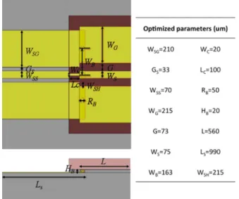
Fig. 2. Design parameters for the flip-chip structure with BCB injection.
performance. To reduce the impact of the underfill, the CPW transmission line on GaAs was designed to achieve an impen-dence matching of 50 . Compensation designs, such as ground pad shrinking and high impendence line, were also adopted on the substrate transmission line to compensate for the parasitic capacitance of the flip-chip interconnects, as shown in Fig. 2. After implementing matching designs, the RF performance has been evaluated and is shown in the next section.
Conventionally, a capillary underfill process is used to inject epoxy resin into the flip-chip structure. Unfortunately, liquid BCB cannot easily flow into the gap between the chip and sub-strate using capillary force. To solve this issue, the no-flow un-derfill process was proposed. Liquid BCB was first deposited on the substrate. Then the substrate was heated to cause BCB to flow. The heating conditions, such as the heating time and temperature, were optimized to enhance the BCB flow. Finally, the chip and the substrate were flip-chip bonded by using the Au-to-Au thermo-compression method. An additional curing at 250 C for 2 h was performed to facilitate cross-linking of the BCB polymer chains. Fig. 1(b) shows a cross-sectional SEM image of the flip-chip structure with BCB underfill. The BCB was successfully injected into the flip-chip interconnect struc-ture using the no-flow underfill process.
III. RESULTS ANDDISCUSSIONS
The losses in the flip-chip interconnects with underfill in-clude mismatch loss and real loss. Mismatch loss is mainly due to the dielectric constant change from the underfill. To reduce the impact from the underfill, the dimensions of the chip trans-mission line were modified, and compensation designs on the substrate transmission line were adopted. Fig. 3 shows compar-ison of the flip-chip interconnects with and without underfill.
Fig. 3. Measured S-parameters of the flip-chip interconnects without UF and with BCB or epoxy underfill injection.
The flip-chip with BCB has lower loss than the flip-chip with epoxy at high frequencies. The return and insertion losses of the flip-chip structure with BCB were better than 18 dB and 0.6 dB, respectively, from DC to 100 GHz. As for the case if flip-chip without underfill, an insertion loss of 0.66 dB was ob-served. The corresponding contribution to the overall insertion loss at 90 GHz were further extracted to be 0.14 dB from the CPW trace on GaAs substrate, 0.26 dB from CPW on Al O , and 0.26 dB from the transition. It is then concluded that the op-timized design can effectively reduce the mismatch loss.
The real loss includes metal loss , dielectric loss, and radiation loss. The radiation loss can be neglected because it is very small. The dielectric loss is composed of chip loss , substrate loss and underfill loss . After the under-fill injection, the extra dielectric loss induces and degrades the transmission properties. Hence, to investigate the influence of underfill injection, the loss factor is calculated using (1) [11]
(1) The underfill loss can be calculated by subtracting the loss of the flip-chip without UF from the loss of flip-chip with UF. The losses of chip, substrate, and metal in the flip-chip struc-ture are also extracted by EM simulation for comparison. Fig. 4 shows the comparison of the loss factors between the metal, chip, substrate, epoxy, and BCB. As can be seen, the major losses are metal loss and underfill loss. The epoxy loss is near the metal loss. The BCB loss is lower than epoxy loss. The flip-chip package with BCB shows a lower insertion loss of 0.11 dB/mm compared to the epoxy loss of 0.24 dB/mm at 100 GHz. These results demonstrate that underfill materials with lower dielectric loss tangents, such as BCB, can effectively reduce the RF loss of the flip-chip assembly caused by the underfill. Given that fact that the metal loss contributed the most to the total loss as shown in Fig. 4, it is worth mentioning that for silicon CMOS process where much narrower traces are encountered, the improvement in overall loss due to BCB might not be as pronounced since the metal loss are much higher for such cases.
The flip-chip interconnect structure with BCB underfill has demonstrated excellent RF performance as described in pre-vious section. However, reliability is also of great concern to the industry. Thermal property analysis was performed by thermal
WANG et al.: INVESTIGATION OF THE FLIP-CHIP PACKAGE WITH BCB UNDERFILL FOR W-BAND APPLICATIONS 13
Fig. 4. and of the flip-chip interconnect structure as extracted from EM simulation; the and as extracted from the measurement for comparison.
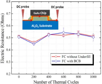
Fig. 5. Thermal cycling test results of the flip-chip interconnects with and without BCB underfill injection.
TABLE II SHEARFORCETESTRESULTS
cycling with temperature changes from C to 125 C with a dwell time of 15 min (the specifications of the JEDEC stan-dard) [12]. During the thermal cycling test, the DC resistance of the transmission line was measured after every 200 cycles, as shown in Fig. 5. The flip-chip structure with BCB passes a 1000 cycle thermal cycling test. The contact resistance showed little change and no samples failed after 1000 cycles. Table II shows the shear force test results before and after 1000 cycle thermal cycling tests. The results revealed that the flip-chip in-terconnects without underfill fractured at a shear force of 173 g which is not acceptable for commercial applications. After BCB injection, the shear force for failure was effectively increased to 1305 g. The shear force of the flip-chip structure degraded
after thermal cycling due to the thermal stresses induced by CTE mismatch. The flip-chip structure without underfill has a lower shear force resistance and the mechanical reliability was seri-ously degraded. However, the shear force resistance was en-hanced because the stress was redistributed by the underfill. BCB injection into flip-chip structures improves the reliability and excellent RF performance is retained after the packaging process.
IV. CONCLUSION
BCB was successfully injected into the flip-chip structures using the no-flow underfill process. The package with BCB un-derfill showed better RF performance with an insertion loss of better than 0.6 dB and a return loss of 18 dB up to 100 GHz, in addition to lower dielectric loss. Furthermore, thermal cy-cling and shear force testing showed that BCB injection could effectively improve the reliability of the flip-chip interconnect structure. Excellent RF performance with improved reliability demonstrates that BCB is a good underfill material for mil-limeter-wave package applications.
REFERENCES
[1] D. Staiculescu, J. Laskar, and E. M. Tentzeris, “Design rule devel-opment for microwave flip-chip applications,” IEEE Trans. Microw.
Theory Tech., vol. 48, no. 9, pp. 1476–1481, Sep. 2000.
[2] A. Jentzsch and W. Heinrich, “Theory and measurements of flip-chip interconnects for frequencies up to 100 GHz,” IEEE Trans. Microw.
Theory Tech., vol. 49, no. 5, pp. 871–878, May 2001.
[3] R. W. Jackson and R. Ito, “Modeling millimeter-wave IC behavior for flipped-chip mounting schemes,” IEEE Trans. Microw. Theory Tech., vol. 45, no. 10, pp. 1919–1925, Oct. 1997.
[4] Y. Ohshima, T. Nakazawa, K. Doi, H. Aoki, and Y. Hiruta, “Flip chip underfill reliability of CSP during IR reflow soldering,” in Proc. 35th
IEEE Int. Reliability Phys. Symp., Denver, CO, USA, Apr. 1997, pp.
124–128.
[5] Z. Feng, W. Zhang, B. Su, K. C. Gupta, and Y. C. Lee, “RF and me-chanical characterization of flip-chip interconnects in CPW circuits with underfill,” IEEE Trans. Microw. Theory Tech., vol. 46, no. 12, pp. 1823–1826, Jun. 1998.
[6] H. Kusamitsu, Y. Morishita, K. Maruhasi, M. Ito, and K. Ohata, “The flip-chip bump interconnection for millimeter-wave GaAs MMIC,”
IEEE Trans. Electron. Packag. Manufact., vol. 22, pp. 23–28, 1999.
[7] L.-H. Hsu, C.-W. Oh, W.-C. Wu, E. Y. Chang, H. Zirath, C.-T. Wang, S.-P. Tsai, W.-C. Lim, and Y.-C. Lin, “Design, fabrication, and re-liability of low-cost flip-chip-on-board package for commercial ap-plications up to 50 GHz,” IEEE Trans. Compon. Packag. Manufact.
Technol., vol. 2, pp. 402–409, 2012.
[8] L.-H. Hsu, W.-C. Wu, E. Y. Chang, H. Zirath, Y.-C. Hu, C.-T. Wang, Y.-C. Wu, and S.-P. Tsai, “Design of flip-chip interconnect using epoxy-based underfilll up to V-band frequencies with excellent reliability,” IEEE Trans. Microw. Theory Tech., vol. 58, no. 82, pp. 2244–2250, Aug. 2010.
[9] A. Modafe, N. Ghalichechian, B. Kleber, and R. Ghodssi, “Electrical characterization of benzocyclobutene polymers for electric micro-machines,” IEEE Trans. Device Mater. Reliability, vol. 4, no. 3, pp. 495–508, Sep. 2004.
[10] H. Pranjoto and D. D. Denton, “Moisture uptake of bisbbenzocy-clobutene (BCB) films for electronic packaging applications,” in Proc.
Electron. Packag. Mater. Sci. Symp., Boston, MA, USA, 1990, pp.
295–302.
[11] J. Capwell, T. Weller, D. Markell, and L. Dunleavy, “Automation and real-time verification of passive component S-parameter measure-ments using loss factor calculations,” Microw. J. vol. 47, no. 3, Mar. 2004 [Online]. Available: http://www.microwavejournal.com/arti- cles/1743-automation-and-real-time-verification-of-passive-com- ponent-s-parameter-measurements-using-loss-factor-calcula-tions?v=preview
[12] [Online]. Available: http://www.jedec.org/sites/default/files/docs/ 22a104d.pdf
![TraditionalMLCalgorithmsmainlytacklethebatchMLCproblem,wheretheinputdataarepresentedinabatch[24,28].Nevertheless,inmanyMLCapplicationssuchase-mailcategorization[22],multi-labelexamplesarriveasastream.Onlineanalysisistherefore dimensionreducermotivatedbyma](data:image/gif;base64,R0lGODlhAQABAIAAAP///wAAACH5BAEAAAAALAAAAAABAAEAAAICRAEAOw==)