Solid-Sure Hecfronics Vol. 39, No. 6, pp. 901-908, 1996 Copyright 0 1996 Elsevicr Science Ltd Printed in Great Britain. All rights resewed 0038-IlOt/ SI5.00 +O.OO
EFFECTS OF THE REAR INTERFACE
STATES AND
FIXED CHARGES ON THE ELECTRICAL
CHARACTERISTICS
OF THIN FILM TRANSISTORS
WITH THIN AMORPHOUS
SILICON LAYERS
YA-HSIANG TAI’, FENG-CHENG SU’, MING-SHIANG FENG’
and HUANG-CHUNG CHENG’
‘Department of Electronics Engineering and Institute of Electronics, National Chiao Tung University, ‘Unipac Optoelectronics Corporation, and ‘Institute of Materials Science and Engineering, National
Chiao Tung University, Hsinchu, Taiwan, Republic of China
(Received I March 1995; in revised form I I September 1995)
Abstract-The electrical characteristics of the thin film transistors (TFT’s) with hydrogenated amorphous silicon (a-%: H) films thinner than 0.1 pm have been carefully studied to show that the interface states and fixed charges at the rear interface will play the comparable effects to those at the front interface on the field effect conductance. It is clearly demonstrated that as the thickness of the active layer is smaller than the theoretically expected width of the space charge region, the potential at the rear interface will be affected by the gate voltage. This is very different from the conventional case with a thicker active layer. Since the TFT’s at present have smaller typical thicknesses of the semiconductor films than the expected width of the space charge region, the effects of the interface states and the fixed charges at both the rear and front interfaces, as well as the bulk states of the thin a-Si:H films, must be taken into account concurrently.
1. INTRODUCTION
Hydrogenated amorphous silicon (a-Si : H) thin-film transistors (TFT’s) have been widely studied because of their practical applications in liquid crystal dis- plays[ 1). The field effect conductance measurement is a main technique to analyze the electrical character- istics of the TFT’s. In many earlier reports[2-91 concerning the analysis of the field effect conductance of the TFT’s, the potential at the semiconductor surface apart from the gate insulator/a-Si: H inter- face, i.e. the rear interface, was assumed to be zero as a boundary condition for the Poisson’s equation. Based on this assumption, it was derived that the electrical potential distribution, namely, the band bending profiles, in the D -Si : H shifts rigidly along the distance from the gate insulator/a-Si : H interface (the front interface) with the varying gate voltage. Then, the effect of the defect states on the conductance at a given gate voltage can be attributed to the states at the front interface with respect to the gate voltage. Thereby, the energy dependent density of states (DOS) of the a-Si:H films can be extracted from the experimentally measured field effect conductance. However, if the expected width of the space charge region corresponding to the gate voltage is larger than the thickness of the semiconductor film of the TFT, in other words, if the band bending extends right through the semiconductor, the assumption of the zero-potential rear interface and the rigidly
shifting potential distribution along the distance becomes invalid.
A method was proposed in Ref. [IO] to calculate the electrical potential distributions and the field effect conductances in the active layer for different gate voltages to study the effects of the bulk and interface states in the a-Si:H films of the TFT’s. In that report, the contribution of the charge from the rear interface was considered. Nevertheless, the a-Si : H film thickness was still thick and the descrip- tion of the band bending profiles and the field effect conductance for the a-Si : H, much thinner than the theoretical width of the space charge region, has not been reported yet.
In this paper, the effects of interface states and fixed charges on the electrical characterization of the TFT’s with thin u-Si: H films are investigated. The density of states in the u-Si : H film is assumed to
be spatially uniform and the same for the films with different thicknesses. The results show that the band bending profiles and the effects of the interface states and fixed charges are greatly dependent on the thick- ness of the semiconductor, as the active layer of the
TFT’s is thinner than the required width of the space charge region.
2. MODEL CALCULATION
For the one-dimensional gate electrode/insulator/ a-Si: H structure, the Poisson’s equation in the 901
a-Si:H active layer can be written as:
NW(f(E -
44 1
--f(E)) dE
+ nh(e+/kT - 1) - pb(eq91kT - 1)
II , (2)
where 4 and 5 are the electrical potential and field in the semiconductor, respectively, x is the distance from the gate insulator/a-Si:H interface, q is the electron charge magnitude, tsi is the permittivity of the a-Si:H, EC and Ev are the conduction and valence band edges, correspondingly, N(E) is the energy-dependent DOS and assumed to be spatially uniform, f is the Fermi-Dirac occupation function, nb and pb are the densities of the mobile electrons and holes, accordingly, k is the Boltzmann’s constant, and T is the absolute temperature. The boundary condition at the rear interface (X = t) is:x Lf@ - q+(t)) -f(E)1 dE
I
1
(3)where t is the thickness of the n-Si: H layer, Qs and v, are the fixed surface charge densities and the surface densities of states at the rear interface, respectively, and 4(t) is the electrical potential at the rear interface.
To determine the band bending profile in the active layer, the a-Si : H film is divided into many super thin slabs with the thickness of Ax. In each super thin film, the electrical potential 4 can be taken as a constant and the conductivity Q of the film is thus given by
iS m fl= We N,f(E) dE emq@lkT EC I EV + qph (s Nv[l -f(E)] dE eq@ikT -co 1 = qP e Nce-‘“~“++‘“‘!krkT + qPhNve’E/- E” + %WkrkT, (4)
where pe and pLh are the electron and hole mobilities, respectively, Nc and Nv are the density of states at EC and Ev, accordingly, and Ef is the Fermi energy. Once the DOS distribution N(E), the interface states (vr and v,), and fixed charges (Q,, and Qr,) are given, the static field effect conductance-gate voltage characteristics of the TFT’s can be attained by the following procedure. Assuming a potential r#~ ‘ for the super thin slab at the semiconductor surface apart from the gate insulator/u-Si:H interface, the sheet conductance of this film is aAx and the potential in the super thin slab next to this one is 4 ’ - 5 Ax, where the electrical field [ is given by eqn (3). By repeating
the computation and applying eqn (2), the potentials of the rest of the super thin films, i.e. the band bending profile along the active layer, can be deter- mined. Corresponding to this potential profile, the gate voltage Vo can be written as:
V c= -$2m+4%, (5)
1”s
where C,,, is the gate insulator capacitance per unit area and ((0) and & are the electrical field and potential at the front interface. The front interface electrical field can be given by:
x F’G - 44 (0)) -f(E)1 dE
I
9
(6)
where Q is the total induced charge density in the a-Si : H layer, Q, and vr are the fixed surface charge densities and the surface densities of states at the front interface, accordingly, and o(O) is the electrical potential at the front interface.
Moreover, the conductance of the whole active layer is obtained by summing up the conductance of each super thin film. Therefore, the gate voltage and the associating field effect conductance of the semi- conductor can be obtained via giving the potentials 4’. Then, the field effect mobility and the threshold voltage are obtained according to the slope and the intercept, respectively, of the curve of gate voitage against field effect conductance for various potentials 4’.
The energy gap for the u-Si : H in the simulation study is assumed to be 1.8 eV and the Fermi energy is chosen to be 1.2 eV above the valence band accord- ing to Ref. [I 11. The density of states at the band edges is set to be 102’ cm-3eV-‘. In addition, the widths of the linear distribution of the tail states near the band edges is defined as 0.07eV. The band mobility of the electrons for the calculation of eqn (4) is given to be 10cm2V-‘ s-’ [12], while the hole mobility is zero since the n + source/drain regions will block the conduction of the holes.
To verify the validity of the simulation, the a-Si: H TFT’s with inverted-staggered structure, the gate insulator capacitance per unit area C,,, of 16 nF cmm2 and the 250 nm thick active layer, fabricated by successive plasma-enhanced chemical vapor depo- sition and necessary etching of the silicon nitride, u-Si:H, and n +a-Si: H on the chromium gate elec- trode were also tested to compare with the simulation results. The calculated curve of the field effect con- ductance vs the gate voltage fit the experimental results perfectly, as shown in Fig. 1. Furthermore, the activation energy of the field effect conductance was also measured with respect to the gate voltage. It gives the good agreement to the calculated separation of the Fermi level from the conduction band edge at the gate insulator/a-Si : H interface[ 11,131.
Electrical characteristics of thin film transistors 903
0 3 6 9 12
Gate Voltage (V)
Fig. 1. The measured and the simulated field effect conduc- tance of the TFT as functions of the gate voltage.
3. RESULTS AND DISCUSSION
3.1. Effects of the a-Si:H thickness
The simulated band bending profiles of the TFT’s with various thicknesses of the semiconductor layers, which have the bulk state density of 10” crne3 eV-’ biased at the same front interface potential of Ec-Ef = 0.15 eV, are shown in Fig. 2. It can be seen that the potential distributions in the active layers with the thicknesses of 1 and 0.5 pm are indistin- guishable and approaching to the flat band condition near the rear interfaces. However, a very different potential distribution is observed for the active layers thinner than 0.2 pm. A more detailed illustration in the insert of Fig. 2 shows that the potential profiles for the TFT’s with the a-%: H films thinner than 0.2 pm split near the rear interfaces and the potentials are no longer close to the Fermi level at the flat band condition where Ec-Ef =0.6 eV. With the same gate bias, the departure of the rear interface
EC-Ef(eV) 0.6
potential from its flat band position increases as the semiconductor film thickness shrinks down.
This phenomenon is due to the thinner films only having limited volumes to confine the induced charges under a positive gate bias. In a metal/ insulator/semiconductor structure, the space charge region is formed as the gate voltage is applied. Provided that the semiconductor film thickness is infinite, the theoretical width of the space charge region corresponding to the surface potential is influenced by the bulk states of the semiconductor and the states at the front interface. For the intrinsic a-Si: H film without interface states, the space charges consist of the free carriers and the charges trapped by the states in the energy gap. If the thickness of the semiconductor is larger than the width of the space charge layer, the potential dis- tributes as it does in the infinitely thick a-Si:H film and the region near the rear interface will not be affected by the gate voltage. The theoretical width of the space charge region calculated with the N(E) of the semiconductor in this study is about 0.5 pm. For the 0.1 pm-thick active layer, however, the Fermi level in the whole film is forced to move toward the conduction band. It shows that the induced charges in the thin semiconductor films under the applied positive gate voltage would push the potential at the rear interface downward to distribute these charges in such a thin layer. Hence, for the thinner a-Si: H film, the Fermi level will be closer to the conduction band to confine the constant amount of the charges induced by the positive gate voltage in a small volume. This is an important feature for the thin-film transistors.
In the following context, “thin” film and “thick” film are used to state that the thicknesses of the films are smaller and larger than the theoretical width
I J
0.2 0.4 0.6 0.8 1
Di&ance from the insulator/semicunductor (front) interface
( W)
Fig. 2. Band bending potential profiles for several thicknesses of the semiconductor in the TFT’s biased at the same front interface potential.
of the space charge region, respectively. It should be noted that the thickness effect of the a-Si:H film is dependent on the bulk state density. The smaller deep state density results in the wider space charge region. Therefore, the so-called “thin” and “thick” active layers would depend on the bulk state density in the semiconductor film.
Furthermore, the potential profile in the thick silicon films shifts rigidly along the distance from the insulator/semiconductor interface as the gate voltage increases, as shown in Fig. 3(a). Therefore, the vari- ation of the conductance of the active layer can be all attributed to the change of the potential profile near the front interface. This is the basis of the commonly used technique to extract the density of states of the semiconductor from the field-effect-
(4 EC-Ef(eV)
@) Ec-Ef (eV)
conductance measurement of the thin film transistors. In Refs [2-91, this analysis method was applied to the TFT’s with thick semiconductor films and thus, the increment of the field effect conductance can be exclusively correlated to the states near the front interface at the particular energy, and the DOS can be extracted. However, the results in this study reveal that the assumption of the zero-potential rear inter- face is improper for the thin semiconductor films and the rigidly shifting behavior of the band bending is not observed in Fig. 3(b), which has the a-Si:H film as 0.1 ~1 m in thickness. Accordingly, the relationships of the surface potential & at the front interface to the gate voltage Vo and for the semiconductors with different thicknesses are calculated and illustrated in Fig. 4. For the thicker semiconductor films, i.e. 1.0
0.6- 0.5 - 1 .O pm-thick a-Si:H 0.4 - - Vg=SV - Vg=6V - vg=4v - vg=2v 0' I 1 1 0 0.1 0.2 0.3 0.4 0.5 0.6 0.7 0.8 0.9 1
Distance from the insulator/semiconductor (front) interface (pm)
0.25 - Vg=lZV 0.2 - Vg=lOV 0.15
P
1 -Vg=SV I-
Vg- 6V O.l- + vg-4v 0.05- - vg-2v 01 I I I 1 I I I 0 0.01 0.02 0.03 0.04 0.05 0.06 0.07 0.08 0.09 0.1Distance from the insulator/semiconductor (front) interface (pm) Fig. 3. Potential distributions in the a-+%: H films with thicknesses of (a) 1 pm and (b) 0.1 pm under the
Electrical characteristics of thin film transistors 905 Surface Potedd (eV)
1.20 J 0.80 1 0.60 t 0.40 t 0.20 0.00 II - 0.01 pm - 0.02 & , - 0.05 klm - O.lpm -L- 0.2 pm * 0.5 @I -1W -0.60 ’ I I I I -10 -5 0 5 10 Gate Voltage (V)
Fig. 4. The dependence of the surface potential at the front interface on the gate voltage for the differently
(4 3 E-06 a 51 lErO7 .o Ii lE_08 E-09 0 0 3 E-10 F B 1511 3 II%12 % u .lE-13 thick semiconductors. 1 .O pndick a-Si:H - (.&=Qb =0 _ _ - @ = 0, Qb = 10”cm-z ______ @=o,Q, =_l()“orri2 6507 F E-07 e 4E-07 II 8 3Er07 g F 2E-07 g !!i E-07 c 4 8 ‘0 l2 E-07 Gate Voltage (V)
@I
3H336 -
0.1 pm-thick&i:HB lJ%07 _ -(&=Qb __-@=O,Q, =0 =lO”cm‘*
Gate Voltage (V)
Fig. 5. The field effect conductance as functions of the gate voltage for the (a) l.Opm and (b) 0.1 pm a-Si:H TFT’s with various rear and front interface fixed charges.
and 0.5 pm, the dependencies of c& on V, are identi- cal. On the other hand, the slopes near Vo = 0 V are becoming steeper for the thinner films. This is because for the thinner semiconductor films which have the smaller volume, the total deep states are fewer and thus the corresponding gate voltage swing required to fill the deep states is less. Again, the semiconductor thickness effect on the electrical characteristics of the a-Si : H TFT’s need to be considered as the film is less than the expected width space charge region. By the way, this phenomenon will also happen in the polycrystalline silicon and silicon on insulator (SOI) TFT’s if the doping concentration and the density of states of the semiconductor is very low and/or the active layer is very thin.
According to the above discussion, it can be found that the electrical characteristics of the TFT’s with thin a-Si: H films can be very different from those with thick active layers. For the TFT’s with thin semiconductor layers, the variance of the band bend- ing profiles with respect to the gate voltage cannot be
(a) EC-Ef (eV) 0.8 0.7 0.6 0.5 0.4 0.3 0.2 0.1 1
described at a single energy in the band gap. Conse- quently, using the methods presented in Refs [2-91 to analyze the DOS requires careful application. The accurate density of states in the thin active layer can then be obtained by fitting the calculated field-effect conductance with a guessed possible density of states to the experimentally measured data via the pro- cedure proposed in the former section, as the effects of the interfaces are neglected.
3.2. Interface states and charges
The effects of the interface fixed charges and interface states on the electrical properties of the TFT’s are also considered. Based on the model mentioned in Section 2, the curves of the field effect conductance vs the gate voltage of the TFT’s with different front interface fixed charges (Q,) are calcu- lated. For both thick and thin active layers, the field-effect conductance rigidly shifts along the gate voltage for a constant variation of the front interface fixed charges. Indeed, a common gate capacitance
0 0.1 0.2 0.3 0.4 0.5 0.6 0.7 0.8 0.9 1
Distance from the insulator/semiconductor (front) interface (I@ 09
Ec-Ef(eV)
0.6 0.1 mthick a-Si:H
_---- Qb = -101’cti2 ,QJ= 0 0.Y -Qb=O,Q=O ._______. Qb = lo”,,& ,a= 0 0.4-
0 6
0 0.01 0.02 0.03 0.04 0.05 0.06 0.07 0.08 0.09 0.1
Distance from the iusulator/aemiumductor (front) interface (I@
Fig. 6. Potential distributions in the a-Si:H films with thickness of (a) 1.0 pm and (b) 0.1 pm bias4 at
the same front interface potential of Ec-Ef = 0.15 eV with different fixed charge densities at the rear interface.
Electrical characteristics of thin film transistors 901
value of 16 nF cm-* and the positive and negative charge density of 10”cm-* will lead to the shifts of the threshold voltage with one volt positively and negatively, accordingly, i.e. 1.6 x 10-‘9C x 10” cm-*/l6 x 10e9 F cm-* = 1 V. It depicts that the semiconductor films with various thicknesses will have the similar dependence of the file effect conduc- tance shift on the front interface fixed charges. As for the fixed charges at the rear interface (Q,,), different effects on the characteristics of the TFT’s were ob- served for the thick and thin active layers. The effects of Qb on the field effect conductance of the TFT’s with 1 .O and 0.1 pm-thick active layers are illustrated in Fig. 5(a) and (b), respectively. For the thick active layer, the effects of Qb on the conductance appear only when the TFT’s are turned off, as earlier reported[ 10,141. Contrarily, for the thin a -Si : H films, Qb influences the field effect conductance in the subthreshold region and shifts the threshold voltage. To demonstrate how Qr, affects the electrical proper- ties of the TFT’s, the potential distributions for the 1.0 and 0.1 pm-thick silicon films with different Qb values biased at the same gate voltage are plotted in Fig. 6(a) and (b), accordingly. As illustrated in Fig. 6(a) for the thick active layers, the potential
(4 G E-06 a 51 E-07 .* 4 1508 8 m-09 g E-10 $ I! E-11 4 E-12 % ” E-13 (b) Q W-06 ;a 51 E-07 .o 4 lBO8 8 E-09 g m-10 8 B E-11 1 a-12 ” lB13
distribution under the gate voltage will bend to a distance of about 0.3 pm from the rear interface by the rear interface fixed charge of 10” cm-‘. Conse- quently, the same rear interface charge of 10” cmT2 will influence the potential distribution even until the front interface, which has the potential determined by the gate voltage.
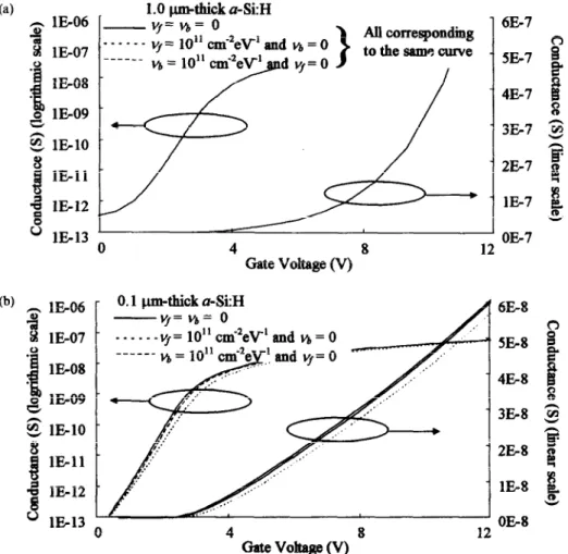
Finally, the effects of the states at the front inter- face and the rear interface are also investigated. For the thick semiconductor, the densities of the front interface states are much less than the total bulk state density and thus their effects cannot be observed. On the contrary, the front interface states for the thin active layer can degrade the electrical properties of the TFT’s as reported in a previous paper[9]. For the rear interface states, their effects are slightly apparent for the 0.1 pm-thick a-Si: H film, as shown in Fig. 7, and become more obvious for the TFT’s with ultra thin active layers.
The electrical field induced by the gate voltage can penetrate to the rear interface if the a-Si:H layer is thin enough. The states at the rear interface can help pinning the Fermi energy at the rear interface and thus, the potential distributions at different gate bias are not the same as those without rear interface 1.0
p-thick
u&H-vj=%$= 0
--- vf=l()“~-*eV’& ~a=0
>
All comesponding to the same curve dy,=O / 4 8 12 - 057 Gate Voltage (V) 0.1 p-thick a-Si:H -vf= I+#= 0 __..__ ~=1O”cm*eV’~d~=O I 0 4 8 12 0kG8 Gate voltage (V)
Fig. 7. The dependence of the field effect conductance on the gate voltage of the (a) 1.0 pm and (b) 0. I pm a-Si:H TFT’s with and without the interface states at the front and the rear interfaces.
0.01 I.utt-thick u&H
+ vf= Q.= O,QJ=@= 0
-u- v/= 10” cm”eV’, ti = 0, and QJ= Qb = 0 -G- y = 10” cr.ti2eV’, vf= 0, and a= Qb = 0 -e- (I&=10” cti2, Qb = 0, and v/= va = 0 & Qb =lO” cm”, a= 0, and v/= vs = 0
1 2 3 4 5 6 7 8
Gate Vohage (V)
Fig. 8. Effect of the interface states and fixed charges on the field effect conductance for the TFT’s with 0.01 pm-thick active layers.
states. Furthermore, the rear interface fixed charge can also generate an electrical field which will couple with that induced by the front gate voltage. The states, as well as the fixed charges at the rear inter- face, can modulate the band bending profiles if the active layer is thin. For the even thinner a-Q: H layer, their effects become much more important, as will be discussed in the next section.
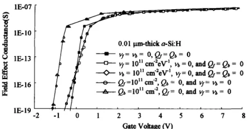
3.3. Ultra thin active layers
For the 0.01 pm-thick a-Si:H films, the curves of the field effect conductance vs the gate voltage of the TFT’s without and with the front or the rear interface state density of 10” cm-*eV-’ are calculated and plotted in Fig. 8. The states at the both interfaces considerably degrade the subthreshold behavior of the TFT’s. The rear interface states exhibit almost the same effect as the states at the front interface do. It reveals that if the active layer is very thin, the preparation of the rear interface is as important as that for the front interface.
The influences of the fixed charges density at the front and rear interfaces on the field effect conduc- tance of the TFT’s with 0.01 pm-thick active layers were also investigated. The fixed charges at the front and the rear interface show nearly the same effect. It depicts that for the TFT’s with very thin active layers, the characteristic of the rear interface can affect the performance of the TFT’s as much as the front interface does. Since the rear interface for the TFT’s is an interface of the a-Si:H and the passivation layer, it must be carefully treated while fabricating the passivation layer.
4. CONCLUSIONS
The band bending profiles of the semiconductor films with different thicknesses are calculated. It is found that if the thicknesses of the a-Si:H films are larger than the theoretical width of space charge region, which is about 5 pm, the potential distri- bution will behave like the infinitely thick films and
the rear interface exhibits little effect on the field effect conductance for the thick a-Si: H films. On the other hand, if the active layer thickness is less than this width, the zero-potential rear interface will be improper and the rigidly shifting behavior of the band bending will not be valid. Furthermore, for the 0.1 pm-thick or even thinner active layers, the properties of the rear interfaces can exhibit profound effects on the electrical characteristics of the TFT’s like those of the front interface. Therefore, it is necessary to consider the effects of both the film thickness and the rear front interface for the TFT’s with thin a-Si : H films.
Acknowledgements-The research was supported in part by the Republic of China National Science Council (ROC NSC) under the Contract no. NSC-84-2622-EOO9- 012. Technique supports from the Unipac Optoelectronics Corporation and the National Nano Device Laboratory of ROC NSC were also acknowledged.
I. 2. 3. 4. 5. 6. 7. 8. 9. 10. 11. 12. 13.
I. Magarino, Appl. Phys. A 41, 297 (1986).
N. B. Goodman, H. Fritzsche and H. Ozaki. J. Non- crystalline Solids 35 and 36, 599 (1980)
M. J. Powell, Phil. Mug. B 43, 9j (1981).
R. L. Weisfield and Anderson. Phil. Maz. B 44. 83 (1981).
T. Suzuki, Y. Osaka and M. Hirose, J. Appl. Phys. 21, Ll95 (1982).
M. Shur and M. Hack, J. Appl. Phys. 55, 3831 (1984). R. E. I. Schropp, J. Snijder and J. F. Verwey, J. Appl. Phys. 60, 643 (1986).
G. Fortunato and P. Migliorato, Appl. Phys. Lett. 49, 1025 (1986).
R. Saleh, N. Nickel, W. Fuhs and H. Mell, Marer. Res. Sot. Symp. Proc. 219, 339 (1991).
M. J. Powell and J. Pritchard, J. Appl. Phys. 54, 3244 (1983).
S. C. Deane, F. J. Clough, W. I. Milne and M. J. Powell, J. Appl. Phys. 73, 2895 (1993).
R. A. Smith, Hydrogenated Amorphous Silicon, Cambridge University Press, Cambridge (1991). J. G. Shaw and M. Hack, IEEE IEDM, San Francisco, CA, 13-16 December, pp. 915 (1992).
14. A. Rolland, J. Richard, J. P. Kleider and D. Mencaraglia, J. Electrochem. Sot. 140, 3679 (1993).